GENLINX ™ GS9007A Quad Serial Digital Cable Driver
DATA SHEET FEATURES • two output pairs (four outputs total) meeting SMPTE 259M • nominal 550 ps rise and fall times • accepts SMPTE and standard ECL input levels • operates from a single +5 or -5 volt supply • on-chip DC restoration for low jitter • 250mW power dissipation • Pb-free and Green APPLICATIONS • 4ƒSC, 4:2:2 and 360Mb/s Serial Digital Interfaces. The GENLINX ™ GS9007A is a bipolar intergrated circuit designed to drive four 75Ω co-axial cables with SMPTE level serial digital video signals at data rates up to 360Mb/s. It directly interfaces with other GENLINX ™ devices and can also be used as a general purpose high speed cable driver. The differential inputs are AC-coupled and internally DC-restored wich allows correct passage of pathological check codes associated with the serial digital standards. Even though the inputs are AC-coupled, static protection diodes at each input restrict the DC differential so that if the driving source uses the opposite polarity power supply, external DC blocking capacitors must be used. The GS9007A is packaged in an 8 pin SOIC, and operates from a single +5 or -5 volt supply consuming typically only 250mW of power.
GS9007A
NOT RECOMMENDED FOR NEW DESIGNS
ORDERING INFORMATION
PART NUMBER GS9007ACKA GS9007ACKAE3 PACKAGE TYPE 8 Pin SOIC 8 Pin SOIC TEMPERATURE RANGE 0°C to 70°C 0°C to 70°C Pb-FREE AND GREEN No Yes
8
VCC (GND) SDO1
GS9007A
1
2 SERIAL INPUT SERIAL INPUT 7 INPUT BUFFER & DC 6 RESTORE RISE TIME CONTROL
SDO1
3
SDO2
4
SDO2
5
GND (VEE)
FUNCTIONAL BLOCK DIAGRAM
Revision Date: June 2005 GENNUM CORPORATION P.O. Box 489, Stn. A, Burlington, Ontario, Canada L7R 3Y3 Tel. +1 (905) 632-2996 Fax. +1 (905) 632-5946 E-mail: info@gennum.com www.gennum.com
Document No. 24009 - 2
�PIN CONNECTIONS
TOP VIEW 1
SERIAL OUT -1 SERIAL OUT -1 SERIAL OUT -2 SERIAL OUT -2
VCC (GROUND) SERIAL INPUT
GS9007A
SERIAL INPUT GROUND (VEE)
DC ELECTRICAL CHARACTERISTICS
VS = 5V, TA = 0°C to 70°C, RL = 150Ω to GND and 143Ω AC coupled unless otherwise shown.
NOT RECOMMENDED FOR NEW DESIGNS
PARAMETER Supply Voltage Power Consumption Supply Current
SYMBOL VS PD IS1 IS2
CONDITIONS Operating Range 4x15W Loads DC 1% Accurancy, TA = 25°C DC No Loads, TA = 25°C
MIN 4.5 -
TYP 5.0 250
MAX 5.5 290
UNITS V mW
NOTES
-
105 17.2
110 22
mA mA
AC ELECTRICAL CHARACTERITICS
VS = 5V, TA = 0°C to 70°C, RL = 150Ω to GND and 143Ω AC coupled unless otherwise shown.
PARAMETER SERIAL DIGITAL SIGNALS Signal Swing Rise/Fall Times
SYMBOL VIN tR, tF tR, tF
CONDITIONS
MIN 700 -
TYP 800 -
MAX 1000 750
UNITS mVp-p ps
NOTES
measured at 20% and 80% measured at 20% and 80%
Rise/Fall Times SERIAL DIGITAL OUTPUTS
400
550
800
ps
Jitter Propagation Delay Output Overshoot Signal Swing
tJ tP
at 270Mb/s
-
1 0 800
±25 880
ps ns % mVp-p see Figure 4
tR = tJ = 600 ps VOUT Across 75Ω Load
720
2 of 4
GENNUM CORPORATION
24009 - 2
�ABSOLUTE MAXIMUM RATINGS
PARAMETER Supply Voltage (VS) Input Voltage Range (any input) Power Dissipation Operating Tempature Range Storage Temperature Range Lead Tempature (Soldering, 10.sec) VALUES/UNITS 5.5V VS -0.5V 300mW 0°C < TA < 70°C -65°C < TS < 150°C 260°C
VCC
VCC 400 400
GS9007A
SDO
VCC
NOT RECOMMENDED FOR NEW DESIGNS
INPUT / OUTPUT CIRCUITS
VCC
SDO
VCC
Fig. 2 Output Circuit (Pins 1, 2 and 3, 4)
SERIAL INPUTS VREF1 0.5p 400 VREF1 + VREF2
-5V
+5V
7 ECL DRIVER 0.1µF GS9007A 6 0.1µF
Fig. 1 Input Circuit (Pins 6 and 7)
-2V
Fig. 3 Split Supply Interfacing
3 of 4
GENNUM CORPORATION
24009 - 2
�+5V + 10 8 1 68 1.0 1p8 7 68 1.0 1p8 3 4 5 150 150 1.0
All resistors in ohms, all capacitors in microfarards unless otherwise stated.
0.1 75 COAX
GS9007A
2 75 75 COAX
GS9007A
SERIAL DIGITAL INPUTS
150 6
150
75 68 75 COAX
1.0 1p8 68 75 COAX
75
NOT RECOMMENDED FOR NEW DESIGNS
75 1p8
Fig. 4 Typical Application Circuit
CAUTION
ELECTROSTATIC SENSITIVE DEVICES
DO NOT OPEN PACKAGES OR HANDLE EXCEPT AT A STATIC-FREE WORKSTATION
DOCUMENT IDENTIFICATION
DATA SHEET The product is in production. Gennum reserves the right to make changes at any time to improve reliability, function or design, in order to provide the best product possible.
REVISION NOTES: Version 1 - Adding lead-free and green information. Version 2 - Adding minimum Rise / Fall time.
GENNUM CORPORATION
MAILING ADDRESS: P.O. Box 489, Stn. A, Burlington, Ontario, Canada L7R 3Y3 Tel. +1 (905) 632-2996 Fax. +1 (905) 632-5946 SHIPPING ADDRESS: 970 Fraser Drive, Burlington, Ontario, Canada L7L 5P5
GENNUM JAPAN CORPORATION Shinjuku Green Tower Building 27F 6-14-1, Nishi Shinjuku Shinjuku-ku, Tokyo 160-0023 Japan Tel: +81 (03) 3349-5501 Fax: +81 (03) 3349-5505 GENNUM UK LIMITED 25 Long Garden Walk, Farnham, Surrey, England GU9 7HX Tel. +44 (0)1252 747 000 Fax +44 (0)1252 726 523
Gennum Corporation assumes no responsibility for the use of any circuits described herein and makes no representations that they are free from patent infringement. © Copyright May 2002 Gennum Corporation. All rights reserved. Printed in Canada.
4 of 4
24009 - 2
�
很抱歉,暂时无法提供与“GS9007ACKA”相匹配的价格&库存,您可以联系我们找货
免费人工找货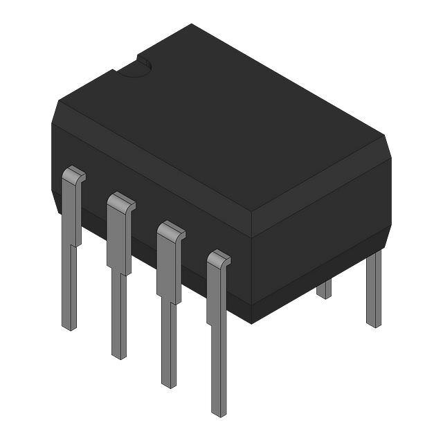


 工商网监
湘ICP备2023018690号
工商网监
湘ICP备2023018690号
