LR1121
Long range, Low Power, Multi-band
LoRa® Transceiver
PA
HF
LoRa
modem
(G)FSK
modem
LNA
HF
ADC
LNA
LF0
PA
LP LF
PLL
Digital Baseband
+ DSP
Digital Front-End
NVM
CPU
PA
HP LF
ROM
REGs
RAM
CKS
PDS
REG_PA
IO Control
Balun
&
Match
DC-DC
LDO
BG/IREF
POR/
BRN
The LR1121 is an ultra-low power, long range LoRa®
transceiver that provides support for terrestrial ISM band
communications in the sub-GHz and global 2.4GHz
spectrum, as well as S-Band support for satellite
connectivity.
HFRC
32MHz
HFXOSC
32MHz
LFXOSC
32kHz
LFRC
32kHz
The transceiver is suitable for systems targeting
compliance with radio standards including but not limited
to ETSI EN 300 220, FCC CFR 47 Part 15, ARIB, and Chinese
regulatory requirements.
For all varieties of LPWAN use case, the LR1121 supports
any combination of LoRa, (G)FSK, Long Range FHSS
(LR-FHSS) modulations.
The LR1121 complies with the physical layer requirements
of the LoRa Alliance® LoRaWAN® specification, while
remaining configurable to meet different application
requirements and proprietary protocols.
LR1121
Datasheet
DS.LR1121.W.APP
Rev 1.1
Mar 2023
www.semtech.com
1 of 35
Semtech
Proprietary & Confidential
�Disclaimer
Long Range-Frequency Hopping Spread Spectrum (LR-FHSS) is a high link-budget, high-performance
technology combining the benefits of a modulation employing low energy per bit and advanced frequency
hopping schemes to achieve improved coexistence, spectral efficiency and sensitivity. Semtech Corp. holds
patents directed to aspects of the LR-FHSS technology.
Your use of LR-FHSS software made available by Semtech Corp. or its affiliates does not grant any rights to
their patents for LR-FHSS technology. Rights under Semtech patents may be available via various
mechanisms, including by purchasing Semtech SX1261, SX1262, SX1268, LR1110, LR1120, or LR1121
semiconductor devices, or their authorized counterparts from Semtech, or its affiliates, or their respective
licensees.
Ordering Information
Part Number
Delivery
LR1121IMLTRT
Tape & Reel
Minimum Order Quantity
3000 pieces
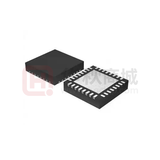
QFN32 Package, Pb-free, Halogen free, RoHS/WEEE compliant product.
Revision History
Version
ECO
Date
1.0
062817
Jul 2022
Applicable to1
Use Case: 03
FW version: 01.00 or later
Changes
First Release
Include S-Band information
Modified BRLORA RFIO_HF 2.4GHz typical value
Section 1.2.4 rewritten
Add reference to AN1200.74 in section 4.5
1.1
065940
Mar 2023
Use Case: 03
FW version: 01.00 or later
Modified section 1.2.1: air interface
Modified Pinout pin 26 description
Modified first 3 bullets of section 3.4
Added IDDTXHF3 & IDDTXHF4, & RXSLHF7 &
RXSLHF10 parameters
Modified section 4.1
Added section 5.6 Tape and Reel Information
1. Use Case and Version concepts are defined in the LR1121 User Manual, see the GetVersion command.
LR1121
Datasheet
DS.LR1121.W.APP
Rev 1.1
Mar 2023
www.semtech.com
2 of 35
Semtech
Proprietary & Confidential
�Table of Contents
1. System Description .........................................................................................................................................6
1.1 Simplified Block Diagram ................................................................................................................6
1.2 Overview ................................................................................................................................................7
1.2.1 Low-Power High-Sensitivity LoRa®/(G)FSK Half-Duplex RF Transceiver ............7
1.2.2 Multi-Purpose Radio Front-End.........................................................................................7
1.2.3 Power Management..............................................................................................................7
1.2.4 Clock Sources...........................................................................................................................7
1.2.5 Digital Subsystem ..................................................................................................................8
1.2.6 Cryptographic Engine...........................................................................................................8
2. Pin Connection .................................................................................................................................................9
3. Specifications ................................................................................................................................................. 11
3.1 Absolute Maximum Ratings ........................................................................................................ 11
3.2 Operating Range .............................................................................................................................. 11
3.3 ESD and Latch-up ............................................................................................................................ 12
3.4 Electrical Specifications ................................................................................................................. 12
3.4.1 Power Consumption .......................................................................................................... 12
3.4.2 General Specifications ...................................................................................................... 15
3.4.3 Receiver .................................................................................................................................. 16
3.4.4 Transmitter ............................................................................................................................ 20
3.5 Reference Oscillator ........................................................................................................................ 21
3.6 Digital I/O, Flash Memory, & Interface Specifications ........................................................ 22
3.6.1 Digital I/O Specifications .................................................................................................. 22
3.6.2 Flash Memory Specifications........................................................................................... 22
3.6.3 SPI Interface........................................................................................................................... 22
4. Application Information............................................................................................................................. 23
4.1 LR-FHSS Modulation ....................................................................................................................... 23
4.2 Exiting Sleep Mode ......................................................................................................................... 23
4.3 Digital Inputs/Outputs ................................................................................................................... 24
4.3.1 DIO Configuration............................................................................................................... 24
4.3.2 RF Switch Control ................................................................................................................ 24
4.3.3 Reset......................................................................................................................................... 24
4.3.4 Host Interrupts ..................................................................................................................... 25
4.4 Firmware Upgrade/ Update ......................................................................................................... 25
4.5 Simplified Reference Schematic ................................................................................................ 26
4.6 Example Reference Layout ........................................................................................................... 27
5. Package Information ................................................................................................................................... 28
5.1 Package Outline Drawing ............................................................................................................. 28
5.2 Package Marking ............................................................................................................................. 29
5.3 Land Pattern ...................................................................................................................................... 30
5.4 Reflow Profiles .................................................................................................................................. 30
5.5 Thermal Information ...................................................................................................................... 31
5.6 Tape & Reel Information ............................................................................................................... 31
LR1121
Datasheet
DS.LR1121.W.APP
Rev 1.1
Mar 2023
www.semtech.com
3 of 35
Semtech
Proprietary & Confidential
�List of Figures
Figure 1-1: LR1121 Simplified Block Diagram ........................................................................................ 6
Figure 2-1: LR1121 Pinout ............................................................................................................................. 10
Figure 4-1: Multi-band EU/US LoRaWAN Using Sub-GHz PAs ....................................................... 26
Figure 4-2: Reference Design Layout ....................................................................................................... 27
Figure 5-1: Package Outline Drawing ....................................................................................................... 28
Figure 5-2: Package Marking ....................................................................................................................... 29
Figure 5-3: Land Pattern ................................................................................................................................ 30
Figure 5-4: Tape & Reel Information.......................................................................................................... 31
LR1121
Datasheet
DS.LR1121.W.APP
Rev 1.1
Mar 2023
www.semtech.com
4 of 35
Semtech
Proprietary & Confidential
�List of Tables
Table 2-1: LR1121 Pinout.................................................................................................................................. 9
Table 3-1: Absolute Maximum Ratings.................................................................................................... 11
Table 3-2: Operating Range......................................................................................................................... 11
Table 3-3: ESD and Latch-up ....................................................................................................................... 12
Table 3-4: Basic Modes Power Consumption......................................................................................... 12
Table 3-5: Receive Mode Power Consumption, DC-DC mode used .............................................. 13
Table 3-6: Transmit Mode Power Consumption ................................................................................... 14
Table 3-7: General Specifications ............................................................................................................... 15
Table 3-8: Receiver Specifications, Sub-GHz Bands ............................................................................. 16
Table 3-9: Receiver Specifications, S-band and 2.4GHz ISM band.................................................. 18
Table 3-10: Transmitter Specifications, sub-GHz Path........................................................................ 20
Table 3-11: Transmitter Specifications, S-band and 2.4GHz ISM band......................................... 20
Table 3-12: 32MHz Crystal Specifications............................................................................................... 21
Table 3-13: 32MHz TCXO Regulator Specifications ............................................................................ 21
Table 3-14: 32kHz Crystal Specifications ................................................................................................ 21
Table 3-15: Digital I/O and NRESET Specifications ............................................................................... 22
Table 3-16: Flash Memory Specifications ................................................................................................ 22
Table 3-17: SPI Timing Requirements ....................................................................................................... 22
Table 4-1: LR1121 DIO Mapping ................................................................................................................. 24
Table 5-1: Package Thermal Information................................................................................................. 31
LR1121
Datasheet
DS.LR1121.W.APP
Rev 1.1
Mar 2023
www.semtech.com
5 of 35
Semtech
Proprietary & Confidential
�1. System Description
1.1 Simplified Block Diagram
1.9 - 2.6GHz, RX/TX
Figure 1-1: LR1121 Simplified Block Diagram
RFIO_HF
Balun
&
Match
PA
HF
LoRa
modem
(G)FSK
modem
LNA
HF
DIO0/ BUSY
DIO1
ADC
NVM
DIO2
PA
LP LF
RFO_LP_LF
PLL
CPU
DIO4
DIO5
DIO6
DIO7
DIO8
PA
HP LF
RFO_HP_LF
IO Control
RFI_P_LF0
LNA
LF0
Digital Baseband
+ DSP
RFI_N_LF0
Digital Front-End
150 - 960MHz, RX/TX
DIO3
ROM
RAM
DIO9
nRESET
LR1121
Datasheet
DS.LR1121.W.APP
Rev 1.1
Mar 2023
www.semtech.com
LFXOSC
32kHz
DIO11/ 32k_P
LFRC
32kHz
DIO10/32k_N
HFXOSC
32MHz
XTB
HFRC
32MHz
XTA
VBAT_RF
DCC_SW
VBAT_DCC
REGs
VREG
REG_PA
BG/IREF
POR/
BRN
DC-DC
LDO
VTCXO
VR_PA
CKS
PDS
VBAT_RF
6 of 35
Semtech
Proprietary & Confidential
�1.2 Overview
1.2.1 Low-Power High-Sensitivity LoRa®/(G)FSK Half-Duplex RF Transceiver
•
Worldwide frequency bands support in the range 150 - 960MHz (sub-GHz),1.9-2.1GHz S-band and 2.4GHz ISM band.
•
Low Noise Figure modes for enhanced LoRa/ (G) FSK sensitivity (differential input pins RFI_P/N_LF0)
•
High power PA path +22dBm (pin RFO_HP_LF) and High efficiency PA path +15dBm (pin RFO_LP_LF) for sub-GHz
•
High frequency PA path +13dBm (pin RFIO_HF) for 2.4GHz ISM band and S-band, matched to 50Ohm impedance,
reducing the overall Bill Of Materials cost
•
Integrated PA regulator supply selector to simplify dual power +15/+22dBm with a single board implementation
•
Able to support world-wide multi-region BOM, the circuit adapts to satisfy regulatory limits
•
Air interface fully compatible with the SX1261/2/8 family and the LoRaWAN standard, defined by the LoRa Alliance
•
LR-FHSS Transmitter, with intra-packet hopping capability
1.2.2 Multi-Purpose Radio Front-End
•
Continuous frequency synthesizer range from 150MHz - 2.5GHz
1.9 to 2.5GHz handled by the RFIO_HF RF port, already matched to 50 Ohms
All sub-GHz support handled by the other RF ports
•
Digital baseband
1.2.3 Power Management
•
Two forms of voltage regulation (DC-DC or linear regulator, LDO) are available depending upon the design priorities of
the application. DC-DC usage is recommended for power efficient operation at the cost of an extra inductor.
•
Power On Reset (POR), Brown-out detection and Low Battery indication are supported
•
Battery voltage measurement
1.2.4 Clock Sources
•
32.768kHz Low Frequency (LF) internal RC oscillator, optionally used by the circuit Real Time Clock (RTC)
•
32.768kHz LF crystal oscillator (XOSC), used for the RTC. An external 32.768kHz reference from a host, applied to pin
DIO11, is also possible.
•
32MHz HF RC (HFRC) oscillator allows configuration of the device without the need to start the main crystal oscillator
•
32MHz HF crystal oscillator (HFXOSC) for radio operations and to calibrate frequency error of internal RC oscillators
•
32MHz TCXO can be used to supply the main clock to the circuit, its power supply being integrated on-chip by
REG_TCXO, on pin VTCXO. The circuit is able to boot when a TCXO is connected instead of a 32MHz crystal, however all
start-up (POR) calibrations are skipped. The host processor should program the TCXO configuration and re-launch the
calibrations before further usage of the chip.
•
For additional guidance on external clock sources (crystal and TCXO), refer to Section 4.5.
LR1121
Datasheet
DS.LR1121.W.APP
Rev 1.1
Mar 2023
www.semtech.com
7 of 35
Semtech
Proprietary & Confidential
�1.2.5 Digital Subsystem
The circuit on-boards power-efficient functionalities, with sufficient hardware resources to implement a wide range of
applications:
•
Logic to control chip modes, radio front-end, power management and digital interfaces
•
RAM partially retained during sleep mode
•
Non-volatile memory (NVM)
•
Slave serial peripheral interface (SPI)
•
DIO0 used as “BUSY” indicator, indicating that the internal MCU cannot receive any commands from the host
controller
•
Hardware de-bounce and event detection (IOCD)
•
Low-power real-time counter (RTC) and watch-dog timer (WDG)
•
LoRa, (G)FSK, modems compatible with the SX126x and SX127x product families in sub-GHz bands
•
LoRa, (G)FSK, modems compatible with the SX128x product families in the 2.4GHz ISM band
•
Long Range FHSS in transmit mode, with intra-packet hopping capability
1.2.6 Cryptographic Engine
•
Hardware support for AES-128 encryption/decryption based algorithms
•
Handling device parameters such as DevEUI and JoinEUI, as defined by the LoRa Alliance
•
Protects confidential information such as encryption keys against unauthorized access
•
Stores NwkKey, AppKey, as defined in the LoRaWAN standard
LR1121
Datasheet
DS.LR1121.W.APP
Rev 1.1
Mar 2023
www.semtech.com
8 of 35
Semtech
Proprietary & Confidential
�2. Pin Connection
Table 2-1: LR1121 Pinout
Pin
Name
Type
0
GND
-
Exposed Ground pad
1
VR_PA
O
Regulated power amplifier supply, for all power amplifiers
2
VBAT_RF
I
Battery supply
3
VTCXO
O
Internally generated supply for external TCXO frequency reference
4
XTA
-
32MHz crystal connection, or external TCXO frequency reference input
5
XTB
-
32MHz crystal connection, or NC in case of external TCXO usage
6
NRESET
I
Reset signal, active low
7
32k_P/ DIO11
I/O
32.768kHz crystal connection, or input for 32.768kHz reference clock/ Multi-purpose
digital I/O
8
32k_N/ DIO10
I/O
32.768kHz crystal oscillator connection/ Multi-purpose digital I/O
9
DIO9
I/O
Multi-purpose digital I/O
10
DIO8
I/O
Multi-purpose digital I/O
11
DIO7
I/O
Multi-purpose digital I/O
12
VREG
O
Regulated output voltage from the internal regulator LDO/ DC-DC
13
GND
-
Ground
14
DCC_SW
-
DC-DC Switcher Output
15
VBAT
I
Battery supply
16
DNC
-
Do not connect
17
DNC
-
Do not connect
18
DNC
-
Do not connect
19
DIO6
I/O
Multi-purpose digital I/O
20
DIO5
I/O
Multi-purpose digital I/O
21
DIO4
I/O
Multi-purpose digital I/O
22
DIO3
I/O
Multi-purpose digital I/O
23
DIO2
I/O
Multi-purpose digital I/O
24
DIO1
I/O
Multi-purpose digital I/O
25
DIO0/BUSY
I/O
Multi-purpose digital I/O
26
RFIO_HF
I/O
RF input/output for any frequency over 1.9GHz
27
DNC
-
Do not connect
28
DNC
-
Do not connect
29
RFI_N_LF0
I
RF LF receiver input, sub-GHz operation
30
RFI_P_LF0
I
RF LF receiver input, sub-GHz operation
31
RFO_LP_LF
O
RF transmitter output for the low power PA, sub-GHz operation
32
RFO_HP_LF
O
RF transmitter output for the high power PA, sub-GHz operation
LR1121
Datasheet
DS.LR1121.W.APP
Rev 1.1
Mar 2023
Description
www.semtech.com
9 of 35
Semtech
Proprietary & Confidential
�RFO_HP_LF
RFO_LP_LF
RFI_P_LF0
RFI_N_LF0
DNC
DNC
RFIO_HF
DIO0/BUSY
Figure 2-1: LR1121 Pinout
32
31
30
29
28
27
26
25
VR_PA
1
24
DIO1
VBAT_RF
2
23
DIO2
VTCXO
3
22
DIO3
XTA
4
21
DIO4
XTB
5
20
DIO5
NRESET
6
19
DIO6
32k_P/
DIO11
7
18
DNC
32k_N/
DIO10
8
17
DNC
LR1121
Datasheet
DS.LR1121.W.APP
Rev 1.1
Mar 2023
14
15
16
DNC
DIO7
13
VBAT
DIO8
12
DCC_SW
11
GND
10
VREG
9
DIO9
0
www.semtech.com
10 of 35
Semtech
Proprietary & Confidential
�3. Specifications
3.1 Absolute Maximum Ratings
Stresses above the values listed below may cause permanent device failure. Exposure to absolute maximum ratings for
extended periods may affect device reliability, reducing product life time.
Table 3-1: Absolute Maximum Ratings
Symbol
Description
Min
Typ
Max
Unit
VDDmr
Supply voltage
-0.5
-
3.9
V
Tmr
Temperature
-55
-
125
°C
Pmr
RF Input level
-
-
10
dBm
3.2 Operating Range
Operating ranges define the limits for functional operation and parametric characteristics of the device as described in this
section. Functionality outside these limits is not guaranteed.
Table 3-2: Operating Range
Symbol
Description
VDDop
Min
Typ
Max
Unit
Supply voltage
1.8
-
3.7
V
Top
Temperature under bias (ambient)
-40
-
85
°C
Clop
Load capacitance on digital ports
-
-
20
pF
ML
Maximum Input power
Sub-GHz path
-
-
0
dBm
VSWR
Voltage Standing Wave Ratio
Sub-GHz and RFIO_HF path
-
-
10:1
-
LR1121
Datasheet
DS.LR1121.W.APP
Rev 1.1
Mar 2023
Conditions
www.semtech.com
11 of 35
Semtech
Proprietary & Confidential
�3.3 ESD and Latch-up
The LR1121 is a high performance radio frequency device presenting high ESD and latch-up robustness on all pins. The chip
should be handled with all the necessary ESD precautions to avoid any permanent damage.
Table 3-3: ESD and Latch-up
Symbol
Description
Min
Typ
Max
Unit
ESD_HBM
Human Body Model, JEDEC standard JESD22-A114, class II
-
-
2.0
kV
ESD_CDM
ESD Charged Device Model, JEDEC standard JESD22-C101, class II
-
-
500
V
LU
Latch-up, JEDEC standard JESD78, class II level A
-
-
100
mA
3.4 Electrical Specifications
The tables below give the electrical specifications of the LR1121 transceiver under the following conditions, unless
otherwise specified:
•
VBAT_RF = VBAT = 3.3V, Temperature = 25°C, FXOSC = 32MHz, crystal oscillator
•
FRF = 915/869MHz on sub-GHz path RFI_N/P_LF0 and RFO_HP/LP_LF for FSK and LoRa
•
Satellite band (S-band) in these tables describes specifications between 1.9 and 2.2GHz
•
FRF = S-band and 2.45GHz for the RFIO_HF path, same BOM used for all S-band and 2.45GHz specifications
•
All RF impedances on the sub-GHz and RFIO_HF path are matched using multi-band reference design, transmit mode
output power defined in 50load, RxBoosted = 1 for LoRa and FSK, differential use of the LNAs (receiver gain levels
are referenced in the device’s User Manual)
•
FSK Bit Error Rate (BER) = 0.1%, 2-level FSK modulation without pre-filtering, BR = 4.8kb/s, FDA = 5kHz, BWF = 20kHz,
•
LoRa Packet Error Rate (PER) = 1%, BWL= 125kHz, packet of 64 bytes, preamble of 8 symbols, error correction code
CR=4/5, CRC on payload enabled, explicit header, sub-GHz frequency range
•
Blocking Immunity, ACR, and co-channel rejection are given for a single tone interferer and referenced to sensitivity
+3dB, blocking tests are performed with unmodulated interferer
•
All power consumption numbers are given with XTAL mode used, the consumption of the TCXO has to be added
•
All receiver bandwidths (BW) are expressed as Double SideBand (DSB) throughout this document
3.4.1 Power Consumption
The tables below give the total consumptions of all blocks in the specified modes of the circuit.
Table 3-4: Basic Modes Power Consumption
Symbol
Description
IDDPDN
Supply current in power down mode
IDDSL3
Supply current in SLEEP mode, no RTC
IDDSL1
IDDSL3A
LR1121
Datasheet
DS.LR1121.W.APP
Min
Typ
Max
Unit
-
0.8
-
A
8kB RAM retained
-
1.6
-
A
Supply current in SLEEP mode
No RAM retained
-
1.6
-
A
LFRC (32kHz) based RTC
8kB RAM retained
-
1.85
-
A
Rev 1.1
Mar 2023
Conditions
www.semtech.com
12 of 35
Semtech
Proprietary & Confidential
�Table 3-4: Basic Modes Power Consumption
Symbol
Description
Conditions
Min
Typ
Max
Unit
IDDSL2
Supply current in SLEEP mode
No RAM retained
-
1.5
-
A
IDDSL4A
LFXOSC (32kHz) based RTC
8kB RAM retained
-
1.75
-
A
IDDSBRLD
Supply current in STBY_RC
-
1.25
-
mA
IDDSBXLD
Supply current in STBY_XOSC
IDDSBXDC
IDDFSDC
Supply current in Synthesizer mode
HFRC (32MHz) ON, LDO,
System clock 16MHz
HFXOSC ON, LDO
-
1.3
-
mA
HFXOSC ON, DC-DC
-
1.1
-
mA
DC-DC, system clock 32MHz
-
2.85
-
mA
Table 3-5: Receive Mode Power Consumption, DC-DC mode used
Symbol
Description
IDDRXF1
IDDRXF2
IDDRXL1
Supply current in Receive mode
IDDRXL2
LR1121
Datasheet
DS.LR1121.W.APP
Rev 1.1
Mar 2023
Conditions
Min
Typ
Max
Unit
FSK 4.8kb/s sub-GHz
-
5.4
-
mA
with RxBoosted = 1
-
7.5
-
mA
FSK 4.8kb/s 2.4GHz/S-band
-
5.9
-
mA
with RxBoosted = 1
-
6.6
-
mA
LoRa® SF12 125kHz sub-GHz
-
5.7
-
mA
with RxBoosted = 1
-
7.8
-
mA
LoRa® SF12 125kHz 2.4GHz/S-band
-
6
-
mA
with RxBoosted = 1
-
6.7
-
mA
LoRa® SF12 406kHz 2.4GHz/S-band
-
7.6
-
mA
with RxBoosted = 1
-
8.3
-
mA
LoRa® SF12 812kHz 2.4GHz/S-band
-
6.8
-
mA
with RxBoosted = 1
-
7.5
-
mA
www.semtech.com
13 of 35
Semtech
Proprietary & Confidential
�Table 3-6: Transmit Mode Power Consumption1
Symbol
Frequency Band
PA Match
Output Power
Min
Typ
Max
Unit
+15dBm
-
36
-
mA
+14dBm
-
28
-
mA
+10dBm
-
18.5
-
mA
+15dBm
-
35
-
mA
+14dBm
-
28
-
mA
IDDTXLP6
+10dBm
-
19
-
mA
IDDTXHP1
+22dBm
-
118
-
mA
+20dBm
-
96
-
mA
+17dBm
-
73
-
mA
+14dBm
-
50
-
mA
+22dBm
-
100
-
mA
+20dBm
-
86
-
mA
+17dBm
-
70
-
mA
+14dBm
-
45
-
mA
+13dBm
-
26
-
mA
+10dBm
-
23
-
mA
+13dBm
-
28
-
mA
+10dBm
-
24
-
mA
IDDTXLP1
IDDTXLP2
868/915MHz
IDDTXLP3
+14dBm, LP PA2
IDDTXLP4
IDDTXLP5
IDDTXHP2
IDDTXHP3
434/490MHz
868/915MHz
IDDTXHP4
+22dBm, HP PA3
IDDTXHP5
IDDTXHP6
IDDTXHP7
434/490MHz
IDDTXHP8
IDDTXHF1
IDDTXHF2
IDDTXHF3
IDDTXHF4
2.4GHz
+13dBm, HF PA
S-band
+13dBm, HF PA
1. Using optimized settings described in the LR1121 User Manual
2. DC-DC mode of the LDO/DC-DC combo is used to supply the entire circuit
3. Battery used to supply the PA, and DC-DC used to supply the rest of the circuit
LR1121
Datasheet
DS.LR1121.W.APP
Rev 1.1
Mar 2023
www.semtech.com
14 of 35
Semtech
Proprietary & Confidential
�3.4.2 General Specifications
Table 3-7: General Specifications
Symbol
Description
FRSYNTH
Synthesizer frequency range
FSTEP
Synthesizer frequency step
HFOSCCP
32MHz Crystal oscillator supported
off-chip capacitance
OSCTRM1
Min
Typ
Max
Unit
150
-
2500
MHz
FXOSC/ 225
-
0.9536
-
Hz
Single ended on XTA and XTB
0.2
1
3
pF
HF Crystal oscillator trimming step
-
1
-
ppm
LFCLKFR
Frequency of external LF clock applied
on pin DIO11
-
32.768
-
kHz
LFCLKRF
Rise/fall time for external LF clock
applied on pin DIO11
-
-
5
ns
Bit rate, FSK
Programmable, lowest setting
-
0.6
-
kb/s
Minimum modulation index is 0.5
Programmable, highest setting
-
3001
-
kb/s
Programmable
FDA + BRF / 2 250kHz
-
0.6
200
-
kHz
kHz
Raw data rate, LoRa, sub-GHz
SF12, BWL = 62.5kHz, CR = 1/2
SF5, BWL = 500kHz, CR = 4/5
-
91
62.5
-
b/s
kb/s
Raw data rate, LoRa, RFIO_HF S-band
SF12, BWL=125kHz, CR=4/5
SF5, BWL=500kHz, CR=4/5
-
0.292
87.5
-
-
-
kb/s
kb/s
Raw data rate, LoRa, RFIO_HF 2.4GHz
SF12, BWL=203kHz, CR=4/5
SF5, BWL=812kHz, CR=4/5
-
0.476
101.5
-
kb/s
kb/s
Signal BW, LoRa
Programmable, lowest setting
Programmable, highest setting
-
62.5
5002
-
kHz
kHz
Signal BW, LoRa, RFIO_HF S-band
Programmable, lowest setting
Programmable, highest setting
-
125
-
kHz
kHz
Signal BW, LoRa, RFIO_HF 2.4GHz
Programmable, lowest setting
Programmable, highest setting
-
500
-
-
203
812
-
kHz
kHz
Spreading factor coefficient, LoRa
Programmable, lowest setting
-
5
-
-
chips/symbol = 2^SF
Programmable, highest setting
-
12
-
-
DSB channel filter BW, FSK,
Programmable, lowest setting
-
4.8
-
kHz
sub-GHz path
Programmable, highest setting
-
467
-
kHz
BRFSK
FDAFSK
BRLORA
Conditions
Frequency deviation, FSK
BWL
SF
BWF
1. Maximum bit rate is assumed to scale with the RF frequency; example 300kb/s in the 869/915MHz frequency bands and only 50kb/s @150MHz
2. For RF frequencies below 300MHz, the LoRa signal BW is limited to maximum 250kHz, the data rate being reduced accordingly
LR1121
Datasheet
DS.LR1121.W.APP
Rev 1.1
Mar 2023
www.semtech.com
15 of 35
Semtech
Proprietary & Confidential
�3.4.3 Receiver
Table 3-8: Receiver Specifications, Sub-GHz Bands
Symbol
Description
Conditions
Min
Typ
Max
Unit
FRRXLF
RX input frequency
Sub-GHz frequency range, LoRa and FSK1
150
-
960
MHz
Impedance across RFI_N_LF0 / RFI_P_LF02
433MHz
-
29 - j289
-
Ohm
868MHz
-
9.4 - j141
-
Ohm
920MHz
-
9.5 - j131
-
Ohm
100kHz offset
-
-102
-
dBc/Hz
1MHz offset
-
-120
-
dBc/Hz
10MHz offset
-
-129
-
dBc/Hz
RXS2F1
BRF = 0.6kb/s, FDA = 0.8kHz, BWF = 4kHz
-
-123
-
dBm
RXS2F2
BRF = 1.2kb/s, FDA = 5kHz, BWF = 20kHz
-
-122
-
dBm
ZINRXLF
RX input impedance
PHNLF1
Synthesizer phase
noise3,4 sub-GHz band
PHNLF2
PHNLF3
RXS2F3
Sensitivity 2-FSK
BRF = 4.8kb/s, FDA = 5kHz, BWF = 20kHz
-
-117.5
-
dBm
RXS2F4
BRF = 38.4kb/s, FDA = 40kHz, BWF = 160kHz
-
-109
-
dBm
RXS2F5
BRF = 250kb/s, FDA = 125kHz, BWF = 500kHz
-
-103.5
-
dBm
RXS2F1HP3
BRF = 0.6kb/s, FDA = 0.8kHz, BWF = 4kHz
-
-125
-
dBm
BRF = 1.2kb/s, FDA = 5kHz, BWF = 20kHz
-
-124
-
dBm
BRF = 4.8kb/s, FDA = 5kHz, BWF = 20kHz
-
-119
-
dBm
BRF = 38.4kb/s, FDA = 40kHz, BWF = 160kHz
-
-111
-
dBm
BRF = 250kb/s, FDA = 125kHz, BWF = 500kHz
-
-105
-
dBm
-
-8
-
dB
-
47
-
dB
Offset = +/- 1MHz
-
67
-
dB
Offset = +/- 2MHz
-
70
-
dB
Offset = +/- 10MHz
-
80
-
dB
Unwanted tones @1MHz and 1.96MHz
-
-12
-
dBm
Without IQ calibration
-
40
-
dB
With IQ calibration
-
50
-
dB
RXSL1
BWL = 62.5kHz, SF = 7
-
-128
-
dBm
RXSL2
BWL = 62.5kHz, SF = 12
-
-142
-
dBm
RXSL3
BWL = 125kHz, SF = 7
-
-125
-
dBm
BWL = 125kHz, SF = 12
-
-139
-
dBm
BWL = 250kHz, SF = 7
-
-122
-
dBm
RXSL6
BWL = 250kHz, SF = 12
-
-136
-
dBm
RXSL7
BWL = 500kHz, SF = 7
-
-118
-
dBm
RXSL8
BWL = 500kHz, SF = 12
-
-132
-
dBm
RXS2F2HP3
Sensitivity 2-FSK,
RXS2F3HP3
RxBoosted = 1
RXS2F4HP3
RXS2F5HP3
CCRFSK
Co-channel rejection, FSK
ACRFSK
Adjacent channel
rejection, FSK
Offset = +/- 50kHz
BRF = 4.8 kb/s, FDA = 5kHz, BWF = 20kHz
BIFSK1
BIFSK2
Blocking immunity, FSK
BIFSK3
IIP3FSK
3rd order input intercept
point, FSK
IMRFSK
Image attenuation,
sub-GHz path
RXSL4
RXSL5
LR1121
Datasheet
DS.LR1121.W.APP
Sensitivity LoRa
Rev 1.1
Mar 2023
www.semtech.com
16 of 35
Semtech
Proprietary & Confidential
�Table 3-8: Receiver Specifications, Sub-GHz Bands (Continued)
Symbol
Description
Conditions
Min
Typ
Max
Unit
RXSL1HP7
BWL = 62.5kHz, SF = 7
-
-130
-
dBm
RXSL2HP7
BWL = 62.5kHz, SF = 12
-
-144
-
dBm
RXSL3HP7
RXSL4HP7
Sensitivity LoRa,
RXSL5HP7
RxBoosted = 1
BWL = 125kHz, SF = 7
-
-127
-
dBm
BWL = 125kHz, SF = 12
-
-141
-
dBm
BWL = 250kHz, SF = 7
-
-124
-
dBm
BWL = 250kHz, SF = 12
-
-138
-
dBm
RXSL7HP7
BWL = 500kHz, SF = 7
-
-121
-
dBm
RXSL8HP7
BWL = 500kHz, SF = 12
-
-134
-
dBm
SF = 7
-
5
-
dB
SF = 12
-
19
-
dB
RXSL6HP7
CCRLORA1
Co-channel rejection,
LoRa
CCRLORA2
Adjacent channel
rejection, LoRa
ACRLORA1
Offset = +/- 1.5 x BW_L
BW_L = 125kHz, SF = 7
-
60
-
dB
BW_L = 125kHz, SF = 12
-
73
-
dB
BILORA1
SF =12, offset = +/- 1MHz
-
88
-
dB
BILORA2
SF =12, offset = +/- 2MHz
-
91
-
dB
SF =12, offset = +/- 10MHz
-
103
-
dB
SF =7, offset = +/- 1MHz
-
74
-
dB
BILORA5
SF =7, offset = +/- 2MHz
-
77
-
dB
BILORA6
SF =7, offset = +/- 10MHz
-
90
-
dB
All bandwidths, ±25% of BW. The tighter limit
applies (see below)
-
+/- 25%
-
BW_L
SF12
-50
-
50
ppm
SF11
-100
-
100
ppm
SF10
-200
-
200
ppm
-
-
120
Hz/s
ACRLORA2
BILORA3
BILORA4
Blocking immunity, LoRa,
BW_L = 125kHz
Max. tolerated frequency
offset between Tx and Rx
FERR
Max. tolerated frequency
offset between Tx and Rx
FDRIFT
LoRa frequency drift
tolerance
SF5 to SF12
For sensitivity degradation below 3dB
BW_L=125kHz, SF12, LowDataRateOptimize = 1
1. LoRa operation is on the 150 - 960MHz band
2. Single ended impedance
3. Phase Noise specifications are given for the recommended PLL bandwidth to be used for the specific modulation/ bit rate
4. Phase Noise is not constant over frequency, the topology of VCO + DIV used, for two frequencies close to each other, the phase noise could
change significantly; the specification covers the worse value
LR1121
Datasheet
DS.LR1121.W.APP
Rev 1.1
Mar 2023
www.semtech.com
17 of 35
Semtech
Proprietary & Confidential
�Table 3-9: Receiver Specifications, S-band and 2.4GHz ISM band
Symbol
Description
Conditions
Min
Typ
Max
Unit
FRRXHF
RX input frequency
S-band, LoRa
1900
-
2200
MHz
2.4GHz frequency range, LoRa and FSK
2400
-
2500
MHz
ZINRXHF
RX input impedance
Impedance across RFIO_HF, 2.4GHz
-
50 + j 0
-
Ohm
RXS2FHF2
BRF = 1.2kb/s, FDA = 5kHz, BWF = 20kHz
-
-117
-
dBm
RXS2FHF3
BRF = 4.8kb/s, FDA = 5kHz, BWF = 20kHz
-
-112
-
dBm
BRF = 38.4kb/s, FDA = 40kHz, BWF = 160kHz
-
-103
-
dBm
BRF = 250kb/s, FDA = 125kHz, BWF = 500kHz
-
-97.5
-
dBm
-
-8
-
dB
Offset= = +/- 50kHz
-
33
-
dB
Offset= = +/- 1MHz
-
58
-
dB
RXS2FHF4
Sensitivity 2-FSK
RXS2FHF5
CCRFSKHF
ACRFSKHF1
ACRFSKHF2
BIFSKHF1
Co-channel rejection,
FSK
Adjacent channel
rejection, FSK
Offset= = +/- 2MHz
-
63
-
dB
Offset= = +/- 10MHz
-
77
-
dB
Without IQ calibration
-
23
-
dB
RXSLHF1
BWL = 125kHz, SF = 7
-
-118
-
dBm
RXSLHF2
BWL = 125kHz, SF = 12
-
-132.5
-
dBm
BIFSKHF2
IMRFSKHF
RXSLHF3
Blocking Immunity,
FSK
Image attenuation,
FSK
Sensitivity LoRa Signal
S-band
BWL = 250kHz, SF = 7
-
-116
-
dBm
BWL = 250kHz, SF = 12
-
-130
-
dBm
RXSLHF5
BWL = 500kHz, SF = 7
-
-112
-
dBm
RXSLHF6
BWL = 500kHz, SF = 12
-
-124.5
-
dBm
BWL = 406kHz, SF = 5
-
-111
-
dBm
BWL = 406kHz, SF = 7
-
-129
-
dBm
BWL = 812kHz, SF = 5
-
-108
-
dBm
BWL = 812kHz, SF = 7
-
-112
-
dBm
CCRLORAHF1
BWL = 406kHz, SF = 7
-
5
-
dB
CCRLORAHF2
BWL = 406kHz, SF = 12
-
19
-
dB
BWL = 812kHz, SF = 7
-
5
-
dB
BWL = 812kHz, SF = 12
-
19
-
dB
RXSLHF4
RXSLHF7
RXSLHF8
RXSLHF10
RXSLHF9
CCRLORAHF3
Sensitivity LoRa Signal
2.4GHz band
RxBoosted = 1
Co-channel rejection,
LoRa
CCRLORAHF4
LR1121
Datasheet
DS.LR1121.W.APP
Rev 1.1
Mar 2023
www.semtech.com
18 of 35
Semtech
Proprietary & Confidential
�Table 3-9: Receiver Specifications, S-band and 2.4GHz ISM band (Continued)
Symbol
Description
Conditions
Min
Typ
Max
Unit
ACRLORAHF1
BWL = 406kHz, SF=7, Offset = +1.5 x BW_L
-
53
-
dB
ACRLORAHF2
BWL = 406kHz, SF=7, Offset = -1.5 x BW_L
-
34
-
dB
BWL = 406kHz, SF=12, Offset = +1.5 x BW_L
-
68
-
dB
BWL = 406kHz, SF=12, Offset = -1.5 x BW_L
-
49
-
dB
ACRLORAHF3
ACRLORAHF4
ACRLORAHF5
Adjacent channel
rejection, LoRa
BWL = 812kHz, SF=7, Offset = +1.5 x BW_L
-
59
-
dB
ACRLORAHF6
BWL = 812kHz, SF=7, Offset = -1.5 x BW_L
-
59
-
dB
ACRLORAHF7
BWL = 812kHz, SF=12, Offset = +1.5 x BW_L
-
72
-
dB
ACRLORAHF8
BWL = 812kHz, SF=12, Offset = -1.5 x BW_L
-
72
-
dB
BILORAHF1
BWL = 406kHz, SF=7, Offset= +/- 1MHz
-
59
-
dB
BILORAHF2
BWL = 406kHz, SF=7, Offset= +/- 2MHz
-
64
-
dB
BILORAHF3
BWL = 406kHz, SF=7, Offset= +/- 10MHz
-
80
-
dB
BILORAHF4
BWL = 406kHz, SF=12, Offset= +/- 1MHz
-
73
-
dB
BILORAHF5
BWL = 406kHz, SF=12, Offset= +/- 2MHz
-
79
-
dB
BILORAHF6
BWL = 406kHz, SF=12 Offset= +/- 10MHz
-
94
-
dB
BILORAHF7
Blocking Immunity,
LoRa
BWL = 812kHz, SF=7, Offset= +/- 1MHz
-
57
-
dB
BILORAHF8
BWL = 812kHz, SF=7, Offset= +/- 2MHz
-
61
-
dB
BILORAHF9
BWL = 812kHz, SF=7, Offset= +/- 10MHz
-
78
-
dB
BILORAHF10
BWL = 812kHz, SF=12, Offset= +/- 1MHz
-
70
-
dB
BILORAHF11
BWL = 812kHz, SF=12, Offset= +/- 2MHz
-
76
-
dB
BILORAHF12
BWL = 812kHz, SF=12 Offset= +/- 10MHz
-
91
-
dB
LR1121
Datasheet
DS.LR1121.W.APP
Rev 1.1
Mar 2023
www.semtech.com
19 of 35
Semtech
Proprietary & Confidential
�3.4.4 Transmitter
Table 3-10: Transmitter Specifications, sub-GHz Path
Symbol
Description
TXOPLP
Maximum TX power
TXOPHP
TXDRPLF1
TXDRPLF2
Drop in maximum TX power vs.
VDD (1.8 to 3.7V)
TXPRNGLF
TX power range
TXACCLF
TX output power step accuracy
TXRMPLF
Power amplifier ramping time
TXEVM
EVM for LR-FHSS
Conditions
Min
Typ
Max
Unit
LP PA
+12
+15
-
dBm
HP PA
+19
+22
-
dBm
LP PA operating under DC-DC or LDO
-
0.5
-
dB
HP PA, operating under battery
-
6
-
dB
Programmable in steps of -1dB from
maximum TX power
-
31
-
steps
-
+/- 2
-
dB
Programmable, lowest step
-
16
-
s
Programmable, highest step
-
304
-
s
GMSK 488b/s
-
-
-20
dB
Table 3-11: Transmitter Specifications, S-band and 2.4GHz ISM band
Symbol
Description
Conditions
Min
Typ
Max
Unit
TXOPHF
Maximum TX power
HF PA
9
+11.5
-
dBm
TXDRPHF
Drop in maximum TX power vs.
VDD (1.8 to 3.7V)
LP PA operating under DC-DC or LDO
-
0.5
-
dB
TXPRNGHF
TX power range
Programmable in steps of -1dB from
maximum TX power
-
31
-
steps
TXACCHF
TX output power step accuracy
-
+/- 2
-
dB
TXRMPHF
Power amplifier ramping time
TXEVMHF
EVM for LR-FHSS
LR1121
Datasheet
DS.LR1121.W.APP
Rev 1.1
Mar 2023
Programmable, lowest step
-
16
-
s
Programmable, highest step
-
304
-
s
GMSK 488b/s
-
-
-20
dB
www.semtech.com
20 of 35
Semtech
Proprietary & Confidential
�3.5 Reference Oscillator
Table 3-12: 32MHz Crystal Specifications
Symbol
Description
FXOSCHF
Crystal oscillator frequency
CLOADHF
Crystal loading capacitance
C0XTALHF
Conditions
Min
Typ
Max
Unit
-
32
-
MHz
9.5
10
10.5
pF
Crystal shunt capacitance
0.3
0.6
2
pF
RSXTALHF
Crystal series resistance
-
30
60
CMXTALHF
Crystal motional capacitance
1.3
1.89
2.5
fF
DRIVEHF
Drive level
-
-
100
W
FRTOLHF
Crystal frequency accuracy
-
-
+/- 10
+/- 10
+/- 10
ppm
ppm
ppm
Differential
Initial
Over temperature (-20 to 70oC)
Aging over 10 years
Table 3-13: 32MHz TCXO Regulator Specifications
Symbol
Description
Conditions
Min
Typ
Max
Unit
CVTCXO
External decoupling capacitor for
REG_TCXO
X5R type recommended
70
100
130
nF
RVTCXO
Equivalent series resistance for CVTCXO
0.1
-
1
Ohm
RegTcxoTune = 000
-
1.6
-
V
VTCXO
Regulated voltage range for TCXO
voltage supply,
VDDop > VTCXO + 200mV
RegTcxoTune = 001
-
1.7
-
V
RegTcxoTune = 111
-
3.3
-
V
-
1.5
4
mA
0.4
0.6
1.2
Vpk-pk
Min
Typ
Max
Unit
32400
32768
33100
Hz
-
9.0
-
pF
ILTCXO
Load current for TCXO regulator
ATCXO
Amplitude voltage for external TCXO
applied to XTA pin
AC coupled through 10pF DC-cut
series with 220Ohm
Table 3-14: 32kHz Crystal Specifications
Symbol
Description
FXOSCLF
Crystal oscillator frequency
CLOADLF
Crystal loading capacitance
C0XTALLF
Crystal shunt capacitance
0.7
1.1
2
pF
RSXTALLF
Crystal series resistance
25
45
100
k
CMXTALLF
Crystal motional capacitance
1.5
4.7
8
fF
DRIVELF
Drive level
0.5
FRTOLLF
LR1121
Datasheet
DS.LR1121.W.APP
Crystal frequency accuracy
Rev 1.1
Mar 2023
Conditions
Differential
W
Initial
-
-
+/-20
ppm
Over temperature (-20 to 70oC)
-
-
+/-180
ppm
Aging over 10 years
-
-
+/-3
ppm
www.semtech.com
21 of 35
Semtech
Proprietary & Confidential
�3.6 Digital I/O, Flash Memory, & Interface Specifications
3.6.1 Digital I/O Specifications
Table 3-15: Digital I/O and NRESET Specifications
Symbol
Description
VIH
Conditions
Min
Typ
Max
Unit
Input High Voltage
0.7*VBAT
-
VBAT+0.3
V
VIL
Input Low Voltage
-0.3
0.3*VBAT
V
VOH
Output High Voltage
Imax = 2.5mA
0.9*VBAT
VBAT
V
VOL
Output Low Voltage
Imax = -2.5mA
0
0.1*VBAT
V
3.6.2 Flash Memory Specifications
The LR1121 embeds a Flash memory for storing the internal firmware, application configuration data, and security keys.
Table 3-16: Flash Memory Specifications
Symbol
Description
Conditions
Min
Typ
Max
Unit
FEND
Flash Memory Endurance
Top=-40 to 85°C
10.000
-
-
Cycles
FRET
Flash Memory Data Retention
Top=85°C
10
-
-
Years
3.6.3 SPI Interface
The SPI interface gives access to the configuration register via a synchronous full-duplex protocol corresponding to CPOL
= 0 and CPHA = 0 (clock polarity and phase in Motorola/NXP® Freescale™ nomenclature). Only the slave side is
implemented. A transfer is always started by a falling edge of NSS. MISO is high impedance when NSS is high. The SPI runs
on the external SCK signal to allow high speed operation up to 16MHz.
All timings in the following table are given for a maximum load capacitance of 10pF.
Table 3-17: SPI Timing Requirements
Symbol
Description
Min.
Typ.
Max.
t1
NSS falling edge to SCK setup time
31.25
-
-
ns
t2
SCK period
61.5
-
-
ns
t3
SCK high time
31.25
-
-
ns
t4
MOSI to SCK hold time
5
-
-
ns
t5
MOSI to SCK setup time
15
-
-
ns
t6
NSS falling to MISO delay
0
-
15
ns
t7
SCK falling to MISO delay
0
-
15
ns
LR1121
Datasheet
DS.LR1121.W.APP
Rev 1.1
Mar 2023
www.semtech.com
22 of 35
Semtech
Proprietary & Confidential
�4. Application Information
4.1 LR-FHSS Modulation
The LR1121 supports LR-FHSS modulation (compliant with the LoRaWAN specification released by the LoRa Alliance),
which modulates the packet content across several pseudo-random frequencies, providing the following benefits:
•
•
In FCC regions, the LR-FHSS can eliminate the dwell-time limitation by intra-packet hopping. It thus allows to use
slower data rates, which increases the communication range, and to carry a longer payload.
In ETSI regions, the LR-FHSS can provide improved capacity and an even longer range than LoRa for lower data rate
devices where the spectrum is limited such as Europe or India.
• The LR-FHSS modulation provides even better robustness in the presence of interferences than LoRa.
The LR1121 is able to generate LR-FHSS modulated packets on all sub-GHz, S-band and 2.4GHz ISM bands.
LR-FHSS implementation in the LR1121 is transmit only.
4.2 Exiting Sleep Mode
The LR1121 exits the lowest-power Sleep mode with:
•
A falling edge on the NSS signal
•
A RTC Timeout configured in the SetSleep() command, as an option
Implementation options are detailed in the User Manual, and both can be combined.
LR1121
Datasheet
DS.LR1121.W.APP
Rev 1.1
Mar 2023
www.semtech.com
23 of 35
Semtech
Proprietary & Confidential
�4.3 Digital Inputs/Outputs
The LR1121 features 12 digital input/output (DIO) pins, dedicated to host or sensors/peripherals communication,
interruption handling and external RF switches or LNA control.
4.3.1 DIO Configuration
The LR1121 features a DIO switch matrix (SWM), allowing a reconfiguration of the DIOs depending on the application
requirements. For a transceiver use case, the LR1121 is controlled by a host MCU, hence the DIOs are dedicated to host
communication. In order to reduce the constraints on the MCU pin count, five DIOs can be used to control external RF
switches or LNAs.
Table 4-1: LR1121 DIO Mapping
Pin
I/O Name
Function
6
NRESET
NRESET
7
32k_P/ DIO11
32k_P/ NC
8
32k_N/ DIO10
32k_N/ RFSW4
9
DIO9
IRQ
10
DIO8
RFSW3
11
DIO7
RFSW2
19
DIO6
RFSW1
20
DIO5
RFSW0
21
DIO4
SPI MISO
22
DIO3
SPI MOSI
23
DIO2
SPI SCK
24
DIO1
SPI NSS
25
DIO0/ BUSY
BUSY
4.3.2 RF Switch Control
The LR1121 can control up to 5 external RF switches or LNAs on the RFIO_HF and Sub‐GHz RF paths, reducing the number
of host controller IOs required for the application. This allows you to select application MCUs with a reduced pin count or a
smaller footprint and therefore design highly integrated solutions. The polarity of the RF switch control signals can be set
in each radio mode. By default no DIO is used as RF switch control line, all RF switch outputs are kept in High-Z state.
4.3.3 Reset
A complete restart of the LR1121 internal firmware can be issued on request by toggling the NRESET pin. It will be
automatically followed by the standard calibration procedure and any previous context will be lost. The pin should be held
low for more than 100μs for the reset to occur.
LR1121
Datasheet
DS.LR1121.W.APP
Rev 1.1
Mar 2023
www.semtech.com
24 of 35
Semtech
Proprietary & Confidential
�4.3.4 Host Interrupts
The LR1121 offers 24 interrupt sources, allowing the host to react to special events in the LR1121 system without the need
to poll registers, in order to design power optimized applications.
Interrupts to the host are signalled through one (or more) IRQ lines configured on the DIOs, and can be masked or cleared
using dedicated commands.
The interrupt status can be read by the host through the 32-bit interrupt status register. They can be cleared by writing a 1
to the respective bit.
4.4 Firmware Upgrade/ Update
During the manufacturing process, the LR1121 will be provisioned and contain the embedded firmware image.
During the product assembly process, the customer will be able to upgrade the full embedded firmware image running on
the LR1121 via the SPI interface. The bootloader of the LR1121 will authenticate the firmware and will allow further
execution. Only firmware images provided by Semtech can run on the LR1121.
The LR1121 can also support patch updates, typically for maintenance in the field.
LR1121
Datasheet
DS.LR1121.W.APP
Rev 1.1
Mar 2023
www.semtech.com
25 of 35
Semtech
Proprietary & Confidential
�4.5 Simplified Reference Schematic
Figure 4-1: Multi-band EU/US LoRaWAN Using Sub-GHz PAs
S-band /
2.4GHz ANT
32MHz
crystal
DNC
NRESET
30
Harmonics Filter
2.4GHz
(differential)
29
DNC
28
27
26
BUSY
25
1
24
NSS
2
23
SCK
3
22
MOSI
4
21
MISO
5
20
RFSW0
6
19
RFSW1
7
18
DNC
8
17
DNC
10
RFSW3
IRQ
9
11
12
13
14
RFSW2
VBAT
31
DNC
TO HOST
15
TO/FROM HOST
32
VR_PA
Matching Network
LoRa RX
Matching Network
LoRa LP PA
Matching Network
LoRa HP PA
LoRa ANT
16
DNC
VBAT
This section provides a reference schematic example using the LR1121.
•
For additional guidance about 32M and 32k clock sources, refer to AN1200.74 LoRa Edge™ Clock Requirements.
LR1121
Datasheet
DS.LR1121.W.APP
Rev 1.1
Mar 2023
www.semtech.com
26 of 35
Semtech
Proprietary & Confidential
�4.6 Example Reference Layout
Figure 4-2: Reference Design Layout
�������
��
�
LR1121
Datasheet
DS.LR1121.W.APP
Rev 1.1
Mar 2023
www.semtech.com
27 of 35
Semtech
Proprietary & Confidential
�5. Package Information
5.1 Package Outline Drawing
Figure 5-1: Package Outline Drawing
LR1121
Datasheet
DS.LR1121.W.APP
Rev 1.1
Mar 2023
www.semtech.com
28 of 35
Semtech
Proprietary & Confidential
�5.2 Package Marking
Figure 5-2: Package Marking
LR1121
Datasheet
DS.LR1121.W.APP
Rev 1.1
Mar 2023
www.semtech.com
29 of 35
Semtech
Proprietary & Confidential
�5.3 Land Pattern
Figure 5-3: Land Pattern
5.4 Reflow Profiles
Reflow process instructions are available from the Semtech website, at the following address:
http://www.semtech.com/quality/ir_reflow_profiles.html
The device uses a QFN32 5x5mm package, also named MLP package.
LR1121
Datasheet
DS.LR1121.W.APP
Rev 1.1
Mar 2023
www.semtech.com
30 of 35
Semtech
Proprietary & Confidential
�5.5 Thermal Information
Table 5-1: Package Thermal Information
Name
Value1
Unit
Theta j-a, Junction to Ambient
26.7
°C/W
1. As measured on a 4-layer test board with 9 thermal vias, per the Jedec standard
5.6 Tape & Reel Information
Figure 5-4: Tape & Reel Information
LR1121
Datasheet
DS.LR1121.W.APP
Rev 1.1
Mar 2023
www.semtech.com
31 of 35
Semtech
Proprietary & Confidential
�Glossary
List of Acronyms and their Meaning (Sheet 1 of 3)
Acronym
Meaning
ACR
Adjacent Channel Rejection
ADC
Analog-to-Digital Converter
AP
Access Point
API
Application Programming Interface
β
Modulation Index
BER
Bit Error Rate
BR
Bit Rate
BT
Bandwidth-Time bit period product
BW
BandWidth
CAD
Channel Activity Detection
CPOL
Clock Polarity
CPHA
Clock Phase
CR
Coding Rate
CRC
Cyclical Redundancy Check
CW
Continuous Wave
DC-DC
Direct Current to Direct Current Converter
DIO
Digital Input / Output
DSB
Double Side Band
ECO
Engineering Change Order
FDA
Frequency Deviation
FEC
Forward Error Correction
FIFO
First In First Out
FSK
Frequency Shift Keying
GFSK
Gaussian Frequency Shift Keying
GMSK
Gaussian Minimum Shift Keying
GDPW
Gross Die Per Wafer
IF
Intermediate Frequencies
IRQ
Interrupt Request
ISM
Industrial, Scientific and Medical (radio spectrum)
LR1121
Datasheet
DS.LR1121.W.APP
Rev 1.1
Mar 2023
www.semtech.com
32 of 35
Semtech
Proprietary & Confidential
�List of Acronyms and their Meaning (Sheet 2 of 3)
Acronym
Meaning
LDO
Low-Dropout
LDRO
Low Data Rate Optimization
LFSR
Linear-Feedback Shift Register
LNA
Low-Noise Amplifier
LO
Local Oscillator
Long Range Communication
LoRa®
The LoRa® Mark is a registered trademark of the Semtech Corporation
LR-FHSS
Long Range Frequency Hopping Spread Spectrum
LSB
Least Significant Bit
MISO
Master Input Slave Output
MOSI
Master Output Slave Input
MSB
Most Significant Bit
MSK
Minimum-Shift Keying
NOP
No Operation (0x00)
NRZ
Non-Return-to-Zero
NSS
Slave Select active low
OCP
Over Current Protection
PA
Power Amplifier
PER
Packet Error Rate
PHY
Physical Layer
PID
Product Identification
PLL
Phase-Locked Loop
POR
Power On Reset
RC13M
13MHz Resistance-Capacitance Oscillator
RC64k
64kHz Resistance-Capacitance Oscillator
RFO
Radio Frequency Output
RFU
Reserved for Future Use
RTC
Real-Time Clock
SCK
Serial Clock
SF
Spreading Factor
SN
Sequence Number
SNR
Signal to Noise Ratio
LR1121
Datasheet
DS.LR1121.W.APP
Rev 1.1
Mar 2023
www.semtech.com
33 of 35
Semtech
Proprietary & Confidential
�List of Acronyms and their Meaning (Sheet 3 of 3)
Acronym
Meaning
SPI
Serial Peripheral Interface
SSB
Single Side Bandwidth
STDBY
Standby
TCXO
Temperature-Compensated Crystal Oscillator
XOSC
Crystal Oscillator
LR1121
Datasheet
DS.LR1121.W.APP
Rev 1.1
Mar 2023
www.semtech.com
34 of 35
Semtech
Proprietary & Confidential
�IMPORTANT NOTICE
Information relating to this product and the application or design described herein is believed to be reliable, however such information is
provided as a guide only and Semtech assumes no liability for any errors in this document, or for the application or design described herein.
Semtech reserves the right to make changes to the product or this document at any time without notice. Buyers should obtain the latest relevant
information before placing orders and should verify that such information is current and complete. Semtech warrants performance of its
products to the specifications applicable at the time of sale, and all sales are made in accordance with Semtech’s standard terms and conditions
of sale.
SEMTECH PRODUCTS ARE NOT DESIGNED, INTENDED, AUTHORIZED OR WARRANTED TO BE SUITABLE FOR USE IN LIFE-SUPPORT APPLICATIONS,
DEVICES OR SYSTEMS, OR IN NUCLEAR APPLICATIONS IN WHICH THE FAILURE COULD BE REASONABLY EXPECTED TO RESULT IN PERSONAL
INJURY, LOSS OF LIFE OR SEVERE PROPERTY OR ENVIRONMENTAL DAMAGE. INCLUSION OF SEMTECH PRODUCTS IN SUCH APPLICATIONS IS
UNDERSTOOD TO BE UNDERTAKEN SOLELY AT THE CUSTOMER’S OWN RISK. Should a customer purchase or use Semtech products for any such
unauthorized application, the customer shall indemnify and hold Semtech and its officers, employees, subsidiaries, affiliates, and distributors
harmless against all claims, costs damages and attorney fees which could arise.
The Semtech name and logo are registered trademarks of the Semtech Corporation. All other trademarks and trade names mentioned may be
marks and names of Semtech or their respective companies. Semtech reserves the right to make changes to, or discontinue any products
described in this document without further notice. Semtech makes no warranty, representation or guarantee, express or implied, regarding the
suitability of its products for any particular purpose. All rights reserved.
© Semtech2023
Contact Information
Semtech Corporation
Wireless, Sensing & Timing Products Division
200 Flynn Road, Camarillo, CA 93012
Phone: (805) 498-2111, Fax: (805) 498-3804
www.semtech.com
LR1121
Datasheet
DS.LR1121.W.APP
Rev 1.1
Mar 2023
35 of 35
Semtech
35Proprietary & Confidential
35
�