SC1563
Very Low Dropout, Low
Quiescent 500mA Regulator
POWER MANAGEMENT
Description
Features
The SC1563 is a high performance positive voltage
regulator designed for use in applications requiring very
low dropout voltage at up to 500mA. Since it has superior dropout characteristics compared to regular LDOs, it
can be used to supply 2.5V on motherboards or 2.8V on
peripheral cards from the 3.3V supply with no heatsink.
Additionally, the SC1563 has a shutdown pin to further
reduce power dissipation while shut down. The SC1563
provides excellent regulation over variations in line, load
and temperature.
A wide range of fixed output voltage options are avail-
able. In addition, the output voltage of every device can
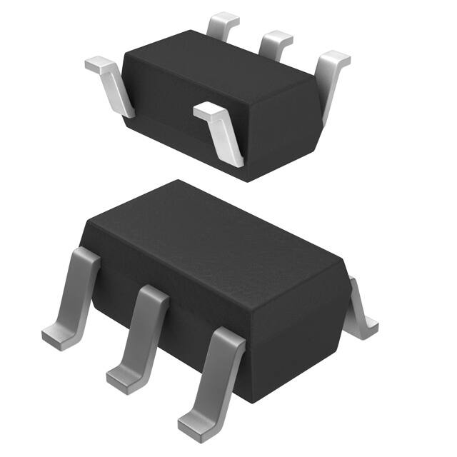
be adjusted between 1.2V and 4.8V using external resistors. The SC1563 comes in the space saving 5-pin SOT23 package.
350mV dropout @ 500mA
Designed to operate with ceramic capacitors
Adjustable output from 1.2V to 4.8V
Multiple output voltage options (all parts also
adjustable externally using resistors)
Over current and over temperature protection
2µA quiescent current in shutdown
No minimum load current requirement
Low reverse leakage (output to input)
Full industrial temperature range
5-pin SOT-23 surface mount package. Also available in Lead-free, fully WEEE and RoHS compliant
Applications
Personal Digital Assistants
Battery powered systems
Motherboards
Peripheral cards
PCMCIA cards
Typical Application Circuits
Internally Preset Output Voltage
U1
5
VIN
1
SHDN
Externally Set Output Voltage
SC1563IS-X.X
IN
OUT
4
VO (X.XV)
SHDN GND ADJ
C1
2
3
5
VIN
1
SHDN
U1
SC1563IS-X.X
IN
OUT
4
VO
R1
SHDN GND ADJ
C2
C1
2
3
C2
R2
VOUT =
Revision: January 11, 2006
1
1.200 (R1 + R2)
Volts
R2
www.semtech.com
�SC1563
POWER MANAGEMENT
Absolute Maximum Ratings
Exceeding the specifications below may result in permanent damage to the device, or device malfunction. Operation outside of the parameters
specified in the Electrical Characteristics section is not implied.
Parameter
Symbol
Maximum
Units
VIN
-0.3 to 7
V
Shutdown Voltage
VSHDN
-0.3 to VIN
V
Power Dissipation
PD
Internally Limited
W
Thermal Resistance Junction to Ambient(1)
θJA
175
°C/W
Operating Ambient Temperature Range
TA
-40 to 85
°C
Operating Junction Temperature Range
TJ
-40 to 150
°C
Storage Temperature Range
TSTG
-65 to 150
°C
Lead Temperature (Soldering) 10 sec
TLEAD
300
°C
ESD Rating
V ESD
2
kV
Input Voltage
Note:
(1) Minimum pad size.
Electrical Characteristics
Unless specified: VSHDN = 0V, Adjustable mode (VADJ > VTH(ADJ)): VIN = 2.2V to 5.5V and IOUT = 0A to 500mA,
Fixed mode (VADJ = GND): VIN = (VOUT + 0.7V) to 5.5V and IOUT = 0A to 500mA. Values in bold apply over full operating temperature range.
Parameter
Symbol
Conditions
Min
Typ
Max
Units
6.5
V
IN
Supply Voltage Range
VIN
Quiescent Current
IQ
2.2
VIN = 3.3V
85
150
µA
VIN = 6.5V, VSHDN = Open
0.01
2.00
µA
VOUT
+1%
V
OUT
Output Voltage (1)
VOUT
VIN = VOUT + 0.7V, IOUT = 10mA
(Internal Fixed Voltage)
-1%
-2%
+2%
Line Regulation(1)
REG(LINE)
VIN = (VOUT + 0.25V) to 5.5V, IOUT = 10mA
0.1
0.4
%
Load Regulation(1)
REG(LOAD)
VIN = VOUT + 0.7V
0.15
0.40
%
2006 Semtech Corp.
2
www.semtech.com
�SC1563
POWER MANAGEMENT
Electrical Characteristics
Unless specified: VSHDN = 0V, Adjustable mode (VADJ > VTH(ADJ)): VIN = 2.2V to 5.5V and IOUT = 0A to 500mA,
Fixed mode (VADJ = GND): VIN = (VOUT + 0.7V) to 5.5V and IOUT = 0A to 500mA. Values in bold apply over full operating temperature range.
Parameter
Symbol
Conditions
VD
IOUT = 2mA
Min
Typ
Max
Units
1
5
mV
OUT (Cont.)
Dropout Voltage(1)(2)
10
IOUT = 100mA
70
100
mV
150
IOUT = 250mA
175
250
mV
350
IOUT = 500mA
350
500
mV
700
Current Limit
0.5
ILIM
1.0
A
1.212
V
ADJ
Reference Voltage(1)
VREF
VIN = 2.2V, VADJ = VOUT, IOUT = 10mA
1.188
1.200
1.176
Adjust Pin Current(3)
Adjust Pin Threshold(4)
IADJ
VADJ = VREF
VTH(ADJ)
0.10
1.224
65
150
nA
0.25
0.40
V
1.5
5.0
µA
SH D N
Shutdown Pin Current
Shutdown Pin Threshold
ISHDN
VSHDN = 0V, VIN = 3.3V
VIH
VIN = 3.3V
VIL
VIN = 3.3V
1.8
V
0.4
Over Temperature Protection
High Trip Level
Hysteresis
THI
170
°C
THYST
10
°C
Notes:
(1) Low duty cycle pulse testing with Kelvin connections required.
(2) Defined as the input to output differential at which the output voltage drops to 1% below the value measured at
a differential of 0.7V for 2.5V ≤ VOUT ≤ 3.4V. Not measurable on outputs less than 2.2V due to minimum VIN constraints. See typical characteristics curves.
(3) Guaranteed by design.
(4) When VADJ exceeds this threshold, the “Sense Select” switch disconnects the internal feedback chain from the
error amplifier and connects VADJ instead.
2006 Semtech Corp.
3
www.semtech.com
�SC1563
POWER MANAGEMENT
Pin Configurations
Ordering Information
Part Number(1)(2)(3)
Top View
P ackag e
SC1563ISK-X.XTR
SC1563ISK-X.XTRT(4)
SOT-23-5
Notes:
(1) Where -X.X denotes voltage options. Available
voltages are: 1.8V, 2.5V, 2.8V, 3.0V, 3.1V and 3.3V.
(2) Output voltage can be adjusted using external
resistors, see Pin Descriptions.
(3) Only available in tape and reel packaging. A reel
contains 3000 devices.
(4) Lead free product. This product is fully WEEE and RoHS
compliant.
SOT-23-5
Marking Information
SOT-23-5
63XX = SC1563, voltage option (example: 6318 for 1.8V option)
yyww = Date code (example: 0008 for week 8 of 2000)
2006 Semtech Corp.
4
www.semtech.com
�SC1563
POWER MANAGEMENT
Block Diagram
Pin Descriptions
Pin #
Pin Name Pin Function
1
SHDN
Shutdown Input. Leavi ng thi s pi n open turns the regulator off, reduci ng the qui escent current to a
fraction of its operating value (typically < 300nA). The device will be enabled if this pin is pulled below
0.4V. Connect to GND if not being used.
2
GND
Reference ground. This pin may be used for heatsinking purposes.
3
AD J
Thi s pi n, when grounded, sets the output voltage to that set by the i nternal feedback resi stors. If
external feedback resistors are used, the output voltage will be (See Application Circuit on page 1):
VOUT =
4
OUT
5
IN
2006 Semtech Corp.
1.200 (R1 + R2)
Volts
R2
This pin is the power output of this device, sourcing up to 500mA.
Input voltage. For regulation at full load, the input to this pin must be between (VOUT + 0.7V) and 6.5V.
Minimum VIN = 2.2V.
5
www.semtech.com
�SC1563
POWER MANAGEMENT
Applications Information
Introduction
Thermal Considerations
The SC1563 is intended for applications such as
graphics cards where high current capability and very low
dropout voltage are required. It provides a very simple,
low cost solution that uses little pcb real estate.
Additional features include a shutdown pin to allow for a
very low power consumption standby mode, and a fully
adjustable output.
The power dissipation in the SC1563 is approximately
equal to the product of the output current and the input
to output voltage differential:
Component Selection
PD( MAX ) = (VIN(MAX ) − VOUT (MIN ) )• IOUT (MAX ) + VIN(MAX ) • IQ(MAX )
PD ≈ (VIN − VOUT ) • IOUT
The absolute worst-case dissipation is given by:
Input capacitor - a 1µF ceramic capacitor is
recommended. This allows for the device being some
distance from any bulk capacitance on the rail.
Additionally, input droop due to load transients is reduced,
improving load transient response. Additional capacitance
may be added if required by the application.
For a typical scenario, VIN = 3.3V ± 5%, VOUT = 2.5V and
IOUT = 500mA, therefore:
VIN(MAX) = 3.465V,
VOUT(MIN) = 2.450V and
IQ(MAX) = 150µA,
Output capacitor - a minimum bulk capacitance of 1µF,
along with a 0.1µF ceramic decoupling capacitor is
recommended. Increasing the bulk capacitance will
improve the overall transient response. The use of
multiple lower value ceramic capacitors in parallel to
achieve the desired bulk capacitance will not cause
stability issues. Although designed for use with ceramic
output capacitors, the SC1563 is extremely tolerant of
output capacitor ESR values and thus will also work
comfortably with tantalum output capacitors.
Thus PD(MAX) = 0.508W.
Using this figure, and assuming TA(MAX) = 70°C, we can
calculate the maximum thermal impedance allowable to
maintain TJ ≤ 150°C:
R TH( J− A )(MAX ) =
(T
J(MAX )
− TA (MAX ) )
PD(MAX )
=
(150 − 70) = 157°C / W
0.508
This should be achievable with the SOT-23-5 package
using pcb copper area to aid in conducting the heat away
from the device. Internal ground/power planes and air
flow will also assist in removing heat.
Noise immunity - in very electrically noisy environments,
it is recommended that 0.1µF ceramic capacitors be
placed from IN to GND and OUT to GND as close to the
device pins as possible.
External voltage selection resistors - the use of 1%
resistors, and designing for a current flow ≥ 10µA is
recommended to ensure a well regulated output (thus
R2 ≤ 120kΩ).
2006 Semtech Corp.
6
www.semtech.com
�SC1563
POWER MANAGEMENT
Typical Characteristics
Quiescent Current vs. Junction Temperature
Quiescent Current vs. Input Voltage
vs. Output Current
vs. Output Current
150
10000
VIN = 3.3V, VADJ = VOUT
VADJ = VOUT
125
IOUT = 500mA
75
1000
IOUT = 500mA
IQ (µA)
IQ (µA)
100
IOUT = 0mA
50
100
IOUT = 0mA
25
0
10
-50
-25
0
25
50
75
100
125
150
3.0
3.5
4.0
4.5
TJ (°C)
6.0
6.5
Line Regulation vs. Junction Temperature
vs. Output Current
vs. Input Voltage Change
0.40
VIN = VOUT(NOM) + 0.7V
0.4
VIN = (VOUT(NOM) + 0.25V) to 5.5V
IOUT = 10mA
0.35
0.3
REGLINE (%VOUT(NOM))
VOUT Deviation (%V OUT(NOM))
5.5
Output Voltage vs. Junction Temperature
0.5
0.2
0.1
IOUT = 0mA
0
-0.1
-0.2
IOUT = 500mA
-0.3
0.30
0.25
0.20
0.15
0.10
0.05
-0.4
0.00
-0.5
-50
-25
0
25
50
75
100
125
-50
150
-25
0
25
0.20
0.18
50
75
100
125
150
TJ (°C)
TJ (°C)
Load Regulation vs.
Dropout Voltage (IOUT = 0.5A) vs. Output
Junction Temperature
Voltage vs. Junction Temperature
700
VIN = VOUT(NOM) + 0.7V
IOUT = 0mA to 500mA
600
0.16
TJ = 150°C
500
0.14
0.12
VD (mV)
REGLOAD (%VOUT(NOM))
5.0
VIN (V)
0.10
0.08
0.06
TJ = 25°C
400
300
200
TJ = -40°C
0.04
100
0.02
0.00
0
-50
-25
0
25
50
75
100
125
150
2.2
TJ (°C)
2006 Semtech Corp.
2.4
2.6
2.8
3.0
3.2
3.4
3.6
3.8
4.0
4.2
4.4
4.6
VOUT (V)
7
www.semtech.com
�SC1563
POWER MANAGEMENT
Typical Characteristics (Cont.)
Dropout Voltage (IOUT = 0.25A) vs. Output
Dropout Voltage (IOUT = 0.1A) vs. Output
Voltage vs. Junction Temperature
Voltage vs. Junction Temperature
150
400
350
125
300
100
VD (mV)
250
VD (mV)
TJ = 150°C
TJ = 150°C
TJ = 25°C
200
150
TJ = 25°C
75
50
100
TJ = -40°C
TJ = -40°C
25
50
0
0
2.2
2.4
2.6
2.8
3.0
3.2
3.4
3.6
3.8
4.0
4.2
4.4
2.2
4.6
2.4
2.6
2.8
3.0
3.2
4.2
4.4
Temperature vs. Output Current
4.6
VIN = 2.2V
1.204
900
1.203
850
1.202
800
1.201
VREF (V)
ILIM (mA)
4.0
Junction Temperature
750
700
IOUT = 0mA
1.200
1.199
650
1.198
600
1.197
550
1.196
IOUT = 500mA
1.195
500
-50
-25
0
25
50
75
100
125
-50
150
-25
0
25
50
75
Reference Voltage (VIN = 5.5V) vs. Junction
Adjust Pin Current vs.
Temperature vs. Output Current
Junction Temperature
1.210
1.208
100
125
150
100
125
150
TJ (°C)
TJ (°C)
100
VIN = 5.5V
90
1.206
VIN = 6.5V
VADJ = VREF
80
1.204
70
IOUT = 0mA
1.202
IADJ (nA)
VREF (V)
3.8
Reference Voltage (VIN = 2.2V) vs. Junction
VIN = VOUT(NOM) + 0.7V
950
3.6
Current Limit vs.
1.205
1000
3.4
VOUT (V)
VOUT (V)
1.200
1.198
1.196
50
40
30
IOUT = 500mA
1.194
60
20
1.192
10
1.190
0
-50
-25
0
25
50
75
100
125
150
-50
TJ (°C)
2006 Semtech Corp.
-25
0
25
50
75
TJ (°C)
8
www.semtech.com
�SC1563
POWER MANAGEMENT
Typical Characteristics (Cont.)
Adjust Pin Threshold Voltage
Shutdown Pin Current vs.
vs. Junction Temperature
Junction Temperature
2.50
400
2.2V ≤ VIN ≤ 6.5V
375
350
2.00
325
1.75
300
ISHDN (µA)
VTH(ADJ) (mV)
VIN = 3.3V
VSHDN = 0V
2.25
275
250
225
200
1.50
1.25
1.00
0.75
175
0.50
150
0.25
125
0.00
100
-50
-25
0
25
50
75
100
125
-50
150
-25
0
25
50
75
100
125
150
TJ (°C)
TJ (°C)
Shutdown Pin Threshold Voltage vs. Junction
Temperature vs. Input Voltage
1.8
1.6
VIH, VIN = 6.5V
VIH, VIL (V)
1.4
1.2
VIL, VIN = 6.5V
1.0
VIH, VIN = 2.2V
0.8
0.6
VIL, VIN = 2.2V
0.4
-50
-25
0
25
50
75
100
125
150
TJ (°C)
2006 Semtech Corp.
9
www.semtech.com
�SC1563
POWER MANAGEMENT
Outline Drawing - SOT-23-5
A
DIM
e1
2X E/2
D
A
A1
A2
b
c
D
E1
E
e
e1
L
L1
N
01
aaa
bbb
ccc
N
EI
1
E
2
ccc
2X N/2 TIPS
e
B
D
aaa C
A2
DIMENSIONS
INCHES
MILLIMETERS
MIN NOM MAX MIN NOM MAX
.035
.000
.035
.010
.003
.110
.060
-
.045
-
.057
.006
.051
.020
.009
.118
.069
.114
.063
.110 BSC
.037 BSC
.075 BSC
.012 .018 .024
(.024)
5
0°
10°
.004
.008
.008
0.90
0.00
.90
0.25
0.08
2.80
1.50
-
1.15
-
1.45
0.15
1.30
0.50
0.22
3.00
1.75
2.90
1.60
2.80 BSC
0.95 BSC
1.90 BSC
0.30 0.45 0.60
(0.60)
5
0°
10°
0.10
0.20
0.20
A
SEATING PLANE
A1
C
H
bxN
bbb
C A-B D
c
GAGE
PLANE
0.25
L
01
(L1)
SEE DETAIL
DETAIL
A
A
SIDE VIEW
NOTES:
1.
CONTROLLING DIMENSIONS ARE IN MILLIMETERS (ANGLES IN DEGREES).
2. DATUMS -A- AND -B- TO BE DETERMINED AT DATUM PLANE -H3. DIMENSIONS "E1" AND "D" DO NOT INCLUDE MOLD FLASH, PROTRUSIONS
OR GATE BURRS.
Land Pattern - SOT-23-5
X
DIM
(C)
G
Z
Y
P
C
G
P
X
Y
Z
DIMENSIONS
MILLIMETERS
INCHES
(.098)
.055
.037
.024
.043
.141
(2.50)
1.40
0.95
0.60
1.10
3.60
NOTES:
1.
THIS LAND PATTERN IS FOR REFERENCE PURPOSES ONLY.
CONSULT YOUR MANUFACTURING GROUP TO ENSURE YOUR
COMPANY'S MANUFACTURING GUIDELINES ARE MET.
Contact Information
Semtech Corporation
Power Management Products Division
200 Flynn Road, Camarillo, CA 93012
Phone: (805)498-2111 FAX (805)498-3804
2006 Semtech Corp.
10
www.semtech.com
�