SC2620
Dual 2A, 30V Step-down Regulator with
Programmable Frequency up to 1.4MHz
POWER MANAGEMENT
Description
Features
The SC2620 is a constant frequency dual current-mode
switching regulator with integrated 2.3A, 30V switches.
Its switching frequency can be programmed up to 1.4MHz
per channel. Due to the SC2620’s high frequency
operation, small inductors and ceramic capacitors can be
used, resulting in very compact power supplies. The two
channels of the SC2620 operate at 180° out of phase for
reduced input voltage ripples.
u Wide Input Voltage Range 2.8V to 30V
u Up to 1.4MHz/Channel Programmable Switching
u
u
u
u
u
Separate soft start/enable pins allow independent control u
of each channel. Channel 1 power good indicator can be u
used for output start up sequencing to prevent latch-up. u
u
Current-mode PWM control achieves fast transient u
response with simple loop compensation. Cycle-by-cycle
current limiting and hiccup overload protection reduce
power dissipation during overload.
Frequency
Current-mode Control
Out of Phase Switching Reduces Ripple
Cycle-by-cycle Current-limiting
Independent Shutdown/soft-start Pins
Independent Hiccup Overload Protection
Channel 1 Power Good Indicator
Two 2.3A Integrated Switches
Thermal Shutdown
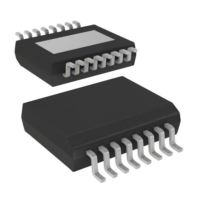
Thermally Enhanced SO-16 Lead Free Package
Fully WEEE and RoHS Compliant
Applications
u
u
u
u
u
XDSL and Cable Modems
Set-top Boxes
Point of Load Applications
CPE Equipment
DSP Power Supplies
Typical Application Circuit
C5
R5
12.7k C6 1.5nF
COMP1
D3
FB1
BOOST1
C7 47pF
22nF
SW1
R9
9V-16V VIN
ROSC
46.4k
C15
SC2620
PGOOD1
3.3V/2A
R1
30.1k
C1
22µF
R10 10µF
10
SS2
CH1
OUT1
10µH
D1
UPS120
PVIN
C10
CH2
R2
13k
VIN
22nF
C16
0.1µF
C9
COMP2
SW2
OUT2
6.8µH
D4
1N4148
4.7nF
FB2
CH3
D2
UPS120
L2
R7 33pF C8
10.5k
V IN = 12V
C2
1N4148
0.1µF
L1
SS1
R3 1.2V/2A
2.61k
C4
0.1µF
C3
22µF
BOOST2
GND
L1 & L2: Coiltr onics DR73
R4
13k
CH1 : OUT1 Voltage, 2V/div
CH2 : OUT2 Voltage, 1V/div
CH3 : SS2 Voltage, 2V/div
C1 & C3: Murata GRM21BR60J 226M
C15: Murata GRM32DR61E106K
Figure 1(a). 550kHz 9V-16V VIN to 3.3V and 1.2V Stepdown Converter.
Revision: March 25, 2009
4ms/div
Figure 1(b). VIN Start-up Transient (IOUT1= 1.5A, IOUT2=
0.8A). Channel 2 start is delayed until
Channel 1 reaches regulation.
1
www.semtech.com
�SC2620
POWER MANAGEMENT
Absolute Maximum Ratings
Exceeding the specifications below may result in permanent damage to the device, or device malfunction. Operation outside of the parameters specified in the
Electrical Characteristics section is not implied.
Parameter
Symbol
Max
Units
V IN
-0.3 to 32
V
VBST
42
V
Boost Pin Above SW
V BST-V SW
24
V
PGOOD1 Pin Voltage
VPGOOD1
V IN
V
SS Pins
VSS
3
V
FB Pins
V FB
-0.3 to VIN
V
SW Voltage
VSW
-0.6 to VIN
V
Thermal Resistance Junction to Ambient
θJA
31
°C/W
Thermal Resistance Junction to Case
θJC
3.9
°C/W
Maximum Junction Temperature
TJ
150
°C
TSTG
-65 to +150
°C
TP
260
°C
Lead Temperature (Soldering)10 sec
TLEAD
300
°C
ESD Rating (Human Body Model) (Note 1)
ESD
1.5
kV
Input Voltage
Boost Pin
Storage Temperature Range
IR Reflow Temperature
Note 1: This device is ESD sensitive. Standard ESD handling precaution is required.
Recommended Operating Conditions
The Performance is not guaranteed if exceeding the specifications below
Parameter
Symbol
Conditions
Min
Typ
Max
Units
Input Voltage Range
VIN
2.8
30
V
Ambient Temperature Range
TA
-40
105
°C
Junction Temperature
TJ
-40
125
°C
Electrical Characteristics
Unless specified: -40°C < TJ< 125°C, ROSC = 12.1kΩ, VIN = 5V, VBOOST = 8V
Parameter
Conditions
VIN Start Voltage
Min
Typ
Max
Units
2.45
2.62
2.78
V
VIN Start Hysteresis
75
mV
Quiescent Current
Not switching, PGOOD1 Open
3.5
5
mA
Shutdown Current
V SS1=V SS2=0, PGOOD1 Open
40
60
µA
1.000
1.020
V
Feedback Voltage
0.980
Feedback Voltage Lin Regulation
Vin=3V to 30V
FB Pin Input Bias Current
V FB=1V, VCOMP=1.5V
2008 Semtech Corp.
0.005
-15
2
%/V
-30
nA
www.semtech.com
�SC2620
POWER MANAGEMENT
Electrical Characteristics (Cont.)
Unless specified: -40°C < TJ< 125°C, ROSC = 12.1kΩ, VIN = 5V, VBOOST = 8V
Parameter
Min
Conditions
Typ
Max
Units
Error Amplifier Transconductance
280
µΩ-1
Error Amplifier Open-Loop Gain
53
dB
COMP Source Current
VFB = 0.8V, VCOMP = 1.5V
20
µA
COMP Sink Current
VFB = 1.2V, VCOMP = 1.5V
20
µA
8
A/V
COMP Pin to Switch Current Gain
COMP Switching Threshold
COMP Maximum Voltage
0.7
1.1
1.3
2.4
VFB = 0.9V
Channel Switching Frequency
1.2
1.4
V
V
1.6
MHz
Maximum Duty Cycle
(Note 3)
80
90
%
Switch Current Limit
(Notes 2 and 4)
2.3
3.2
A
Switch Saturation Voltage
ISW = -2A
0.3
V
Switch Leakage Current
Minimum Boost Voltage
Boost Pin Current
Minimum Soft-Start Voltage to Exit
Shutdown
10
µA
2.5
V
ISW = -2A (Note 2)
1.8
ISW = -0.5A
20
mA
ISW = -2A
60
mA
SS1 Tied to SS2
0.2
0.4
0.7
V
2
µA
VSS = 1.5V
1.8
µA
Soft-start Discharging Current
VSS = 1.5V
0.8
µA
Minimum Soft-start Voltage to
Enable Overload Shutoff
VSS Rising
2
V
FB Overload Threshold
VSS = 2.3V, VFB Falling
0.7
V
Soft-start Voltage to Restart
Switching After Overload Shutoff
VSS Falling
0.7
1
1.3
V
Power Good Threshold Below FB1
VFB1 Rising
80
100
120
mV
Power Good Output Low Voltage
VFB1 = 0.8V, IPGOOD1 = 250µA
0.2
0.4
V
Power Good Pin Leakage Current
VPGOOD1 = 5V
0.1
1
µA
Soft-start Charging Current
VSS = 0V
Thermal Shutdown Temperature
155
°C
Thermal Shutdown Hysteresis
10
°C
Note 2: Guaranteed by design, not 100% tested in production.
Note 3: The maximum duty cycle specified corresponds to 1.4MHz switching frequency. Duty cycles higher than those specified can be achieved
by lowering the operating frequency.
Note 4: Switch current limit does not vary with duty cycle.
2008 Semtech Corp.
3
www.semtech.com
�SC2620
POWER MANAGEMENT
Pin Configuration
Ordering Information
TOP VIEW
FB1
1
16
COMP1
BOOST1
2
15
PGOOD1
SW1
3
14
SS1
PVIN1
4
13
ROSC
PVIN2
5
12
VIN
SW2
6
11
GND
BOOST2
7
10
SS2
FB2
8
9
Part Number
Package
SC2620SETRT(1)(2)
SOIC-16 EDP
SC2620EVB
Evaluation Board
Notes:
(1) Only available in tape and reel packaging. A reel contains
2500 devices.
(2) Lead free product. This product is fully WEEE and RoHS
compliant.
COMP2
(16 Pin SOIC-EDP)
Underside metal must be soldered to ground.
Pin Descriptions
Pin #
Pin Name
Pin Function
1, 8
FB1, FB2
The inverting inputs of the error amplifiers. Each FB pin is tied to a resistive divider between its
output and ground to set the channel output voltage.
2, 7
BOOST1,
BOOST2
Supply pins to the power transistor drivers. Tie to external diode-capacitor charge pumps to
generate drive voltages higher than V IN in order to fully enhance the internal NPN power switches.
3, 6
SW1, SW2
Emitters of the internal power NPN transistors. Each SW pin is connected to the corresponding
inductor, freewheeling diode and bootstrap capacitor.
4, 5
Collectors of the internal power transistors and the power supplies to the corresponding current
PVIN1, PVIN2 sensing circuits. Pins 4 and 5 are not internally connected. They must be joined on the PCB and
closely bypassed to the power ground plane.
COMP1,
COMP2
Outputs of the internal error amplifiers. The voltages at these pins control the peak switch
currents. RC networks at these pins stabilize the control loops. Pulling either pin below 0.7V
stops the corresponding switching regulator.
10, 14
SS1, SS2
A capacitor from either SS pin to ground provides soft-start and overload hiccup functions for
that channel. Pulling either SS pin below 0.8V with an open drain or collector transistor shuts off
the corresponding regulator. To completely shut off the SC2620 to low-current state, pull both SS
pins to ground. Soft-start is recommended for all applications.
11
GND
12
VIN
Power supply to the analog control section of the SC2620. Connect to the PVIN pins through an
optional RC filter.
13
ROSC
An external resistor between this pin and the analog ground sets the channel switching frequency.
PGOOD1
Open collector output of Channel 1 power good comparator. Tie to an external pull-up resistor
from the input or the output of the converter. PGOOD1 output becomes valid as soon as V IN rises
above 1 VBE during power-up. PGOOD1 is actively pulled low until FB1 voltage rises to within
10% of its final regulation voltage.
9, 16
15
Underside
Metal
2008 Semtech Corp.
Analog ground. Connect to the PCB power ground plane at a single point.
The exposed pad at the bottom of the package is electrically connected to the ground pin of the
SC2620. It also serves as a thermal contact to the circuit board. It is to be soldered to the analog
ground plane of the PC board.
4
www.semtech.com
�SC2620
POWER MANAGEMENT
Block Diagrams
4 PVIN1
PGOOD1
Σ
15
CHANNEL 1 ONLY
+
ISEN
-
+
+
-
6.3mΩ
SLOPE
COMP 1
+
+
ILIM
-
POWER
GOOD
100mV
COMP1
20mV
BOOST1
2
16
FB1
+
PWM
-
-
1
EA
S
Q
POWER
TRANSISTOR
R
+
SS1
14
FB1
3
1V
REFERENCE
& THERMAL
SHUTDOWN
SS2
10
Soft-Start
And
Overload
Hiccup
Control 1
0.7V
FAULT
SW1
OVLD
12 VIN
SLOPE
COMP 1
SLOPE COMP
ROSC
13
SLOPE
COMP 2
CLK1
FREQUENCY
CLK2
DIVIDER
OSCILLATOR
11 GND
Figure 2. SC2620 Block Diagram (Channel 1)
FB
0.7V
SS
+
-
S
Q
1.8µA
OVLD
R
1V/2V
FAULT
2.6µA
Figure 3. Details of the Soft-Start and Overload Hiccup Control Circuit
2008 Semtech Corp.
5
www.semtech.com
�SC2620
POWER MANAGEMENT
Typical Characteristics
Frequency Setting Resistor
vs Channel Frequency
Feedback Voltage vs Temperature
1.02
1.10
1000
VIN = 5V
VIN = 5V
1.00
0.99
Normalized Frequency
ROSC (k Ω )
1.01
VFB (V)
Normalized Channel
Frequency vs Temperature
100
0.98
0.97
-25
0
25
50
75
0.0
100 125
0.5
1.0
-50
1.5
-25
0
25
50
75
100 125
Temperature (°C)
Boost Pin Current
vs Switch Current
80
3.6
V IN = 5V
125°C
-40°C
200
Boost Pin Current (mA)
3.4
Current Limit (A)
VCESAT (mV)
0.95
Switch Current Limit
vs Temperature
Switch Saturation Voltage
vs Switch Current
300
1.4MHz
Frequency (M Hz)
Temperature (°C)
400
1.00
0.90
10
-50
600kHz
1.05
3.2
3.0
2.8
V BST = 8V
60
-40°C
40
125°C
20
25°C
100
0
2.6
0.0
0.5
1.0
1.5
2.0
2.5
-50
-25
0
25
50
0.0
100 125
Temperature (°C)
SS Shutdown Threshold
vs Temperature
V IN Shutdown Current vs V IN
VSS1 = VSS2
100
2
1
TA = 25°C
VSS1 = VSS2 = 0
0
0
-50 -25
0
25
50
75 100 125
Tempe rature (°C)
2008 Semtech Corp.
2.5
3
150
50
0.20
2.0
VIN Quiescent Current vs VIN
V IN Current (mA)
0.25
1.5
TA = 25°C
VIN Current (PA)
0.30
1.0
4
200
0.35
0.5
Switch Current (A)
Switch Current (A)
0.40
SS Threshold (V)
75
0
5
10
15
VIN (V)
6
20
25
30
0
5
10
15
20
25
30
VIN (V)
www.semtech.com
�SC2620
POWER MANAGEMENT
Typical Characteristics
VIN Supply Current
vs Soft-Start Voltage
Soft-Start Pin Current
vs Soft-Start Voltage
0
1.0
4
TA = 25°C
T = 25°C
VIN =5V
-40
-60
I IN (mA)
ISS of the
Swept Channel
0.9
3
FB Threshold (V)
-20
ISS (µ A)
FB Overload Threshold
vs Temperature
2
V IN = 5V
-80
VSS1 = V SS2
1
-100
ISS of the Other
V COMP1 = 0
Channel (V SS = 0)
V COMP2 = 0
0.0
0.5
1.0
1.5
0.5
0.0
2.0
0.7
0.6
0
-120
0.8
0.5
1.0
1.5
2.0
V SS (V)
VSS (V)
PGOOD1 Threshold to VFB
Difference Voltage vs Temperature
-50
-25
0
25
50
75
100 125
Temperature (°C)
Efficiency vs Load Current
-90
90
85
VOUT1 = 3.3V
80
Efficiency (%)
Voltage (mV )
-92
-94
-96
75
70
65
VOUT2 = 1.2V
60
55
-98
50
45
-100
Figure 1(a), VIN=12V
40
-50
-25
0
25
50
75
Temperature (°C)
2008 Semtech Corp.
100 125
0
0.5
1
1.5
2
Load Current (A)
7
www.semtech.com
�SC2620
POWER MANAGEMENT
Operation
The SC2620 is a 30V 2-channel constant-frequency peak
current-mode step-down switching regulator with integrated
2.3A power transistors. Both regulators in the SC2620
operate from a common input power supply and share the
same voltage reference and the master oscillator. Turn-on
of the power transistors is phase-shifted by 180°. The two
regulator cores are otherwise completely identical,
independent and are capable of producing two separate
outputs from the same input.
regulator. When either SS pin is pulled below 0.8V, that
regulator is turned off. If both SS pins are pulled below
0.2V, then the SC2620 undergoes overall shutdown. The
current drawn from the input power supply reduces to
40µA. When either SS pin is released, the corresponding
soft-start capacitor is charged with a 2µA current source
(not shown in Figure 3). As either SS voltage exceeds 0.3V,
the internal bias circuit of the SC2620 is enabled. The
SC2620 draws 3.5mA from VIN. An internal fast charge
circuit quickly charges the soft-start capacitor to 1V. At
this juncture, the fast charge circuit turns off and the 1.8µA
current source slowly charges the soft-start capacitor. The
output of the error amplifier is forced to track the slow
soft-start ramp at the SS pin. When the COMP voltage
exceeds 1.1V, the switching regulator starts to switch.
During soft-start, the current limit of the converter is
gradually increased until the converter output comes into
regulation.
The channel frequency can be programmed with an
external resistor from the ROSC pin to ground. This allows
the designer to set the switching frequency according to
the input to the output voltage conversion ratio.
Peak current-mode control is utilized for the SC2620. The
double reactive poles of the output LC filter are reduced to
a single real pole by the inner current loop, easing loop
compensation. Fast transient response can be achieved
with a simple Type-2 compensation network. Switch
collector current is sensed with an integrated 6.3mΩ sense
resistor. The sensed current is summed with slopecompensating ramp before it is compared with the
transconductance error amplifier output. The PWM
comparator tripping point determines the switch turn-on
pulse width (Figure 2). The current-limit comparator ILIM
turns off the power switch when the sensed-signal exceeds
the 20mV current-limit threshold. ILIM therefore provides
cycle-by-cycle limit. Current-limit does not vary with dutycycle.
Hiccup overload protection is utilized in the SC2620.
Overload shutdown is disabled during soft-start (VSS < 2V).
In Figure 3 the reset input of the overload latch will remain
high if the SS voltage is below 2V. Once the soft-start
capacitor is charged above 2V, the overload shutdown latch
is enabled. As the load draws more current from the
regulator, the current-limit comparator will limit the peak
inductor current. This is cycle-by-cycle current limiting.
Further increase in load current will cause the output
voltage to decrease. If the output voltage falls below 70%
of its set point, then the overload latch will be set and the
soft-start capacitor will be discharged with a net current
of 0.8µA. The switching regulator is shut off until the softstart capacitor is discharged below 1V. At this moment,
the overload latch is reset. The soft-start capacitor is
recharged and the converter again undergoes soft-start.
The regulator will go through soft-start, overload shutdown
and restart until it is no longer overloaded.
An external charge pump (formed by the capacitor C2 and
the diode D3 in Figure 1(a)) generates a voltage higher
than the input rail at the BOOST pin. The bootstrapped
voltage generated becomes the supply voltage for the
power transistor driver. Driving the base of the power
transistor above the input power supply rail minimizes the
power transistor turn-on voltage and maximizes efficiency.
The power good comparator indicates that the channel 1
regulator output has risen to within 10% of its set value.
The open collector output of the power good comparator
will be actively pulled low if its feedback voltage is below
0.9V.
The SS pin is a multiple-function pin. An external capacitor
connected from the SS pin to ground together with the
internal 1.8µA and 2.6µA current sources set the softstart and overload shutoff times of the regulator (Figure
3). The SS pin can also be used to shut off the corresponding
2008 Semtech Corp.
8
www.semtech.com
�SC2620
POWER MANAGEMENT
Applications Information
Setting the Output Voltage
Channel switching frequency is limited by the minimum
controllable on time at low duty cycles. For VIN > 20V, setting
the switching frequency below 500kHz makes converter
output short circuit operation more robust. These will be
described in more details later.
The regulator output voltage is set with an external resistive
divider (Figure 4) with its center tap tied to the FB pin.
VOUT
Minimum On Time Consideration
R1
15nA
SC2620
The operating duty cycle of a non-synchronous step-down
switching regulator in continuous-conduction mode (CCM)
is given by
FB
R2
D=
Figure 4. VOUT is set with a Resistive Divider
R1 = R2 (VOUT − 1)
VOUT + VD
VIN + VD − VCESAT
(2)
where VCESAT is the switch saturation voltage and VD is
voltage drop across the rectifying diode.
(1)
The percentage error due the input bias current of the
error amplifier is
VIN
ratio. In peak
VOUT
Duty cycle decreases with increasing
∆VOUT − 15nA ⋅ 100 ⋅ (R1R2 )
=
.
VOUT
1V
current-mode control, the PWM modulating ramp is the
sensed current ramp of the power switch. This current
ramp is absent unless the switch is turned on. The
intersection of this ramp with the output of the voltage
feedback error amplifier determines the switch pulse width.
The propagation delay time required to immediately turn
off the switch after it is turned on is the minimum
controllable switch on time (T ON (MIN) ). Closed-loop
Example: Determine the output voltage error of a
VOUT = 5 V converter with R 2 = 51.1kΩ .
From (1),
R1 = 51.1kΩ ⋅ (5 − 1) = 205kΩ
measurement of the SC2620 with low
∆VOUT − 15nA ⋅ 100 ⋅ (51.1k205k)
=
= −0.061% .
VOUT
1V
VOUT
ratios shows
VIN
Minimum On Time
vs Ambient Temperature
130
This error is at least an order of magnitude lower than the
ratio tolerance resulting from the use of 1% resistors in the
divider string.
TON(MIN) (ns)
120
Setting the Channel Frequency
The switching frequency of the master oscillator is set with
an external resistor from the ROSC pin to ground. Channel
frequency is one-half of that of the master oscillator. A
graph of channel frequency against ROSC is shown in the
“Typical Performance Characteristics”. Channel frequency
is programmable up to 1.4MHz.
2008 Semtech Corp.
110
100
90
80
-50
-25
0
25
50
75
100
Temperature (°C)
Figure 5. Variation of Minimum On Time with
Ambient Temperature.
9
www.semtech.com
�SC2620
POWER MANAGEMENT
Applications Information
that the minimum on time is about 105ns at room
temperature (Figure 5). The power switch in the SC2620
is either not turned on at all or for at least TON(MIN). If the
Example: Determine the maximum operating frequency of
a dual 5V to 1.5V and 5V to 4V switching regulator using
the SC2620.
D
) is shorter than the minimum
f
on time, the regulator will either skip cycles or it will jitter.
Assuming that VD = 0.45V, VCESAT = 0.25V and VIN = 4.5V
required switch on time (=
(10% low line), the duty ratios D1 and D 2 of the 1.5V and
4V converters can be calculated using (2).
Example: Determine the maximum operating frequency
of a dual 24V to 1.2V and 24V to 3.3V switching regulator
using the SC2620.
Assuming that VD = 0.45V, VCESAT = 0.25V and VIN = 26.4V
(10% high line), the corresponding duty ratios, D1 and D2,
of the 1.2V and 3.3V converters can be calculated using
(2).
D1 =
1.5 + 0.45
= 0.42
4.5 + 0.45 − 0.25
D2 =
4 + 0.45
= 0.95 .
4.5 + 0.45 − 0.25
The maximum operating channel frequency of the dual
1.2 + 0.45
= 0.062
D1 =
26.4 + 0.45 − 0.25
D2 =
1.5V and the 4V converter is therefore
3.3 + 0.45
= 0.14
26.4 + 0.45 − 0.25
Transient headroom requires that channel frequency be
lower than 410kHz.
To allow for transient headroom, the minimum operating
switch on time should be at least 30% higher than the
worst-case minimum on time exhibited in Figure 5.
Designing for a switch on time of 150ns at VIN = 26.4 V ,
the maximum operating frequency of the 24V to 1.2V and
3.3V converter is
1 − D2
= 410kHz .
120ns
Inductor Selection
The inductor ripple current ∆IL for a non-synchronous stepdown converter in continuous-conduction mode is
D1
= 410kHz .
150ns
∆IL =
( VOUT + VD )(1 − D) ( VOUT + VD )( VIN − VOUT − VCESAT )
=
fL
( VIN + VD − VCESAT ) fL
(3)
Minimum Off Time Limitation
where f is the switching frequency and L is the inductance.
The PWM latch in Figure 2 is reset every period by the
clock. The clock also turns off the power transistor to refresh
the bootstrap capacitor. This minimum off time limits the
attainable duty cycle of the regulator at a given switching
frequency. The measured minimum off time is 120ns. For
a step-down converter, D increases with increasing
In current-mode control, the slope of the modulating
(sensed switch current) ramp should be steep enough to
lessen jittery tendency but not so steep that large flux
swing decreases efficiency. Inductor ripple current ∆IL
between 25-40% of the peak inductor current limit is a
good compromise. Inductors so chosen are optimized in
size and DCR. Setting ∆IL = 0.3(2.3) = 0.69 A ,
VOUT
VIN
ratio. If the required duty cycle is higher than the attainable
maximum, then the output voltage will not be able to reach
its set value in continuous-conduction mode.
2008 Semtech Corp.
VD = 0.45 V and VCESAT = 0.25 V in (3),
10
www.semtech.com
�SC2620
POWER MANAGEMENT
Applications Information
( V + 0.45)( VIn − VOUT − 0.25)
L = OUT
( VIN + 0.2)(0.69) f
2
Power dissipated in the input capacitor is IRMS( CIN) ⋅ (ESR) .
(4)
where L is in µH and f is in MHz.
IOUT
1
( at D = ),
2
2
corresponding to the worst-case power dissipation
Equation (3) shows that for a given VOUT , ∆IL increases as
I2OUT ⋅ ESR
in CIN.
4
Equation (6) has a maximum value of
D decreases. If VIN varies over a wide range, then choose
L based on the nominal input voltage. Always verify
converter operation at the input voltage extremes.
A dual-channel step-down converter with interleaved
switching reduces the RMS ripple current in the input
capacitor to a fraction of that of a single-phase buck
converter. If both power transistors in the SC2620 were
to switch on in phase, the current drawn by the SC2620
would consist of current pulses with amplitude equal to
the sum of the channel output currents. If each channel
were delivering IOUT and operating at 50% duty cycle, then
the input current would switch from zero to 2IOUT. The RMS
ripple current in the input capacitor would then be IOUT.
The peak current limits of both SC2620 power transistors
are internally set at 3.2A. The peak current limits are dutycycle invariant and are guaranteed higher than 2.3A. The
maximum load current is therefore conservatively:
IOUT (MAX ) = ILM −
∆IL
∆I
= 2 .3 A − L
2
2
(5)
Power dissipated in CIN would be I2OUT ⋅ ESR , 4 times that
of a single-channel converter. The SC2620 produces the
highest RMS ripple current in CIN when only one channel is
running and delivering the maximum output current (2A).
The input capacitor therefore should have a RMS ripple
current rating of at least 1A.
If ∆IL = 0.3 ⋅ ILM , then
IOUT(MAX ) = ILM −
∆IL
0.3ILM
= ILM −
= 0.85 ⋅ ILM .
2
2
The saturation current of the inductor should be 20-30%
higher than the peak current limit (2.3A). Low-cost powder
iron cores are not suitable for high-frequency switching
power supplies due to their high core losses. Inductors
with ferrite cores should be used.
Multi-layer ceramic capacitors, which have very low ESR
(a few mΩ) and can easily handle high RMS ripple current,
are the ideal choice for input filtering. A single 4.7µF or
10µF X5R ceramic capacitor is adequate. For high voltage
applications, a small ceramic (1µF or 2.2µF) can be placed
in parallel with a low ESR electrolytic capacitor to satisfy
both the ESR and bulk capacitance requirements.
Power Line Input Capacitor
A buck converter draws pulse current with peak-to-peak
amplitude equal to its output current IOUT from its input
supply. An input capacitor placed between the supply and
the buck converter filters the AC current and keeps the
current drawn from the supply to a DC constant. The input
capacitance CIN should be high enough to filter the pulse
input current. Its equivalent series resistance (ESR) should
be low so that power dissipated in the capacitor does not
result in significant temperature rise and degrade reliability.
For a single channel buck converter, the RMS ripple current
in the input capacitor is
IRMS( CIN) = IOUT D(1 − D) .
2008 Semtech Corp.
Output Capacitor
The output ripple voltage ∆VOUT of a buck converter can be
expressed as
1
∆VOUT = ∆IL ESR +
8 fCOUT
(7)
where COUT is the output capacitance.
Inductor ripple current ∆IL increases as D decreases
(Equation (3)). The output ripple voltage is therefore the
highest when VIN is at its maximum. The first term in (7)
results from the ESR of the output capacitor while the
(6)
11
www.semtech.com
�SC2620
POWER MANAGEMENT
Applications Information
their bases will have to be driven from a power supply
higher in voltage than VIN. The required driver supply
voltage (at least 2.5V higher than the SW voltage over the
industrial temperature range) is generated with a bootstrap
circuit (the diode DBST and the capacitor CBST in Figure 7).
second term is due to the charging and discharging of
COUT by the inductor ripple current. Substituting ∆IL =
0.69A, f = 500kHz and COUT = 22µF ceramic with ESR =
2mΩ in (7),
∆VOUT = 0.69 A ⋅ (2mΩ + 11.4mΩ)
= 1.4mV + 7.8mV = 9.2mV
The bootstrapped output (the common node between DBST
and CBST) is connected to the BOOST pin of the SC2620.
The power transistor in the SC2620 is first switched on to
build up current in the inductor. When the transistor is
switched off, the inductor current pulls the SW node low,
allowing CBST to be charged through DBST. When the power
switch is again turned on, the SW voltage goes high. This
brings the BOOST voltage to VSW + VC BST , thus back-biasing
Depending on operating frequency and the type of
capacitor, ripple voltage resulting from charging and
discharging of COUT may be higer than that due to ESR. A
10µF to 47µF X5R ceramic capacitor is found adequate
for output filtering in most applications. Ripple current in
the output capacitor is not a concern because the inductor
current of a buck converter directly feeds COUT, resulting in
very low ripple current. Avoid using Z5U and Y5V ceramic
capacitors for output filtering because these types of
capacitors have high temperature and high voltage
coefficients.
DBST. CBST voltage increases with each subsequent switching
cycle, as does the bootstrapped voltage at the BOOST pin.
After a number of switching cycles, CBST will be fully charged
to a voltage approximately equal to that applied to the
anode of D BST. Figure 6 shows the typical minimum BOOST
to SW voltage required to fully saturate the power transistor.
This differential voltage ( = VC BST ) must be at least 1.8V at
Freewheeling Diode
Use of Schottky barrier diodes as freewheeling rectifiers
reduces diode reverse recovery input current spikes, easing
high-side current sensing in the SC2620. These diodes
should have an average forward current rating between
1A and 2A and a reverse blocking voltage of at least a few
volts higher than the input voltage. For switching regulators
operating at low duty cycles (i.e. low output voltage to
input voltage conversion ratios), it is beneficial to use
freewheeling diodes with somewhat higher average current
ratings (thus lower forward voltages). This is because the
diode conduction interval is much longer than that of the
transistor. Converter efficiency will be improved if the
voltage drop across the diode is lower.
room temperature. This is also specified in the “Electrical
Characteristics” as “Minimum Bootstrap Voltage”. The
minimum required V C BST increases as temperature
decreases. The bootstrap circuit reaches equilibrium when
the base charge drawn from C BST during transistor on time
is equal to the charge replenished during the off interval.
Minimum Bootstrap Voltage
vs Temperature
2.4
2.2
Voltage (V)
The freewheeling diodes should be placed close to the SW
pins of the SC2620 to minimize ringing due to trace
inductance. 10BQ015, 20BQ030 (International Rectifier),
MBRM120LT3 (ON Semi), UPS120 and UPS140 (MicroSemi) are all suitable.
1.8
1.6
Bootstrapping the Power Transistors
1.4
-50
To maximize efficiency, the turn-on voltage across the
internal power NPN transistors should be minimized. If
these transistors are to be driven into saturation, then
2008 Semtech Corp.
2.0
-25
0
25
50
75
100
Temperature (°C)
Figure 6. Typical Minimum Bootstrap Voltage Required to Maintain Saturation at ISW = 2A.
12
www.semtech.com
�SC2620
POWER MANAGEMENT
Applications Information
ISW
I
≈ SW , where ISW and β
â+1 â
are the switch emitter current and current gain respectively,
refreshed to VA − VDBST + VDRECT every cycle, where VA is the
applied DBST anode voltage. Switch base current discharges
The switch base current =
the bootstrap capacitor to VA − VDBST + VDRECT −
I T
is drawn from the bootstrap capacitor CBST. Charge SW ON
â
is drawn from CBST during the switch on time, resulting in a
voltage droop of
end of conduction. This voltage must be higher than the
minimum shown in Figure 6 to ensure full switch
enhancement. DBST can be tied either to the input or to
the output of the DC/DC converter.
I SW TON
. If ISW = 2A, TON = 1µs, β = 35 and
âCBST
CBST = 0.1µF, then the VCBST droop will be 0.57V. CBSTT is
MAX VBST = VIN + VOUT
BOOST
If DBST is tied to the input, then the charge drawn from the
DBST
DBST
VOUT
IN
MAX VBST = 2VIN
BOOST
CBST
VIN
VOUT
IN
SC2620
SW
SC2620
D RECT
(b)
MAX VBST = 2VIN - VZ
DZ
DRECT
GND
(a)
DBST
CBST
VIN
SW
GND
ISW TON
at the
βCBST
MAX VBST = VIN + V S
DBST
VS > 2.5V
+ VZ BOOST
BOOST
CBST
VIN
VIN
VOUT
IN
VOUT
IN
SW
SC2620
SW
SC2620
D RECT
GND
CBST
DRECT
GND
(c)
(d)
VS > VIN + 2.5V
DBST
MAX V BST = VS
BOOST
VIN
VOUT
IN
SW
SC2620
D
GND
RECT
(d)
Figure 7. Methods of Bootstrapping the SC2620.
2008 Semtech Corp.
13
www.semtech.com
�SC2620
POWER MANAGEMENT
Applications Information
I SW TON
(the base charge of the
β
switch). The energy loss due to base charge per cycle is
at the BOOST pin. The maximum BOOST pin voltage is
about V IN + VOUT . If the output is below 2.8V, then DBSTT will
preferably be a small Schottky diode (such as BAT-54) to
maximize bootstrap voltage. A 0.33-0.47µF bootstrap
capacitor may be needed to reduce droop. Bench
measurement shows that using Schottky bootstrapping
diode has no noticeable efficiency benefit.
input power supply will be
I SW VIN TON
DISW VIN I SW VOUT
≈
for a power loss of
.
β
β
β
If DBST is tied to the output, then the charge drawn from
the output capacitor will still be
I SW TON
. The energy loss
β
due to base charge per cycle is
I SW VOUT TON
for a power
β
loss of
The SC2620 can also be bootstrapped from the input
(Figure 7(b)). This configuration is not as efficient as Figure
7(a). However this may be only option if the output voltage
is less than 2.5V and there is no other supply with voltage
higher than 2.5V. Voltage stress at the BOOST pin can be
somewhat higher than 2VIN. The Zener diode in Figure 7(c)
reduces the maximum BOOST pin voltage. The BOOST pin
voltage should not exceed its absolute maximum rating of
42V.
DISW VOUT
.
β
Since VOUT < V IN, DBST should always be tied to VOUT (if >2.5V)
to maximize efficiency. In general efficiency penalty
increases as D decreases.
Figures 7(d) and (e) show how to bootstrap the SC2620
from a second power supply VS with voltage > 2.5V. VS in
Figure 7(d) can be the output of the other channel. Figures
1(a), 17(a) and 18(a) show this bootstrapping method. If
Channel 1 fails in these converters, Channel 2 will be shut
off (See Sequencing the Outputs). Proper bootstrapping
of Channel 2 therefore depends on the readiness of VOUT1.
This may be a drawback in some applications. DBST in Figure
7(e) prevents start up difficulty if VIN comes up before VS.
Figure 7 summarizes various ways of bootstrapping the
SC2620. A fast switching PN diode (such as 1N4148 or
1N914) and a small (0.1µF – 0.47µF) ceramic capacitor
can be used. In Figure 7(a) the power switch is
bootstrapped from the output. This is the most efficient
configuration and it also results in the least voltage stress
Minimum Starting and
Sustaining VIN vs Load Current
Minimum Starting and
Sustaining VIN vs Load Current
DBST TIED
TO OUTPUT
7.0
5.5
V OUT = 5V
MA729
Minimum Input Voltage (V)
Minimum Input Voltage (V)
7.5
6.5
STARTING
6.0
5.5
5.0
SUSTAINING
DBST TIED
TO INPUT
DBST TIED
TO OUTPUT
V OUT = 3.3V
MA729
5.0
STARTING
4.5
DBST TIED
TO INPUT
4.0
SUSTAINING
3.5
4.5
1
10
100
0.1
1000
Load Current (mA)
1.0
10.0
100.0
1000.0
Load Current (mA)
(a)
(b)
Figure 8. Minimum Input Voltage Required to Start and to Maintain Bootstrap.(TA = 25°C).
2008 Semtech Corp.
14
www.semtech.com
�SC2620
POWER MANAGEMENT
Applications Information
internal bias circuit is kept alive. In the “Typical
Characteristics”, the soft-start pin current is plotted against
the soft-start voltage with VIN = 5V. When one of the softstart pins is pulled low, 105µA flows out of that pin. Pulling
both soft-start pins below 0.2V shuts off the internal bias
circuit of the SC2620. The total VIN current decreases to
40µA. In shutdown either SS pin sources only 2µA. A fast
charging circuit (enabled by the internal bias circuit), which
charges the soft-start capacitor below 1V, causes the
difference in the soft-start pin currents.
Since the inductor current charges CBST, the bootstrap
circuit requires some minimum load current to get going.
Figures 8(a) and 8(b) show the dependence of the
minimum input voltage required to properly bootstrap a
5V and a 3.3V converters on the load current. Once started
the bootstrap circuit is able to sustain itself down to zero
load.
Shutdown and Soft-Start
Each regulating channel of the SC2620 has its own softstart circuit. Pulling its soft-start pin below 0.8V with an
open-collector NPN or an open-drain NMOS transistor turns
off the corresponding regulator. The other regulator
continues to operate. With one channel turned off, the
If either SS pin is released in shutdown, the internal current
source pulls up on the SS pin. When this SS voltage reaches
0.3V, the SC2620 turns on and the VIN quiescent current
2.4V
2V
VSS
Hiccup
Enabled
1V
0.3V
0
Fast
Charge
VFB
1V
0.7V
Switching Starts
Output must be at
least 70% of its set
voltage in this
interval or the
regulator will
undergo shutdown
and restart (hiccup).
0
Figure 9(a). Normal Soft-start.
2V
VSS
VCOMP
1V
0.3V
0
Switching
Not Switching
Switching
Not Switching
1V
0.7V
VFB
0
Figure 9(b).
2008 Semtech Corp.
Start-up Fails due to (i) Short Soft-start Duration or (ii) Output Overload or (iii)
Output Short-circuited.
15
www.semtech.com
�SC2620
POWER MANAGEMENT
Applications Information
increases to 3.3mA. The current flowing out of the other
SS pin (which is still pulled low) increases to 105µA. The
fast charging circuit quickly pulls the released soft-start
capacitor to 1V (slightly below the switching threshold).
The fast charging circuit is then disabled. A 1.8µA current
source continues to charge the soft-start capacitor (Figure
3). The soft-start voltage ramp at the SS pin clamps the
error amplifier output (Figure 2). During regulator startup, COMP voltage follows the SS voltage. The converter
starts to switch when its COMP voltage exceeds 1.1V. The
peak inductor current gradually increases until the
converter output comes into regulation. Proper soft-start
prevents output overshoot during start-up. Current drawn
from the input supply is also well controlled. Notice that
the inductor current, not the converter output voltage, is
ramped during soft-start.
output voltage will fall if the load is increased above the
current limit. If overload is detected (the output voltage
falls below 70% of the set voltage), then the regulator will
be shut off. An internal 0.8µA current sink starts to
discharge the soft-start capacitor. As the soft-start
capacitor is discharged below 1V, the discharge current
source turns off and the soft-start capacitor is recharged
with a 1.8µA current source. The regulator undergoes softstart. During soft-start (1V < VSS < 2V), the overload
shutdown latch in Figure 3 cannot be set. When VSS
exceeds 2V, the set input of the overload latch is no longer
blanked. If VFB is still below 0.7V, then the regulator will
undergo shutdown and restart. The soft-start process
should allow the output voltage to reach 70% of its final
value before CSS is charged above 2V. Figures 9(a) and
9(b) show the timing diagrams of successful and failed
start-up waveforms respectively. The soft-start interval
should also be made sufficiently long so that the output
voltage rises monotonically and it does not overshoot its
final voltage by more than 5%.
Both soft-start capacitors are charged to a final voltage of
about 2.4V.
Overload / Short-Circuit Protection
During normal soft-start, both the COMP voltage and the
switch current limit gradually increase until the converter
becomes regulated. If the regulator output is shorted to
Each current limit comparator in the SC2620 limits the
peak inductor current to 3.2A (typical). The regulator
SS1
PGOOD1
SS1
CONTROL1
M1
CSS1
SC2620
OFF ON
SC2620
CSS1
PGOOD1
SS2
SS2
M2
CONTROL2
CSS2
CSS2
CONTROL1
OFF
CONTROL2
OFF
ON
ON
TD
(a)
(b)
Figure 10. Sequencing the Outputs by (a) Delaying Release of one Channel Relative to the
Other and (b) Using PGOOD1 to Control Channel 2.
2008 Semtech Corp.
16
www.semtech.com
�SC2620
POWER MANAGEMENT
Applications Information
ground, then the COMP voltage will continue to rise to its
2.4V upper limit. The SC2620 will reach its cycle-by-cycle
current limit sometime during the soft-start charging phase
(see Figure 17(c)). As described previously, the switches in
the SC2620 either do not turn on at all or for at least
105ns. With the output shorted, the error amplifier will
command the regulator to operate at full duty cycle. The
current limit comparator will turn off the switch if the switch
current exceeds 3.2A. However, this happens only after
the switch is turned on for 105ns. During switch off time,
the inductor current ramps down at a slow rate determined
by the forward voltage of the freewheeling diode and the
resistance of the short. If the resulting reverse volt-second
is insufficient to reset the inductor before the start of the
next cycle, then the inductor current will keep increasing
until the diode forward voltage becomes high enough to
achieve volt-second balance. This makes the current limit
comparator ineffective. Short circuit robustness will be
enhanced if the switching frequency is set below 500kHz
at high VIN (> 20V). This increases the off time and keeps
the inductor current within bounds. The regulator is to be
checked under realistic short circuit condition as the
residual resistance of the short can significantly influence
circuit behavior. Shortening the soft-start interval from the
onset of switching to hiccup enable also makes short circuit
operation more robust. A 22-47nF soft-start capacitor is
found adequate for most applications.
shutdown supply current. In shutdown there is no voltage
at the switching regulator output or current in the PGOOD1
pull-up resistor. If the PGOOD1 output high level (= VOUT) is
unacceptably low, then power good pull-up from the input
or a separate power supply will be the only choice.
Sequencing the Outputs
As mentioned above, pulling either soft-start pin low with
an external transistor shuts off the corresponding regulator
(Figure 10). Releasing the soft-start pin enables that
channel and allows it to start. Delaying the release of the
soft-start pin of one channel with respect to the other is a
straightforward way of sequencing the outputs. Figure
10(a) shows this method using two external transistors
M1 and M2. M1 is turned off first, allowing channel 1 to
start. Channel 2 is then enabled after time TD.
PGOOD1 can also be used in conjunction with Channel 2
soft-start to delay start of that regulator. This method is
depicted in Figure 10(b). SS2 is pulled low and channel 2
is kept off until channel 1 output rises to 90% of its set
voltage.
Loop Compensation
Figure 11 shows a simplified equivalent circuit of a stepdown converter. The power stage, which consists of the
current-mode PWM comparator, the power switch, the
freewheeling diode and the inductor, feeds the output
network. The power stage can be modeled as a voltagecontrolled current source, producing an output current
proportional to its controlling input V COMP . Its
transconductance GMP is 8Ω-1. With the current loop closed,
In Figure 17(c), Channel 2 undergoes repeated shutdown
and restart (“hiccup”) with its output shorted. VSS appears
as an asymmetrical triangular wave. The resistance of the
short appears to be 17mΩ.
Power Good Indicator
the control-to-output transfer function
The PGOOD1 pin (Pin 15) is the open-collector output of
Channel 1 power good comparator. This slow comparator
is incorporated with a small amount of hysteresis. The FB
low-to-high trip voltage of the power good comparator is
90% of the final regulation voltage. A pull-up resistor from
the PGOOD1 pin to the input supply or the regulator output
sets the logic high level of the comparator.
dominant-pole p2 located at a frequency slightly higher
than that of the output filter pole.
ωp 2 ≈ −
The power good comparator output becomes valid provided
that VIN is above 0.9V. In shutdown the power good output
is actively pulled low. A power good pull-up resistor tied to
the input will therefore increase current drain during
shutdown. Tying the power good pull-up resistor to the
regulator output is preferred, as this will minimize the
2008 Semtech Corp.
v OUT
has a
v COMP
nIOUT
n
=−
VOUT C1
ROUT C1
(8)
where C1 is the output capacitor, ROUT is the equivalent
load resistance and n (depending on duty ratio, slope
compensation, frequency and passive components) is
usually between 1 and 2.
17
www.semtech.com
�SC2620
POWER MANAGEMENT
Applications Information
V
I OUT
POWER
STAGE
-1
GMP = 8Ω
IN
VOUT
ESR
C11
R1
ROUT
C1
GMA =-1280µΩ
+
V COMP
R5
C6
C5
RO
1.6MΩ
FB
1V
R2
VOLTAGE
REFERENCE
Figure 11. Simplified Control Loop Equivalent Circuit
If C1 is ceramic, then its ESR zero can be neglected as it
situates well beyond half the switching frequency. The low
frequency gain of the control-to-output transfer function is
simply the product of power stage transconductance and
the equivalent load resistance (Figure 12).
The transfer functions of the feedback network and the
error amplifier are:
vFB R2 1 + sC11R1
=
v OUT R1 + R2 1 + s R1R2 C11
(
)
(9)
(10)
In Equation (10), C5 forms a low frequency pole p1 with the
output resistance RO of the error amplifier and C6 forms a
high frequency pole p3 with R5:
Amplifier Open Loop Gain
53dB
=
= 1.6MΩ
Transconduc tan ce
280µΩ −1
ω p1 = −
1
R5 C 5
output-to-control
transfer
function
v COMP v COMP vFB
=
⋅
is also shown in Figure 12. Its midv OUT
vFB v OUT
R2
. The
band gain (between z1 and p3) is GMAR5
R1 + R2
overall loop gain T(s) is the product of the control-to-output
and the output-to-control transfer functions. To simplify
resistive. If the overall loop gain is to cross 0dB at one
ωS πf
= ) at –20dB/
10 5
decade, then its mid-band gain (between z1 and p2) will
be
tenth of the switching frequency ( ωC =
ωC
=
ωp 2
1
ROC 5
2008 Semtech Corp.
ω Z1 = −
T( jω) Bode plot, the feedback network is assumed to be
provided that C 5 >> C 6 and RO >> R5 .
RO =
1
R5 C 6
In addition C5 and R5 form a zero with angular frequency:
The
and
v COMP
GMARO (1 + sC 5R5 )
≈
vFB
(1 + sC 5RO ) ⋅ (1 + sC6R5 )
ωp 3 = −
18
ωS
10 = ω S C 1 R OUT
n
10n
C 1 R OUT
www.semtech.com
�SC2620
POWER MANAGEMENT
Applications Information
ωz1 is shown to be less than ωp2 in Figure 12. Making
R2
. Therefore
This is also equal to GMPROUT GMAR5
R1 + R2
ωz1 =
R 2 ω S C 1 R OUT
=
GMP R OUT GMA R 5
10n .
R1 + R 2
ωC ω S
=
gives a first-order estimate of C5:
6 60
C5 ≈
Re-arranging,
R ωS C1
R5 = 1 + 1
R2 10nGMP GMA
60
ω SR 5
(12)
Notice that R5 determines the mid-band loop gain of the
converter. Increasing R5 increases the mid-band gain and
the crossover frequency. However it reduces the phase
margin. C6 is a small ceramic capacitor to roll off the loop
(11)
Gain
T ( jω)
R2
GMA RO
R1 + R 2
v COMP
v OUT
R2
GMA R5
R1 + R 2
ω C C 1 R OUT
n
GMP R OUT
1
RO C 5
ωp1
1
R5 C 5
ω Z1
1
R5 C 6
n
R OUT C 1
ωp 2
ωC
ωp 3
ω
ωS
2
Control-to-Output
Transfer Function
Figure 12. Bode Plots of Control-to-Ouput, Output-to-Control and the Overall Loop Gain.
Control-to-output transfer function is shown with two poles near half the
switching frequency ωS.
2008 Semtech Corp.
19
www.semtech.com
�SC2620
POWER MANAGEMENT
Applications Information
gain at high frequency. Placing p3 at about
C6 ≈
ωS
gives:
2
1
πfR 5
Example: Determine the compensation components for
the 550kHz 9V-16V to 3.3V and 1.2V converter in Figure
1(a).
(13)
For both channels, ωS = 3.5 Mrads −1 , IOUT(MAX ) = 2A and
Computed R 5, C5 and C6 can indeed result in near optimal
load transient responses in over half of the applications.
However in other cases empirically determined
compensation networks based on optimized load transient
responses may differ from those calculated by a factor of
3. Therefore checking the transient response of the
converter is imperative. Starting with calculated R5, C5
and C6 (using n=1 in Equations (11)-(13)), apply the largest
expected load step to the converter at the maximum
operating VIN. Observe the load transient response of the
converter while adjusting R5, C5 and C6. Choose the largest
R5, the smallest C5 and C6 so that the inductor current
waveform does not show excessive ringing or overshoot
(see Figures 13(a), 13(b), 16(b) and 16(c)).
C1 = 22µF . n is assumed to be 1 in (11) and (12).
For the 3.3V output:
30.1 k 3.5 × 10 6 ⋅ 22 × 10 −6
R 5 = 1 +
13 k 10 ⋅ (1) ⋅ (8) ⋅ (2.8 × 10 −4 )
= 11.3 kΩ
C5 ≈
60
= 1.5 nF
11.3 k ⋅ 2π ⋅ 5.5 × 10 5
C6 ≈
1
≈ 47pF
π ⋅ (550 × 10 ) ⋅ (11.3 × 10 3 )
3
Feedforward capacitor C11 boosts phase margin over a
limited frequency range and is sometimes used to improve
loop response. C 11 will be more effective if R1 >> R1R2 .
VIN=16V
VOUT=3.3V
VIN=16V
VOUT=1.2V
40µs/div
40µs/div
Upper Trace : OUT1 Voltage, AC Coupled, 0.5V/div
Lower Trace : L1 Inductor Current, 0.5A/div
Upper Trace : OUT2 Voltage, AC Coupled, 0.5V/div
Lower Trace : L2 Inductor Current, 0.5A/div
(a)
(b)
Figure 13. Load Transient Response of the Dual DC-DC Converter in Figure 1(a). IOUT1 and IOUT2 are switched
between 0.3A and 2A.
2008 Semtech Corp.
20
www.semtech.com
�SC2620
POWER MANAGEMENT
Applications Information
For the 1.2V channel:
Board Layout Considerations
In a step-down switching regulator, the input bypass
capacitor, the main power switch and the freewheeling
2.61 k 3.5 × 10 6 ⋅ 22 × 10 −6
R7 = 1 +
10 ⋅ (1) ⋅ (8) ⋅ (2.8 × 10 −4 )
13
k
= 4.12 kΩ
C8 ≈
60
= 3.9 nF
4.12 k ⋅ 2π ⋅ 5.5 × 10 5
C9 ≈
1
≈ 150pF
π ⋅ (550 × 10 ) ⋅ (4.12 × 10 3 )
di
(Figure
dt
14). For jitter-free operation, the size of the loop formed
by these components should be minimized. Since the power
switches are already integrated within the SC2620,
connecting the anodes of both freewheeling diodes close
to the negative terminal of the input bypass capacitor
minimizes size of the switched current loop. The input
bypass capacitors should be placed close to the PVIN pins.
Shortening the traces of the SW and BOOST nodes reduces
the parasitic trace inductance at these nodes. This not
only reduces EMI but also decreases switching voltage
spikes at these nodes.
diode carry discontinuous currents with high
3
Bench measurement shows that compensation
components computed from our simplified linear model
give very good load transient response for Channel 1 (Figure
13(a)). However, optimizing load transient for Channel 2
will require a set of compensation component values
different from those calculated above. Loop compensation
networks shown in Figure 1(a) are empirically optimized
for load transients. Figures 13(a) and 13(b) show the
corresponding load transient responses.
The PVIN bypass capacitor C 15, the output filtering
capacitors and the freewheeling diodes are to be grounded
on the power ground plane (Figure 15). The feedback
resistive dividers, the compensation networks, the soft-
V IN
VOUT
ZL
Figure 14. Fast Switching Current Paths in a Buck
Regulator. Minimize the size of this loop
to reduce parasitic trace inductance.
2008 Semtech Corp.
21
www.semtech.com
�SC2620
POWER MANAGEMENT
Applications Information
The exposed pad should be soldered to a large analog
ground plane as the analog ground copper acts as a heat
sink for the device. To ensure proper adhesion to the
ground plane, avoid using vias directly under the device.
In figure 15 two 12mil vias are placed at the edge of the
underside pad.
start capacitors and the VIN filtering capacitor C16 are to
be tied to the analog ground. The frequency-setting resistor
R9 is placed next to the ROSC pin and is also connected to
the analog ground. R20 is a 0Ω resistor that connects the
analog ground to the power ground at a single point.
OUT1
R5
L1
R1
R2
C6
C5
D3
IN or OUT1
C1
D1
C2
R6
C7
AGND
R9
GND
C15
U1
IN
C16
R10
IN
C10
C3
D2
C4
C8
C9
D4
L2
R7
R3
R4
R20
OUT2
GND
Figure 15. Suggested PCB Layout for the SC2620.
2008 Semtech Corp.
22
www.semtech.com
�SC2620
POWER MANAGEMENT
Typical Application Circuits
COMP1
15.8k
D3
FB1
BOOST1
SC2620
SS1
22nF
SW1
5V VIN
ROSC
L1
C1
10µF
R10 10µF
10
PGOOD1
85
R2
10.7k
C10
VIN
SS2
C16
0.1µF
22nF
D2
10BQ 015
C8
R7
COMP2
9.76k
SW2
C9 390pF
10pF
FB2
L2
OUT2
1.8µH
D4
1N4148
1.2V/2A
C4
0.1µF
R3
2.15k
C3
22µF
BOOST2
90
3.3V/2A
R1
24.9k
PVIN
15.0k
95
OUT1
D1 1.8µH
10BQ 015
C15
R9
Efficiency
1N4148
C2
0.1µF
390pF
C7
VOUT1 = 3.3V
80
75
70
VOUT2 = 1.2V
65
60
R4
10.7k
GND
Efficiency (%)
C5
R5
VIN = 5V
55
50
0
0.5
1
1.5
2
Load Current (A)
L1 & L2: Wurth 744 062 0018
C1 & C15: Murata GRM21BR60J106K
C3: Murat a GRM21BR60J 226M
Figure 16(a). 1.2MHz 5V to 3.3V and 1.2V xDSL Power
Supply. Channel 2 does not start until
Channel 1 output voltage becomes regulated.
OUT2
OUT1
40µs/div
40µs/div
Upper Trace : OUT1 Voltage, AC Coupled, 0.5V/div
Lower Trace : L1 Inductor Current, 0.5A/div
(b)
Upper Trace : OUT2 Voltage, AC Coupled, 0.2V/div
Lower Trace : L2 Inductor Current, 0.5A/div
(c)
Figures 16(b) and 16(c). Load Transient Response. IOUT is switched between 0.3A and 2A.
2008 Semtech Corp.
23
www.semtech.com
�SC2620
POWER MANAGEMENT
Typical Application Circuits
C5
R5
15.4k
D3
FB1
COMP1 BOOST1
C2
0.1µF
C6 1nF
SC2620
SW1
C7 47pF
47nF
D1
UPS120
C15
C1
22µF
10µF
R10
10 C16
ROSC
PGOOD1
R1
60.4k
C11
47pF
R2
15.0k
C12
47pF
5V/2A
R11
80.6k
VIN
0.1µF
SS2
D2
UPS120
22nF
C8
R7
OUT1
PVIN
R9
51.1k
C10
L1
15µH
12V
SS1
1N4148
R12
4.02k
L2
OUT2
COMP2
SW2
4.7µH
8.25k C9 1nF
D4
1N4148
22pF
FB2
C4
0.1µF
0.8V/2A
C3
47µF
R3
8.06k
BOOST2
GND
L1 : Coiltronics DR74
L2 : Coiltronics DR73
C1: Murata GRM21BR60J 226M
C3: Murata GRM31CR60J476M
C15: Murata GRM32DR61E106K
Figure 17(a). 500kHz 12V to 5V and 0.8V step-down converter. Notice that VOUT2 is lower than the nominal
FB voltage. R11 and R12 constitute the feedback voltage divider for Channel 2.
CH1
CH2
CH3
CH4
4ms/div
10ms/div
CH1 : VIN, 5V/div
CH2 : OUT1 Voltage, 2V/div
CH3 : OUT2 Voltage, 0.5V/div
CH4 : SS2 Voltage, 2V/div
Upper Trace : OUT2 Voltage, 0.1V/div
Middle Trace : SS2 Voltage, 1V/div
Lower Trace : IL2, 2A/div
Figure 17(b). VIN Start-up Transient (IOUT1 = IOUT2 = 1.5A).
2008 Semtech Corp.
Figure 17(c). Channel 2 Output Short-circuit Hiccup.
24
www.semtech.com
�SC2620
POWER MANAGEMENT
Typical Application Circuits
C5
R5
D3
FB1
BOOST1
11.3k C6
2.2nF
COMP1
C2
1N4148
0.1µF
C7 68pF
SW1
SS1
0.1µF
SC2620
R9
ROSC
12-30V
C15
VIN
C10
SS2
C16
0.1µF
D2
UPS140
0.1µF C9
COMP2
SW2
C8
R7 47pF
R1
60.4k
C11
47pF
R2
15.0k
C12
47pF
5V/2A
L2
OUT2
10µH
1.5V/2A
C4
0.1µF
D4
1N4148
FB2
C1
22µF
R10 10µF
10
PGOOD1
2.7nF
OUT1
D1
UPS140
PVIN
82.5k
12.4k
L1
22µH
R3
5.76k
C3
47µF
BOOST2
R4
11.5k
GND
C1 : Murat a GRM21BR60J226M
C3 : Murat a GRM31CR60J 476M
C15: Murata GRM32DF51H106Z
L1 : Coiltronic DR74
L2 : Coiltronic DR73
Figure 18(a). 350kHz 12V-30V Input to 5V and 1.5V Step-down Converter. Notice that Channel 2 is bootstrapped
from OUT1. Channel 2 will be held off if OUT1 voltage is below 90% of its set value.
CH1
CH1 : SW1 Voltage, 10V/div
CH2 : SW2 Voltage, 10V/div
CH2
VIN = 30V
2µs/div
Figure 18(b). Switching Waveforms. IOUT1= IOUT2= 1A.
Efficiency
Efficiency
90
90
85
V OUT1 = 5V
80
80
75
75
Efficiency (%)
Efficiency (%)
85
70
65
V OUT2 = 1.5V
60
55
VOUT1 = 5V
70
65
VOUT2 = 1.5V
60
55
50
50
45
45
VIN = 12V
V IN = 24V
40
40
0
0.5
1
1.5
0
2
Load Current (A)
2008 Semtech Corp.
0.5
1
1.5
2
Load Current (A)
25
www.semtech.com
�SC2620
POWER MANAGEMENT
Outline Drawing - SOIC-16 EDP
A
D
e
N
DIM
2X E/2
E1
1
2
A
A1
A2
b
c
D
E1
E
e
F
H
h
L
L1
N
01
aaa
bbb
ccc
E
3
ccc C
2X N/2 TIPS
e/2
B
D
aaa C
A2 A
SEATING
PLANE
C
A1
bxN
bbb
.053
.069
.000
.005
.065
.049
.020
.012
.010
.007
.386 .390 .394
.150 .154 .157
.236 BSC
.050 BSC
.100 .105 .110
.080 .085 .090
.020
.010
.016 .028 .041
(.041)
16
8°
0°
.004
.010
.008
1.75
0.13
1.65
0.51
0.25
9.90 10.00
3.90 4.00
6.00 BSC
1.27 BSC
2.54 2.67 2.79
2.03 2.16 2.29
0.50
0.25
0.40 0.72 1.04
(1.04)
16
8°
0°
0.10
0.25
0.20
1.35
0.00
1.25
0.31
0.17
9.80
3.80
C A-B D
F
EXPOSED PAD
DIMENSIONS
INCHES
MILLIMETERS
MIN NOM MAX MIN NOM MAX
H
c
GAUGE
PLANE
H
L
(L1)
0.25
DETAIL
01
A
h
h
SEE DETAIL
A
SIDE VIEW
NOTES:
1.
CONTROLLING DIMENSIONS ARE IN MILLIMETERS (ANGLES IN DEGREES).
AND -B-
2. DATUMS -A-
TO BE DETERMINED AT DATUM PLANE-H-
3. DIMENSIONS "E1" AND "D" DO NOT INCLUDE MOLD FLASH, PROTRUSIONS
OR GATE BURRS.
4. REFERENCE JEDEC STD MS-012, VARIATION AC.
Land Pattern - SOIC-16 EDP
E
THERMAL VIA
Ø 0.36mm
SOLDER MASK
D
DIM
Z
(C)
G
F
Y
P
X
C
D
E
F
G
P
X
Y
Z
DIMENSIONS
MILLIMETERS
INCHES
(.205)
.114
.201
.094
.118
.050
.024
.087
.291
(5.20)
2.90
5.10
2.40
3.00
1.27
0.60
2.20
7.40
NOTES:
1.
THIS LAND PATTERN IS FOR REFERENCE PURPOSES ONLY.
CONSULT YOUR MANUFACTURING GROUP TO ENSURE YOUR
COMPANY'S MANUFACTURING GUIDELINES ARE MET.
2. REFERENCE IPC-SM-782A, RLP NO. 300A.
3.
THERMAL VIAS IN THE LAND PATTERN OF THE EXPOSED PAD
SHALL BE CONNECTED TO A SYSTEM GROUND PLANE.
FAILURE TO DO SO MAY COMPROMISE THE THERMAL AND/OR
FUNCTIONAL PERFORMANCE OF THE DEVICE.
Contact Information
Semtech Corporation
Power Management Products Division
200 Flynn Road, Camarillo, CA 93012
Phone: (805)498-2111 FAX (805)498-3804
2008 Semtech Corp.
26
www.semtech.com
�