SC4211H
Very Low Input /Very Low Dropout
1 Amp Regulator With Enable
POWER MANAGEMENT
Description
Features
u
u
u
u
u
u
u
u
The SC4211H is a high performance positive voltage
regulator designed for use in applications requiring very
low Input voltage and very low dropout voltage at up to
1 amperes. It operates with a Vin as low as 1.4V, with
output voltage programmable as low as 0.5V. The
SC4211H features ultra low dropout, ideal for applications where Vout is very close to Vin. Additionally, the
SC4211H has an enable pin to further reduce power
dissipation while shutdown. The SC4211H provides excellent regulation over variations in line, load and temperature.
Input Voltage as low as 1.4V
400mV dropout @ 1A
Adjustable output from 0.5V
Over current and over temperature protection
Enable pin
10µA quiescent current in shutdown
Full industrial temperature range
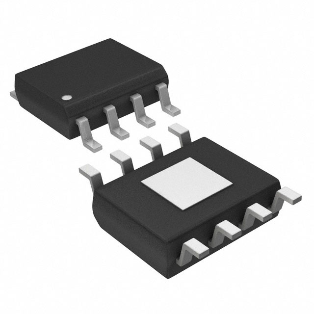
Available in SOIC-8-EDP Lead-free package, fully
WEEE and RoHS compliant
Applications
u
u
u
u
u
u
u
u
The SC4211H is available in the SOIC-8-EDP (Exposed
Die Pad) package. Depending on how the FB pin is configured, the output voltage can be either externally adjusted or fixed to 0.5V.
Typical Application Circuits
Telecom/Networking cards
Motherboards/Peripheral cards
Industrial Applications
Wireless infrastructure
Set top boxes
Medical equipment
Notebook computers
Battery powered systems
SC4211H
4
5
NC
3
VIN
2
ENABLE
NC
VIN
VO
EN
FB
NC
GND
1
6
VO
7
8
R1
VO
=
0.5 (R1 + R2)
Volts
R2
U1
C1
C2
R2
SC4211H
5
4
3
VIN
2
ENABLE
NC
NC
VIN
VO
6
EN
FB
NC
GND
1
VO = 0.5V
7
8
U1
C1
Rev. 2.1
C2
1
www.semtech.com
�SC4211H
POWER MANAGEMENT
Absolute Maximum Ratings
Exceeding the specifications below may result in permanent damage to the device, or device malfunction. Operation outside of the parameters specified in
the Electrical Characteristics section is not implied.
Parameter
Symbol
Max
Units
7
V
PD
Internally Limited
W
θJA
36
°C/W
θJC
5.5
°C/W
Operating Ambient Temperature Range
TA
-40 to +85
°C
Operating Junction Temperature Range
TJ
-40 to +125
°C
TSTG
-65 to +150
°C
TP
260
°C
V ESD
2
kV
Vin, EN, Vo, FB to GND
Power Dissipation
Thermal Resistance Junction to Ambient
Thermal Resistance Junction to Case
(1)
(1)
Storage Temperature Range
Peak IR Reflow Temperature (10s to 30s)
ESD Rating (Human Body Model) (2)
Notes:
(1) Calculated from package in still air, mounted to 3” x 4.5”, 4 layer FR4 PCB with thermal vias under the exposed pad per
JESD51 standards,
(2) Tested according to JEDEC standard JESD22-A114-B.
Electrical Characteristics
Unless specified: VEN = VIN, VFB = VO, VIN = 1.40V to 6.0V, IO = 8mA to 1A.
Values in bold apply over the full operating temperature range.
Parameter
Symbol
Test Conditions
Min
Typ
Max
Units
6.0
V
3
mA
VIN
Supply Voltage Range
VIN
Quiescent Current
IQ
1.40
VIN = 3.3V, IO = 0A
VIN = 6.0V, VEN = 0V
10
50
µA
VO
Line Regulation(1)
REG(LINE)
IO = 10mA
0.2
0.4
%/V
Load Regulation(1)
REG(LOAD)
IO = 10mA to 1A
0.5
1.5
%
VDO
IO = 500mA
100
250
mV
Dropout Voltage(1)(2)
300
2013 Semtech Corp.
2
www.semtech.com
�SC4211H
POWER MANAGEMENT
Electrical Characteristics (Cont.)
Unless specified: VEN = VIN, VFB = VO, VIN = 1.40V to 6.0V, IO = 8mA to 1A.
Values in bold apply over the full operating temperature range.
Parameter
Symbol
Test Conditions
VDO
IO = 1A
Minimum Load Current(3)
IO
VIN = VO + 0.5V
Current Limit(4)
ICL
Min
Typ
Max
200
400
Units
VO (Cont.)
Dropout Voltage(1)(2)
mV
500
8
mA
1.1
1.5
2.0
A
VIN = 3.3V, VFB = VOUT, IO = 10mA
0.495
0.5
0.505
V
Full IOUT , and VIN Range
0.490
F eed b ack
Reference Voltage(1)
Feedback Pin Current(4)
VREF
0.510
IADJ
VFB = VREF
80
200
nA
Enable Pin Current
IEN
VEN = 0V, VIN = 3.3V
1.5
10
µA
Enable Pin Threshold
VIH
VIN = 3.3V
VIL
VIN = 3.3V
EN
1.6
V
0.4
Over Temperature Protection
High Trip level
Hysteresis
Notes:
(1)
(2)
(3)
(4)
THI
160
°C
THYST
10
°C
Low duty cycle pulse testing with Kelvin connections required.
VDO = VIN -VO when VO decreases by 1.5% of its nominal output voltage with VIN = VO +0.8V.
Required to maintain regulation. Voltage set resistors R1 and R2 are usually utilized to meet this requirement.
Guaranteed by design.
2013 Semtech Corp.
3
www.semtech.com
�SC4211H
POWER MANAGEMENT
Ordering Information
Part Number
P ackag e
Temp. Range (TJ)
SC4211HSTRT(1)(2)
SOIC-8-EDP
-40 to +125 OC
SC4211HEVB
Evaluation Board
Notes:
(1) Only available in tape and reel packaging. A reel contains 2500 devices.
(2) Lead-free product. This product is fully WEEE and RoHS
compliant.
Pin Configuration
Pin Descriptions
Pin #
Pin Name
Pin Description
2
EN
Enable Input. Pulling this pin below 0.4V turns the regulator off, reducing the quiescent current to a
fraction of its operating value. The device will be enabled if this pin is left open. Connect to VIN if not
being used.
3
VIN
Input voltage. For regulation at full load, the input to this pin must be between (VO + 0.5V) and 5.5V.
Minimum VIN=1.4V. A large bulk capacitance should be placed closely to this pin to ensure that the
input supply does not sag below 1.4V. Also a minimum of 4.7uF ceramic capacitor should be placed
directly at this pin.
6
VO
The pin is the power output of the device. A minimum of 10uF capacitor should be placed directly at this
pin.
7
FB
Output voltage feedback pin. If connected to the VO pin, the output voltage will be set at 0.5V. If external
feedback resistors are used, the output voltage will be (See Application Circuits on page 1):
VO = [0.5 (R1+R2)] / R2 Volts
8
GND
Reference ground. The GND pin and the exposed die pad must be connected together at the IC pin.
1, 4, 5
NC
No connection.
THERMAL PAD
Pad for heatsinking purposes. Connect to ground plane using multiple vias. Not electrically connected
internally.
2013 Semtech Corp.
4
www.semtech.com
�SC4211H
POWER MANAGEMENT
Block Diagram
Marking Information
Top View
SC4211H
yyww
xxxxx
yyww = Datecode (Example: 0015)
xxxxx = Semtech Lot No. (Example: 00101)
2013 Semtech Corp.
5
www.semtech.com
�SC4211H
POWER MANAGEMENT
Typical Characteristics
Region of Instability
Stable Region
Region of Instability
Region of Instability
Stable Region
Region of Instability
2013 Semtech Corp.
6
www.semtech.com
�SC4211H
POWER MANAGEMENT
Applications Information
Introduction
operating value. A pull up resistor up to 400kOhms should
be connected from this pin to the VIN pin in application
where supply voltages of Vin < 1.9V is required. For applications with higher voltages than 1.9V, EN pin could
be left open or connected to VIN.
The SC4211H is intended for applications where high
current capability and very low dropout voltage are required. It provides a very simple, low cost solution that
uses very little PCB real estate. Additional features include an enable pin to allow for a very low power consumption standby mode, and a fully adjustable output.
Thermal Considerations
The power dissipation in the SC4211H is approximately
equal to the product of the output current and the input
to output voltage differential:
Component Selection
Input capacitor: A large bulk capacitance of about
≥ 10uF/A (output load) should be closely placed to the
input supply pin of the SC4211H to ensure that Vin does
not sag below 1.4V. Also a minimum of 4.7µF ceramic
capacitor is recommended to be placed directly next to
the Vin pin. This allows for the device being some distance from any bulk capacitance on the rail. Additionally,
input droop due to load transients is reduced, improving
load transient response. Additional capacitance may be
added if required by the application.
PD ≈ (VIN − VOUT
)• I O
The absolute worst-case dissipation is given by:
PD(MAX) = (VIN
(MAX)
− VOUT
(MIN)
)• I
O(MAX)
+ VIN
(MAX)
• I Q(MAX)
For a typical scenario, VIN = 3.3V ± 5%, VOUT = 2.8V and
IO = 1A, therefore:
VIN(MAX) = 3.465V, VOUT(MIN) = 2.744V and IQ(MAX) = 1.75mA,
Output capacitor: A minimum bulk capacitance of
≥ 10µF/A (output load), along with a 0.1µF ceramic decoupling capacitor is recommended. Increasing the bulk
capacitance will improve the overall transient response.
The use of multiple lower value ceramic capacitors in
parallel to achieve the desired bulk capacitance will not
cause stability issues. Although designed for use with ceramic output capacitors, the SC4211H is extremely tolerant of output capacitor ESR values and thus will also
work comfortably with tantalum output capacitors.
Thus PD(MAX) = .722W.
Using this figure, and assuming TA(MAX) = 70°C, we can calculate the maximum thermal impedance allowable to maintain TJ ≤ 150°C:
R TH(J −A)(MAX) =
Noise immunity: In very electrically noisy environments,
it is recommended that 0.1µF ceramic capacitors be
placed from IN to GND and OUT to GND as close to the
device pins as possible.
(T
J(MAX)
− TA(MAX) )
PD(MAX)
=
(150 − 70) = 110°C/W
.722
This should be achievable for the SOIC-8-EDP package
using PCB copper area to aid in conducting the heat away,
such as one square inch of copper connected to the ground
pins of the device. Internal ground/power planes and air
flow will also assist in removing heat. For higher ambient
temperatures it may be necessary to use additional copper area.
Internal voltage selection: By connecting the FB pin directly to the VO pin, the output voltage will be regulated
to the 0.5V internal reference.
External voltage selection resistors: The use of 1%
resistors, and designing for a current flow ≥ 8mA is
recommended to ensure a well regulated output (thus
R2 ≤ 62.5Ω).
Enable: Pulling this pin below 0.4V turns the regulator
off, reducing the quiescent current to a fraction of its
2013 Semtech Corp.
7
www.semtech.com
�SC4211H
POWER MANAGEMENT
Outline Drawing - SOIC-8-EDP
A
D
e
DIMENSIONS
MILLIMETERS
DIM
MIN NOM MAX
N
E1 E
1
2
ccc C
2X N/2 TIPS
e/2
B
D
aaa C
A2 A
SEATING
PLANE
C
1.35
1.75
0.13
0.00
1.25
1.65
0.31
0.51
0.17
0.25
4.80 4.90 5.00
3.80 3.90 4.00
6.00 BSC
1.27 BSC
2.95
3.50
2.15
2.60
0.25
0.50
0.40 0.72 1.04
(1.05)
8
0°
8°
0.10
0.25
0.20
A
A1
A2
b
c
D
E1
E
e
F
H
h
L
L1
N
01
aaa
bbb
ccc
E/2
A1
bxN
bbb
C A-B D
h
F
h
EXPOSED PAD
H
H
c
GAUGE
PLANE
L
(L1)
0.25
DETAIL
SEE DETAIL
01
A
A
SIDE VIEW
NOTES:
1.
CONTROLLING DIMENSIONS ARE IN MILLIMETERS (ANGLES IN DEGREES).
2. DATUMS -A- AND -B- TO BE DETERMINED AT DATUM PLANE -H- .
3. DIMENSIONS "E1" AND "D" DO NOT INCLUDE MOLD FLASH, PROTRUSIONS OR GATE BURRS.
4. THE MEASUREMENT OF DIMENSION "F" DOES NOT INCLUDE EXPOSED TIE BAR.
2013 Semtech Corp.
8
www.semtech.com
�SC4211H
POWER MANAGEMENT
Land Pattern - SOIC-8-EDP
E
SOLDER
MASK
D
(C)
F
G
Z
Y
THERMAL VIA
Ø 0.36mm
P
DIMENSIONS
DIM MILLIMETERS
(5.30)
C
D
3.50
E
5.10
F
2.60
3.20
G
P
1.27
X
0.60
Y
2.10
Z
7.40
X
NOTES:
1. CONTROLLING DIMENSIONS ARE IN MILLIMETERS (ANGLES IN DEGREES).
2. THIS LAND PATTERN IS FOR REFERENCE PURPOSE ONLY.
CONSULT YOUR MANUFACTURING GROUP TO ENSURE YOUR
COMPANY'S MANUFACTURING GUIDELINES ARE MET.
3. THERMAL VIAS IN THE LAND PATTERN OF THE EXPOSED PAD SHALL BE
CONNECTED TO A SYSTEM GROUND PLANE. FAILURE TO DO SO MAY
COMPROMISE THE THERMAL AND/OR FUNCTIONAL PERFORMANCE OF
THE DEVICE.
4. REFERENCE IPC-SM-782A, SECTION 9.1, RLP NO. 300A.
Contact Information
Semtech Corporation
Power Management Products Division
200 Flynn Road, Camarillo, CA 93012
Phone: (805)498-2111 FAX (805)498-3804
2013 Semtech Corp.
9
www.semtech.com
��


 工商网监
湘ICP备2023018690号
工商网监
湘ICP备2023018690号
