SX1280/SX1281
Long Range, Low Power, 2.4 GHz
Transceiver with Ranging Capability
Analog Front End & Data Conversion
LORA
Modem
& Ranging
ADC
LNA
Protocol
Engine
FLRC
Modem
Match
PA
SPI or UART
PLL
FSK
Modem
OSC
DC-DC
Data
Buffer
LDO
Figure A: Transceiver Block Diagram
General Description
Key Features
The SX1280/1 transceiver family provides ultra long range
communication in the 2.4 GHz band with the linearity to
withstand heavy interference. This makes them the ideal
solution for robust and reliable wireless solutions. They are
the first ISM band transceiver IC of their kind to integrate a
time-of-flight functionality, opening up application
solutions to track and localize assets in logistic chains and
people for safety. These long range 2.4 GHz products
include multiple physical layers and modulations to
optimize long range communication at high data rate for
video and security applications. Very small products for
wearables can easily be designed thanks to the high level
of integration and the ultra-low current consumption
which allows the use of miniaturized batteries.
The radio is fully compliant with all worldwide 2.4 GHz
radio regulations including EN 300 440, FCC CFR 47 Part 15
and the Japanese ARIB STD-T66.
The level of integration, low consumption and ranging
functions within the long range 2.4 GHz product line
enable enhanced connectivity and provide additional
functionality to a new generation of previously
unconnected devices and applications.
SX1280/SX1281
Data Sheet
DS.SX1280-1.W.APP
• Long Range 2.4 GHz transceiver
• High sensitivity, down to -132 dBm
• +12.5 dBm, high efficiency PA
• Low energy consumption, on-chip DC-DC
• LoRa®, FLRC, (G)FSK supported modulations
• Programmable bit rate
• Excellent blocking immunity
• Standard & Advanced Ranging Engine, Time-of-Flight
• BLE PHY layer compatibility
• Low system cost
Applications
• Home automation & appliances
• IIoT Asset Management and Safety
• Logistics Tracking applications
• Sports /Fitness sensors and smart watches
• Radio-controlled toys & drones
• Agriculture
• Healthcare
www.semtech.com
Rev 3.2
March 2020
1 of 158
Semtech
�Ordering Information
Part Number
Delivery
Order Quantity
SX1280IMLTRT
Tape & Reel
3’000 pieces
SX1281IMLTRT
Tape & Reel
3’000 pieces
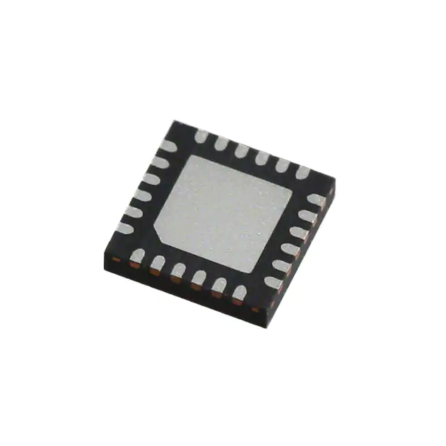
QFN 24 Package, with the temperature operating range from -40 to 85°C
Pb-free, Halogen free, RoHS/WEEE compliant product
Revision History
Version
ECO
Date
Rev 1.0
035543
February 2017
Changes and/or Modifications
First Release
Added table of effective data rates for the LoRa® Modem
Correction of the formulas for time-on-air in LoRa®
Rev 1.1
037029
May 2017
Correction of typos in the chapter Host Controller Interface
Update of the application schematic with optional TCXO
Update of the reference design BOM
Deletion of redundant information in the chapter Thermal Impedance
The maximum SPI clock speed is reduced to 18 MHz
Addition of a note in chapter 6.2.3 "Bandwidth" on SF and BW to be known in advance
Addition of chapter 6.2.6 "Frequency Error"
Addition of calculations of time-on-air in chapter 7.5 "LoRa Ranging Engine Packet"
Rev 2.0
040575
February 2018
Addition of examples of SPI communication in chapter 11 "Host Controller Interface"
Update of explanation on SetAutoTx in chapter 13.2.4 "BLE Specific Functions"
Update of ranging results description in chapter 13.5 "Ranging Operation"
Addition of an explanation of the Reference Design in chapter 14.1 "Reference Design"
Addition of the tape and reel specifications in chapter 15 "Packaging Information"
Addition of LoRa® and Bluetooth® trademark information
Maximum RF input power (ML) is now 0 dBm
Phase noise at 2.45 GHz with 1 MHz offset (PHN) is now -115 dBc/Hz
Correction of minor typographical errors in tables 6-5, 6-7, 13-20 and in chapter 7.2
Rev 2.1
041639
April 2018
Addition of formulas for ranging duration in chapter 7.5.4
Addition of description of RSSI packet for LoRa® when SNR ≤ 0 in table 11-64
Correction of package thickness to 0.9 mm in chapter 15.1
Addition of package marking in chapter 15.2
SX1280/SX1281
Data Sheet
DS.SX1280-1.W.APP
www.semtech.com
Rev 3.2
March 2020
2 of 158
Semtech
�Version
ECO
Date
Changes and/or Modifications (Continued)
The following specifications have been changed:
• The 3rd order input intercept for maximum low power gain setting (IIP3)
- at 6 MHz offset, has been changed from -6 dBm to -12 dBm
- at 10 and 20 MHz offset, has been improved from -6 dBm to 0 dBm
• IDDSTDBYRC has been improved from 760 μA to 700 μA
• IDDSTDBYXOSC has been improved from 1.2 mA to 1 mA
• PHN 10 MHz has been improved from -133 dBc/Hz to -135 dBc/Hz
• TS_OS has been improved from 100 μs to 40 μs
• RFSHS_L , SF7, BW = 1625 kHz, has been changed from -109 dBm to -108 dBm
Rev 2.2
041738
May 2018
The switching times have been modified for the following transitions:
• SLEEP to STDBY_RC from 1700 μs to 1200 μs
• SLEEP to STDBY_RC from 250 μs to 130 μs
• STDBY_RC to STDBY_XOSC from 53 μs to 40 μs
• STDBY_RC to FS from 83 μs to 55 μs
• STDBY_RC to Rx from 115 μs to 85 μs
• STDBY_RC to Tx from 102 μs to 80 μs
• STDBY_XOSC to FS from 40 μs to 54 μs
Table 6-2 now gives the raw data rates when using LoRa®
Formulas of time-on-air for long interleaving in LoRa® mode have been updated in
chapter 7.4.4
SX1282 Added to the product family together with descriptions of its Advanced
Ranging functionality.
Improved description and detail of register retention in the Sleep Mode
description of Section 11.5
FSK Mode enhanced Synch word description and graphics in Section 7 and
Section 11, Tx mode now described in full.
Rev 3.0
047476
July 2019
Internal
Release
Reference to long interleaving removed from ranging section.
Detailed description of SPI bus sharing without false detection as UART
interface.
Correction of maximum FLRC Bandwidth to 1.2 MHz.
Correction of FLRC sensitivity specification to 1.2 MHz value.
SX1280/SX1281
Data Sheet
DS.SX1280-1.W.APP
www.semtech.com
Rev 3.2
March 2020
3 of 158
Semtech
�Version
ECO
Date
Changes and/or Modifications (Continued)
Added table of device registers.
Change of VBAT_IO tolerance down to 1.7 V.
VOL and VOH Specification update with VBAT_IO = 1.7 V.
RTC Calibration process documented.
Description of Ranging RSSI added.
Image frequency added.
FEI Resolution table and description added.
Correction of FLRC time on air formulae.
Rev 3.1
048727
Internal
Release
September
2019
Correction of LoRa time on air formulae.
Performance counter test mode removed.
Correction of coding rate in long interleaving mode.
Typographical corrections.
LoRa modem frequency error tolerance reduced.
UART Speed change functionality documented.
SNR Usage clarified.
BER Specification for FSK Updated
FLRC IRQ modification
Text and typographical corrections.
Integration of SX1282 functionality into SX1280.
Additional registers added to the register map.
Rev 3.2
051322
March
2020
TCXO Output voltage added.
FLRC CRC length correction.
Description on high traffic, continuous mode issue.
Description of FLRC elevated PER for certain Synch Word settings.
SX1280/SX1281
Data Sheet
DS.SX1280-1.W.APP
www.semtech.com
Rev 3.2
March 2020
4 of 158
Semtech
�Table of Contents
General Description.............................................................................................................................................1
Key Features...........................................................................................................................................................1
Applications ...........................................................................................................................................................1
Ordering Information .........................................................................................................................................2
Revision History ....................................................................................................................................................2
List of Figures ..................................................................................................................................................... 10
List of Tables ...................................................................................................................................................... 11
1. Introduction.................................................................................................................................................... 15
1.1 Analog Front End ............................................................................................................................. 15
1.2 Power Distribution .......................................................................................................................... 15
1.3 Modem ................................................................................................................................................ 15
1.4 Packet Processing ............................................................................................................................ 16
1.5 Digital Interface and Control ....................................................................................................... 16
2. Pin Connections ............................................................................................................................................ 17
2.1 Transceiver Pinout ........................................................................................................................... 17
2.2 Package view ..................................................................................................................................... 18
3. Specifications ................................................................................................................................................. 19
3.1 ESD Notice .......................................................................................................................................... 19
3.2 Absolute Minimum and Maximum Ratings ........................................................................... 19
3.3 Operating Range .............................................................................................................................. 19
3.4 General Electrical Specifications ................................................................................................ 20
3.5 Receiver Electrical Specifications ............................................................................................... 21
3.5.1 Receiver Specifications...................................................................................................... 21
3.5.2 LoRa® Modem ...................................................................................................................... 22
3.5.3 FLRC Modem......................................................................................................................... 24
3.5.4 FSK Modem............................................................................................................................ 25
3.6 Transmitter Electrical Specifications ......................................................................................... 26
3.7 Crystal Oscillator Specifications ................................................................................................. 26
3.8 Digital Pin Levels .............................................................................................................................. 27
4. Analog Front End.......................................................................................................................................... 28
4.1 Transmitter ......................................................................................................................................... 28
4.2 Receiver ............................................................................................................................................... 29
4.2.1 Low Power Mode and High Sensitivity Mode........................................................... 30
4.2.2 Image Frequency................................................................................................................. 30
4.2.3 Wi-Fi and Bluetooth Immunity ....................................................................................... 30
4.3 PLL ......................................................................................................................................................... 30
4.4 RC Oscillators .................................................................................................................................... 31
5. Power Distribution ....................................................................................................................................... 32
5.1 Selecting DC-DC Converter or LDO Regulation ................................................................... 32
5.2 Flexible DIO Supply ........................................................................................................................ 33
6. Digital Baseband........................................................................................................................................... 34
6.1 Overview ............................................................................................................................................. 34
6.2 LoRa® Modem ................................................................................................................................... 35
SX1280/SX1281
Data Sheet
DS.SX1280-1.W.APP
www.semtech.com
Rev 3.2
March 2020
5 of 158
Semtech
�6.2.1 LoRa® Modulation ............................................................................................................... 35
6.2.2 Spreading Factor ................................................................................................................. 35
6.2.3 Bandwidth.............................................................................................................................. 36
6.2.4 Forward Error Correction Coding Rate ........................................................................ 36
6.2.5 Ranging Engine.................................................................................................................... 37
6.2.6 Advanced Ranging ............................................................................................................. 37
6.2.7 Frequency Error.................................................................................................................... 37
6.3 FLRC Modem ..................................................................................................................................... 38
6.3.1 Modem Bandwidth and Data Rates.............................................................................. 38
6.3.2 FEC Coding Rate .................................................................................................................. 39
6.3.3 Gaussian Filtering................................................................................................................ 40
6.4 FSK Modem ........................................................................................................................................ 41
6.4.1 Modem Bandwidth and Data Rates.............................................................................. 41
6.4.2 Modem Modulation Index ............................................................................................... 42
6.5 Guidance on Modem Selection .................................................................................................. 43
7. Packet Engine................................................................................................................................................. 44
7.1 GFSK Packet ....................................................................................................................................... 45
7.1.1 Fixed-length Packet Format ............................................................................................ 45
7.1.2 Variable-length Packet Format....................................................................................... 45
7.2 BLE Packet Format ........................................................................................................................... 46
7.3 FLRC Packet ....................................................................................................................................... 47
7.3.1 FLRC Packet Format............................................................................................................ 47
7.3.2 Fixed-Length Packet Format ........................................................................................... 47
7.3.3 Variable-length Packet Format....................................................................................... 48
7.3.4 FLRC Time-on-Air................................................................................................................. 48
7.4 LoRa® Packet ...................................................................................................................................... 49
7.4.1 LoRa® Packet Format.......................................................................................................... 49
7.4.2 Explicit (Variable-length) Header Mode...................................................................... 49
7.4.3 Implicit (Fixed-length) Header Mode........................................................................... 50
7.4.4 LoRa® Time-on-Air............................................................................................................... 50
7.5 LoRa® Ranging Engine Packet ..................................................................................................... 53
7.5.1 Ranging Packet Format..................................................................................................... 53
7.5.2 Ranging Master Exchange ............................................................................................... 54
7.5.3 Ranging Slave Exchange................................................................................................... 54
7.5.4 Total Exchange Duration .................................................................................................. 55
7.5.5 Measurement........................................................................................................................ 56
8. Data Buffer ...................................................................................................................................................... 57
8.1 Principle of Operation .................................................................................................................... 57
8.2 Receive Operation ........................................................................................................................... 58
8.3 Transmit Operation ......................................................................................................................... 58
8.4 Using the Data buffer ..................................................................................................................... 58
9. Digital Interface and Control .................................................................................................................... 59
9.1 BUSY Pin Communication ............................................................................................................ 59
9.2 Interface Detection ......................................................................................................................... 59
9.3 SPI Interface ....................................................................................................................................... 60
9.3.1 SPI Timing .............................................................................................................................. 60
SX1280/SX1281
Data Sheet
DS.SX1280-1.W.APP
www.semtech.com
Rev 3.2
March 2020
6 of 158
Semtech
�9.3.2 SPI Timing When the Transceiver is in Active Mode............................................... 61
9.3.3 SPI Timing When the Transceiver Leaves Sleep Mode .......................................... 62
9.4 UART Interface .................................................................................................................................. 64
9.4.1 Default UART Settings ....................................................................................................... 64
9.4.2 Setting the UART Speed.................................................................................................... 64
9.5 Pin Sharing ......................................................................................................................................... 64
9.6 Multi-Purpose Digital Input/Output (DIO) ............................................................................. 64
9.7 Transceiver Initialization on a Shared SPI Bus ....................................................................... 65
10. Operational Modes.................................................................................................................................... 67
10.1 Startup .............................................................................................................................................. 67
10.2 Sleep Mode ..................................................................................................................................... 67
10.3 Standby Mode ................................................................................................................................ 68
10.4 Frequency Synthesis (FS) Mode ............................................................................................... 68
10.5 Receive (Rx) Mode ......................................................................................................................... 68
10.6 Transmit (Tx) Mode ....................................................................................................................... 68
10.7 Transceiver Circuit Modes Graphical Illustration ............................................................... 69
10.8 Active Mode Switching Time .................................................................................................... 70
11. Host Controller Interface ......................................................................................................................... 71
11.1 Command Structure .................................................................................................................... 71
11.2 SetUartSpeed Command ........................................................................................................... 72
11.3 GetStatus Command ................................................................................................................... 72
11.4 Register Access Operations ....................................................................................................... 74
11.4.1 WriteRegister Command................................................................................................ 74
11.4.2 ReadRegister Command ................................................................................................ 75
11.5 Data Buffer Operations ............................................................................................................... 75
11.5.1 WriteBuffer Command .................................................................................................... 75
11.5.2 ReadBuffer........................................................................................................................... 76
11.6 Radio Operation Modes .............................................................................................................. 77
11.6.1 SetSleep................................................................................................................................ 77
11.6.2 SetStandby .......................................................................................................................... 78
11.6.3 SetFs....................................................................................................................................... 78
11.6.4 SetTx ...................................................................................................................................... 79
11.6.5 SetRx...................................................................................................................................... 80
11.6.6 SetRxDutyCycle ................................................................................................................. 81
11.6.7 SetLongPreamble ............................................................................................................. 82
11.6.8 SetCAD.................................................................................................................................. 83
11.6.9 SetTxContinuousWave.................................................................................................... 83
11.6.10 SetTxContinuousPreamble ......................................................................................... 83
11.6.11 SetAutoTx.......................................................................................................................... 84
11.6.12 SetAutoFs .......................................................................................................................... 85
11.7 Radio Configuration ..................................................................................................................... 85
11.7.1 SetPacketType.................................................................................................................... 85
11.7.2 GetPacketType................................................................................................................... 86
11.7.3 SetRfFrequency.................................................................................................................. 87
11.7.4 SetTxParams ....................................................................................................................... 87
11.7.5 SetCadParams .................................................................................................................... 88
SX1280/SX1281
Data Sheet
DS.SX1280-1.W.APP
www.semtech.com
Rev 3.2
March 2020
7 of 158
Semtech
�11.7.6 SetBufferBaseAddress ..................................................................................................... 89
11.7.7 SetModulationParams..................................................................................................... 89
11.7.8 SetPacketParams............................................................................................................... 90
11.8 Communication Status Information ...................................................................................... 92
11.8.1 GetRxBufferStatus............................................................................................................. 92
11.8.2 GetPacketStatus ................................................................................................................ 93
11.8.3 GetRssiInst ........................................................................................................................... 95
11.9 IRQ Handling ................................................................................................................................... 95
11.9.1 SetDioIrqParams................................................................................................................ 96
11.9.2 GetIrqStatus ........................................................................................................................ 97
11.9.3 ClearIrqStatus ..................................................................................................................... 97
12. List of Commands ...................................................................................................................................... 99
13. Register Map .............................................................................................................................................101
14. Transceiver Operation ............................................................................................................................104
14.1 GFSK Operation ...........................................................................................................................104
14.1.1 Common Transceiver Settings...................................................................................104
14.1.2 Tx Setting and Operations...........................................................................................110
14.1.3 Rx Setting and Operations...........................................................................................111
14.2 BLE Operation ...............................................................................................................................113
14.2.1 Common Transceiver Settings...................................................................................113
14.2.2 Tx Setting and Operations...........................................................................................116
14.2.3 Rx Setting and Operations...........................................................................................117
14.2.4 BLE Specific Functions ..................................................................................................119
14.3 FLRC Operation ............................................................................................................................121
14.3.1 Common Transceiver Settings...................................................................................121
14.3.2 Tx Setting and Operations...........................................................................................126
14.3.3 Rx Setting and Operations...........................................................................................127
14.4 LoRa® Operation ..........................................................................................................................130
14.4.1 Common Transceiver Settings for LoRa® ...............................................................130
14.4.2 Tx Setting and Operations...........................................................................................133
14.4.3 Rx Setting and Operations...........................................................................................134
14.5 Ranging Operation .....................................................................................................................136
14.5.1 Ranging Device Setting ................................................................................................136
14.5.2 Ranging Operation as State Machines ....................................................................140
14.5.3 Ranging RSSI.....................................................................................................................141
14.6 Advanced Ranging .....................................................................................................................142
14.6.1 Advanced Ranging Mode Operation.......................................................................142
14.6.2 Advanced Ranging State Machine .........................................................................143
14.7 Miscellaneous Functions ..........................................................................................................143
14.7.1 SetRegulatorMode Command ...................................................................................143
14.7.2 Context Saving.................................................................................................................144
15. Reference Design and Application Schematics ............................................................................145
15.1 Reference Design ........................................................................................................................145
15.1.1 Application Design Schematic...................................................................................145
15.1.2 Reference Design BOM .................................................................................................146
15.1.3 Reference Design PCB...................................................................................................146
SX1280/SX1281
Data Sheet
DS.SX1280-1.W.APP
www.semtech.com
Rev 3.2
March 2020
8 of 158
Semtech
�15.2 Application Design with optional TCXO .............................................................................147
15.3 Application Design with Low Drop Out Regulator .........................................................147
15.4 Sleep Mode Consumption .......................................................................................................148
16. Errata.............................................................................................................................................................149
16.1 All Modems: Continuous Receive Mode in Congested Traffic ................................... 149
16.1.1 Problem Description......................................................................................................149
16.1.2 Problem Solution ............................................................................................................149
16.2 LoRa Modem: Additional Header Checks Required .......................................................150
16.2.1 Problem Description......................................................................................................150
16.2.2 Problem Solution ............................................................................................................150
16.3 All Modems: Interrupt with Bad CRC ...................................................................................150
16.3.1 Problem Description......................................................................................................150
16.3.2 Problem Solution ............................................................................................................150
16.4 FLRC Modem: Increased PER in FLRC Packets with Synch Word ...............................151
16.4.1 Problem Description......................................................................................................151
16.4.2 Problem Solution ............................................................................................................151
17. Packaging Information...........................................................................................................................152
17.1 Package Outline Drawing ........................................................................................................152
17.2 Package Marking .........................................................................................................................153
17.3 Land Pattern .................................................................................................................................153
17.4 Reflow Profiles ..............................................................................................................................154
17.5 Thermal Impedance ...................................................................................................................154
17.6 Tape and Reel Specification ....................................................................................................154
Glossary ..............................................................................................................................................................155
SX1280/SX1281
Data Sheet
DS.SX1280-1.W.APP
www.semtech.com
Rev 3.2
March 2020
9 of 158
Semtech
�List of Figures
Figure 2-1: Transceiver Pin Locations ....................................................................................................... 18
Figure 4-1: Transceiver Block Diagram, Analog Front End Highlighted....................................... 28
Figure 5-1: Transceiver Block Diagram, Power Distribution Highlighted .................................... 32
Figure 5-2: Separate DIO Supply................................................................................................................. 33
Figure 6-1: Transceiver Block Diagram, Modems Highlighted ........................................................ 34
Figure 6-2: FSK Modulation Parameters................................................................................................... 41
Figure 6-3: Sensitivity Performance of the Transceiver Modems ................................................... 43
Figure 7-1: Transceiver Block Diagram, Packet Engine Highlighted.............................................. 44
Figure 7-2: Fixed-length Packet Format................................................................................................... 45
Figure 7-3: Variable-length Packet Format ............................................................................................. 45
Figure 7-4: BLE Packet Format..................................................................................................................... 46
Figure 7-5: PDU Header Format .................................................................................................................. 46
Figure 7-6: FLRC Fixed-length Packet Format........................................................................................ 47
Figure 7-7: FLRC Variable-length Packet Format .................................................................................. 48
Figure 7-8: LoRa® Variable-length Packet Format ................................................................................ 49
Figure 7-9: LoRa® Fixed-length Packet Format...................................................................................... 50
Figure 7-10: Ranging Packet Format......................................................................................................... 53
Figure 7-11: Ranging Master Packet Exchange ..................................................................................... 54
Figure 7-12: Ranging Slave Packet Exchange ........................................................................................ 54
Figure 7-13: Ranging Measurement.......................................................................................................... 56
Figure 8-1: Data Buffer Diagram ................................................................................................................. 57
Figure 9-1: Transceiver Block Diagram, Digital Interface Highlighted.......................................... 59
Figure 9-2: SPI Timing Diagram................................................................................................................... 61
Figure 9-3: SPI Wake-UpTiming Transition ............................................................................................. 62
Figure 9-4: SPI NSS Pulse Timing Transition ........................................................................................... 63
Figure 9-5: Multiple Radios Sharing an SPI Bus With a Sensor......................................................... 66
Figure 10-1: Transceiver Circuit Modes .................................................................................................... 69
Figure 10-2: Switching Time Definition in Active Mode .................................................................... 70
Figure 14-1: Ranging Application State Machine Diagram............................................................. 140
Figure 14-2: Example Ranging RSSI Response (may vary depending upon SF BW used) ... 141
Figure 14-3: ...................................................................................................................................................... 143
Figure 14-4: Advanced Ranging Mode State Machine ..................................................................... 143
Figure 15-1: Transceiver Application Design Schematic ................................................................. 145
Figure 15-2: Long Range Reference Design PCB Layout.................................................................. 146
Figure 15-3: Application Schematic with Optional TCXO................................................................ 147
Figure 15-4: Application Schematic with Low Drop Out Regulator Schematic ...................... 147
Figure 17-1: QFN 4x4 Package Outline Drawing................................................................................. 152
Figure 17-2: SX1280 and SX1281 Package Marking .......................................................................... 153
Figure 17-3: QFN 4x4mm Land Pattern.................................................................................................. 153
Figure 17-4: Tape and Reel Specification .............................................................................................. 154
SX1280/SX1281
Data Sheet
DS.SX1280-1.W.APP
www.semtech.com
Rev 3.2
March 2020
10 of 158
Semtech
�List of Tables
Table 1-1: Product Portfolio and Modem Functionality.....................................................................
Table 2-1: Transceiver Pinout.......................................................................................................................
Table 3-1: Minimum and Maximum Ratings ..........................................................................................
Table 3-2: Operating Range..........................................................................................................................
Table 3-3: General Electrical Specifications ............................................................................................
Table 3-4: Receiver Specifications ..............................................................................................................
Table 3-5: LoRa® Modem Specifications ..................................................................................................
Table 3-6: FLRC Modem Specifications ....................................................................................................
Table 3-7: FSK Modem Specifications .......................................................................................................
Table 3-8: Transmitter Electrical Specifications.....................................................................................
Table 3-9: Crystal Oscillator Specifications .............................................................................................
Table 3-10: Digital Levels and Timings.....................................................................................................
Table 4-1: Procedure for Receiver Gain Manual Setting.....................................................................
Table 4-2: Receiver Gain Manual Setting .................................................................................................
Table 5-1: Regulation Type versus Circuit Mode...................................................................................
Table 6-1: Receiver Sensitivity when using LoRa® in Low Power Mode .......................................
Table 6-2: Raw Data Rates when using LoRa®........................................................................................
Table 6-3: Total Permissible Reference Drift...........................................................................................
Table 6-4: Valid FLRC Data Rate and Bandwidth Combinations ....................................................
Table 6-5: Effective FLRC Data Rates Based upon FEC Usage with Resulting Sensitivities....
Table 6-6: Receiver Performance of the FLRC Modem .......................................................................
Table 6-7: Valid FSK Data Rate and Bandwidth Combinations with Resulting Sensitivities .
Table 9-1: SPI Timing Requirements..........................................................................................................
Table 10-1: SX1280 Operating Modes ......................................................................................................
Table 10-2: Switching Time (TswMode) for all Possible Transitions ..............................................
Table 11-1: SPI interface Command Sequence .....................................................................................
Table 11-2: UART Interface Command Sequence ................................................................................
Table 11-3: SetUartSpeed Data Transfer (UART only) .........................................................................
Table 11-4: Divider Ratios to Configure the UART Interface Speed ...............................................
Table 11-5: Status Byte Definition..............................................................................................................
Table 11-6: GetStatus Data Transfer (SPI) ................................................................................................
Table 11-7: GetStatus Data Transfer (UART) ...........................................................................................
Table 11-8: WriteRegister Data Transfer (SPI).........................................................................................
Table 11-9: WriteRegister Data Transfer (UART)....................................................................................
Table 11-10: ReadRegister Data Transfer (SPI).......................................................................................
Table 11-11: ReadRegister Data Transfer (UART)..................................................................................
Table 11-12: WriteBuffer SPI Data Transfer .............................................................................................
Table 11-13: WriteBuffer UART Data Transfer ........................................................................................
Table 11-14: ReadBuffer SPI Data Transfer..............................................................................................
Table 11-15: ReadBuffer UART Data Transfer.........................................................................................
Table 11-16: SetSleep SPI Data Transfer...................................................................................................
Table 11-17: Sleep Mode Definition ..........................................................................................................
Table 11-18: SetStandby SPI Data Transfer.............................................................................................
Table 11-19: SetStandby UART Data Transfer........................................................................................
Table 11-20: StandbyConfig Definition....................................................................................................
Table 11-21: SetFs Data Transfer ................................................................................................................
Table 11-22: SetTx SPI Data Transfer .........................................................................................................
Table 11-23: SetTx UART Data Transfer ....................................................................................................
Table 11-24: SetTx Time-out Definition. ..................................................................................................
Table 11-25: SetTx Time-out Duration......................................................................................................
SX1280/SX1281
Data Sheet
DS.SX1280-1.W.APP
www.semtech.com
Rev 3.2
March 2020
15
17
19
19
20
21
22
24
25
26
26
27
29
29
32
35
36
37
38
39
40
42
60
67
70
71
71
72
72
73
73
73
74
74
75
75
75
76
76
76
77
77
78
78
78
79
79
79
79
80
11 of 158
Semtech
�Table 11-26: SetRx SPI Data Transfer.........................................................................................................
Table 11-27: SetRx UART Data Transfer....................................................................................................
Table 11-28: SetRx Time-out Duration .....................................................................................................
Table 11-29: Duty Cycled Operation SPI Data Transfer ......................................................................
Table 11-30: Duty Cycled Operation UART Data Transfer .................................................................
Table 11-31: Rx Duration Definition. .........................................................................................................
Table 11-32: SetLongPreamble Data Transfer .......................................................................................
Table 11-33: SetCAD Data Transfer............................................................................................................
Table 11-34: SetTxContinuousWave Data Transfer..............................................................................
Table 11-35: SetTxContinuousPreamble Data Transfer .....................................................................
Table 11-36: SetAutoTx SPI Data Transfer ...............................................................................................
Table 11-37: SetAutoTx UART Data Transfer ..........................................................................................
Table 11-38: SetAutoFs SPI Data Transfer ...............................................................................................
Table 11-39: SetAutoFs UART Data Transfer...........................................................................................
Table 11-40: SetPacketType SPI Data Transfer ......................................................................................
Table 11-41: SetPacketType UART Data Transfer .................................................................................
Table 11-42: PacketType Definition...........................................................................................................
Table 11-43: GetPacketType SPI Data Transfer......................................................................................
Table 11-45: SetRfFrequency SPI Data Transfer ....................................................................................
Table 11-46: SetRfFrequency UART Data Transfer ...............................................................................
Table 11-47: SetTxParams SPI Data Transfer ..........................................................................................
Table 11-44: GetPacketType UART Data Transfer.................................................................................
Table 11-49: RampTime Definition ............................................................................................................
Table 11-50: CAD SPI Data Transfer ...........................................................................................................
Table 11-51: CAD UART Data Transfer ......................................................................................................
Table 11-48: SetTxParams UART Data Transfer .....................................................................................
Table 11-52: CadSymbolNum Definition.................................................................................................
Table 11-53: SetBufferBaseAddress SPI Data Transfer ........................................................................
Table 11-54: SetBufferBaseAddress UART Data Transfer ...................................................................
Table 11-55: SetModulationParams SPI Data Transfer .......................................................................
Table 11-57: SetModulationParams Parameters Definition..............................................................
Table 11-58: SetPacketParams SPI Data Transfer..................................................................................
Table 11-56: SetModulationParams UART Data Transfer ..................................................................
Table 11-60: SetPacketParams Parameters Definition........................................................................
Table 11-59: SetPacketParams UART Data Transfer.............................................................................
Table 11-61: GetRxBufferStatus SPI Data Transfer ...............................................................................
Table 11-62: GetRxBufferStatus UART Data Transfer ..........................................................................
Table 11-63: GetPacketStatus SPI Data Transfer ...................................................................................
Table 11-64: GetPacketStatus UART Data Transfer ..............................................................................
Table 11-65: packetStatus Definition........................................................................................................
Table 11-66: RSSI and SNR Packet Status.................................................................................................
Table 11-67: Status Packet Status Byte.....................................................................................................
Table 11-68: Error Packet Status Byte .......................................................................................................
Table 11-69: Sync Packet Status Byte........................................................................................................
Table 11-70: GetRssiInst SPI Data Transfer..............................................................................................
Table 11-71: GetRssiInst UART Data Transfer .........................................................................................
Table 11-72: RssiInst Definition ...................................................................................................................
Table 11-73: IRQ Register...............................................................................................................................
Table 11-74: IRQ Mask Definition SPI Data Transfer ............................................................................
Table 11-75: IRQ Mask Definition UART Data Transfer .......................................................................
Table 11-76: GetIrqStatus SPI Data Transfer...........................................................................................
Table 11-77: GetIrqStatus UART Data Transfer......................................................................................
Table 11-78: ClearIrqStatus SPI Data Transfer........................................................................................
Table 11-79: ClearIrqStatus UART Data Transfer...................................................................................
SX1280/SX1281
Data Sheet
DS.SX1280-1.W.APP
www.semtech.com
Rev 3.2
March 2020
80
80
81
81
81
82
83
83
83
84
84
84
85
85
86
86
86
86
87
87
87
87
88
88
88
88
89
89
89
89
90
90
90
91
91
92
92
93
93
93
93
94
94
94
95
95
95
95
96
96
97
97
97
97
12 of 158
Semtech
�Table 12-1: Transceiver Available Commands....................................................................................... 99
Table 13-1: List of Registers ........................................................................................................................ 101
Table 14-1: Modulation Parameters in GFSK Mode ........................................................................... 104
Table 14-2: Modulation Index Parameters in GFSK Mode............................................................... 105
Table 14-3: Modulation Shaping Parameters in GFSK Mode.......................................................... 106
Table 14-4: Preamble Length Definition in GFSK Packet ................................................................. 106
Table 14-5: Sync Word Length Definition in GFSK Packet............................................................... 107
Table 14-6: Sync Word Combination in GFSK Packet........................................................................ 107
Table 14-7: Packet Type Definition in GFSK Packet ........................................................................... 107
Table 14-8: Payload Length Definition in GFSK Packet .................................................................... 108
Table 14-9: CRC Definition in GFSK Packet ........................................................................................... 108
Table 14-10: Whitening Enabling in GFSK Packet .............................................................................. 108
Table 14-11: Sync Word Definition in GFSK Packet............................................................................ 108
Table 14-12: CRC Initialization Registers................................................................................................ 109
Table 14-13: CRC Polynomial Definition ................................................................................................ 109
Table 14-14: PacketStatus[3] in GFSK Packet ....................................................................................... 110
Table 14-15: PacketStatus[2] in GFSK Packet ....................................................................................... 112
Table 14-16: PacketStatus[4] in GFSK Mode Packet........................................................................... 112
Table 14-17: Modulation Parameters in BLE and GFSK Mode........................................................ 113
Table 14-18: Modulation Parameters in BLE and GFSK Mode........................................................ 114
Table 14-19: Modulation Parameters in BLE and GFSK Mode........................................................ 114
Table 14-20: Connection State Definition in BLE Packet.................................................................. 114
Table 14-21: CRC Definition in BLE Packet ............................................................................................ 114
Table 14-22: Tx Test Packet Payload in Test Mode for BLE Packet ............................................... 115
Table 14-23: Whitening Enabling in BLE Packet.................................................................................. 115
Table 14-24: Access Address Definition in BLE Packet...................................................................... 116
Table 14-25: CRC Initialization Registers................................................................................................ 116
Table 14-26: BLE Access Address Configuration for Tx..................................................................... 116
Table 14-27: PacketStatus3 in BLE Packet ............................................................................................. 117
Table 14-28: PacketStatus2 in BLE Mode............................................................................................... 118
Table 14-29: PacketStatus4 in BLE Mode............................................................................................... 119
Table 14-30: SetAutoTx Mode ................................................................................................................... 119
Table 14-31: Modulation Parameters in FLRC Mode: Bandwidth and Bit Rate........................ 121
Table 14-32: Modulation Parameters in FLRC Mode: Coding Rate .............................................. 122
Table 14-33: Modulation Parameters in FLRC Mode: BT .................................................................. 122
Table 14-34: AGC Preamble Length Definition in FLRC Packet ..................................................... 122
Table 14-35: Sync Word Length Definition in FLRC Packet............................................................. 123
Table 14-36: Sync Word Combination in FLRC Packet...................................................................... 123
Table 14-37: Packet Type Definition in FLRC Packet ......................................................................... 124
Table 14-38: Payload Length Definition in FLRC Packet .................................................................. 124
Table 14-39: CRC Definition in FLRC Packet ......................................................................................... 124
Table 14-40: CRC Initialization Registers................................................................................................ 125
Table 14-41: Whitening Definition in FLRC Packet............................................................................. 125
Table 14-42: Sync Word Definition in FLRC Packet ............................................................................ 125
Table 14-43: PacketStatus3 in FLRC Packet .......................................................................................... 127
Table 14-44: PacketStatus2 in FLRC Packet .......................................................................................... 128
Table 14-45: PacketStatus3 in FLRC Packet .......................................................................................... 128
Table 14-46: PacketStatus4 in FLRC Packet .......................................................................................... 129
Table 14-47: Modulation Parameters in LoRa® Mode ....................................................................... 130
Table 14-48: Modulation Parameters in LoRa® Mode ....................................................................... 131
Table 14-49: Modulation Parameters in LoRa® Mode ....................................................................... 131
Table 14-50: Preamble Definition in LoRa® or Ranging.................................................................... 132
Table 14-51: Packet Type Definition in LoRa® or Ranging Packet ................................................ 132
Table 14-52: Payload Length Definition in LoRa® Packet ................................................................ 132
SX1280/SX1281
Data Sheet
DS.SX1280-1.W.APP
www.semtech.com
Rev 3.2
March 2020
13 of 158
Semtech
�Table 14-53: CRC Enabling in LoRa® Packet.......................................................................................... 132
Table 14-54: IQ Swapping in LoRa® or Ranging Packet .................................................................... 133
Table 14-55: LoRa FEI Measurement Resolution [Hz ]....................................................................... 135
Table 14-56: Ranging Device Modulation Parameters ..................................................................... 136
Table 14-57: Slave Ranging Request Address Definition................................................................. 137
Table 14-58: Register Address Bit Definition........................................................................................ 137
Table 14-59: Master Ranging Request Address Definition.............................................................. 137
Table 14-60: Calibration Value in Register ............................................................................................ 138
Table 14-61: Ranging Role Value .............................................................................................................. 138
Table 14-62: Register Result Address ...................................................................................................... 139
Table 14-63: Ranging Result Type Selection ........................................................................................ 139
Table 14-64: Power Regulation Selection SPI Data Transfer........................................................... 143
Table 14-65: Power Regulation Selection UART Data Transfer...................................................... 143
Table 14-66: RegModeParam Definition................................................................................................ 143
Table 14-67: SetSaveContext Data Transfer ......................................................................................... 144
Table 15-1: Reference Design BOM ......................................................................................................... 146
Table 15-2: Host Settings for Minimizing Sleep Mode Consumption ......................................... 148
Table 17-1: Tape and Reel Specification ................................................................................................ 154
SX1280/SX1281
Data Sheet
DS.SX1280-1.W.APP
www.semtech.com
Rev 3.2
March 2020
14 of 158
Semtech
�1. Introduction
The SX1280 and SX1281 are half-duplex transceivers capable of low power operation in the worldwide 2.4 GHz ISM band.
The radio comprises 5 main parts, which are described in the following chapters.
1.1 Analog Front End
The radio features a high efficiency +12.5 dBm transmitter and a high linearity receive chain that are both accessed via a
common antenna port pin. Frequency conversion between RF and baseband (low-IF) is governed by a digital PLL that is
referenced to a 52 MHz crystal. Both transmit and receive chains are interfaced by data converters to the ensuing digital
blocks. For more information see the Section 4. "Analog Front End" on page 28 .
1.2 Power Distribution
Two forms of voltage regulation are available, either a integrated Low-DropOut (LDO) or a high efficiency buck (step down)
DC to DC converter. This allows the designer to choose between high energy efficiency or miniaturisation of the radio
depending upon the design priorities of the application. For more information, please see the Section 5. "Power
Distribution" on page 32 .
1.3 Modem
There are a range of modulation options available in the LoRa® family’s three modems, each of which has packet options
that include many MAC layer functionalities. For a description of each modulation format and the performance benefits
associated with that modulation, please see the corresponding section below:
•
LoRa® Modem and Packet: Section 6.2 "LoRa® Modem" on page 35
•
FLRC Modem and Packet: Section 6.3 "FLRC Modem" on page 38
•
FSK Modem and Packet: Section 6.4 "FSK Modem" on page 41
The long range 2.4 GHz product line also features the Ranging Engine, a long distance ranging functionality that permits
round-trip time-of-flight measurement between a pair of LoRa® radios. The availability of each modem and the Ranging
Engine, for each part number in the long range 2.4 GHz product line is shown below.
Table 1-1: Product Portfolio and Modem Functionality
Product Reference
SX1280
SX1281
LoRa®
FLRC
GFSK
Ranging Engine
Advanced Ranging
SX1280/SX1281
Data Sheet
DS.SX1280-1.W.APP
www.semtech.com
Rev 3.2
March 2020
15 of 158
Semtech
�1.4 Packet Processing
The radio can operate in a fully automatic mode where the processing of packets for transmission or reception can be
performed without the intervention of an external host micro-controller. For more details see Section 7. "Packet Engine" on
page 44 .
In both transmit and receive modes the payload interface to the transceiver is the packet data buffer described in Section 8.
"Data Buffer" on page 57 of this datasheet.
1.5 Digital Interface and Control
The specification and processing for all digital communication with the transceiver is described in Section 9. "Digital
Interface and Control" on page 59 . This includes descriptions of the SPI and UART interfaces, that can be used to configure
the transceiver together with the Digital Input / Output (DIO) that are used to send interrupts to an external host
micro-controller.
•
For the SPI interface see Section 9.3 "SPI Interface" on page 60
•
For the UART interface see Section 9.4 "UART Interface" on page 64
•
For the DIO see Section 9.6 "Multi-Purpose Digital Input/Output (DIO)" on page 64
SX1280/SX1281
Data Sheet
DS.SX1280-1.W.APP
www.semtech.com
Rev 3.2
March 2020
16 of 158
Semtech
�2. Pin Connections
2.1 Transceiver Pinout
Table 2-1: Transceiver Pinout
Pin
Number
Pin
Name
Type
(I = input
O = Output)
0
GND
-
Exposed Ground pad
1
VR_PA
-
Regulated supply for the PA
2
VDD_IN
I
Regulated supply input. Connect to Pin 12.
3
NRESET
I
Reset signal, active low with internal pull-up at 50 kΩ
4
XTA
-
Reference oscillator connection or TCXO input
5
GND
-
Ground
6
XTB
-
Reference oscillator connection
7
BUSY
O
Transceiver busy indicator
8
DIO1
I/O
Optional multi-purpose digital I/O
9
DIO2
I/O
Optional multi-purpose digital I/O
10
DIO3
I/O
Optional multi-purpose digital I/O
11
VBAT_IO
I
Supply for the Digital IO interface (1.8 V to 3.7 V). Must be ≤ VBAT.
12
DCC_FB
O
Regulated output voltage from the internal regulator
13
GND
-
Ground
14
DCC_SW
O
DC-DC Switcher Output
15
VBAT
I
Supply for the RFIC (1.8 V to 3.7 V). Must be ≥ VBAT_IO.
16
MISO_TX
O
SPI slave output
UART Transmit pin
17
MOSI_RX
I
SPI slave input
UART Receive pin
18
SCK_RTSN
I
SPI clock
UART Request To Send
19
NSS_CTS
I
SPI Slave Select
UART Clear To Send
20
GND
-
Ground
21
GND
-
Ground
22
RFIO
I/O
RF transmit output and receive input
23
GND
-
Ground
24
GND
-
Ground
SX1280/SX1281
Data Sheet
DS.SX1280-1.W.APP
SPI description
www.semtech.com
Rev 3.2
March 2020
UART description
17 of 158
Semtech
�GND
NSS_CTS
20
19
RFIO
22
GND
GND
23
21
GND
24
2.2 Package view
VR_PA
1
18
SCK_RTSN
VDD_IN
2
17
MOSI_RX
NRESET
3
16
MISO_TX
XTA
4
15
VBAT
GND
5
14
DCC_SW
XTB
6
13
GND
11
12
VBAT_IO
DCC_FB
10
DIO3
9
DIO2
8
DIO1
BUSY
7
0
GND
Figure 2-1: Transceiver Pin Locations
SX1280/SX1281
Data Sheet
DS.SX1280-1.W.APP
www.semtech.com
Rev 3.2
March 2020
18 of 158
Semtech
�3. Specifications
The following specifications are given for the typical operating conditions of VBAT_IO = VBAT = 3.3 V, temperature = 25 °C,
crystal oscillator frequency = 52 MHz, RF centre frequency = 2.4 GHz. All RF impedances are matched using the reference
design, see Section 15.1 "Reference Design" on page 145. Blocking, ACR and co-channel rejection are given for a single tone
interferer and referenced to sensitivity level +6 dB. The current supply is given as the sum of current on VBAT and VBAT_IO.
The buck converter (DC-DC) is considered switched ON unless otherwise stated.
3.1 ESD Notice
The SX1280/SX1281 transceivers are high-performance radio frequency devices.
They all satisfy:
•
Class 2 of the JEDEC standard JESD22-A114 (Human Body Model) on all pins
•
Class III of the JEDEC standard JESD22-C101 (Charged Device Model) on all pins
3.2 Absolute Minimum and Maximum Ratings
Table 3-1: Minimum and Maximum Ratings
Symbol
Description
Minimum
Typical
Maximum
Unit
VBATmr
Supply voltage on
VBAT and VBAT_IO
-0.5
-
3.9
V
Tmr
Temperature
-55
-
115
°C
Pmr
RF Input level
-
-
10
dBm
Minimum
Typical
Maximum
Unit
1.8
-
3.7
V
3.3 Operating Range
Table 3-2: Operating Range
Symbol
VBATop
Description
Supply voltage
VBAT and VBAT_IO
Top
Temperature
under bias
-40
-
85
°C
Clop
Load capacitance
on digital ports
-
-
10
pF
ML
RF Input power
-
-
0
dBm
SX1280/SX1281
Data Sheet
DS.SX1280-1.W.APP
www.semtech.com
Rev 3.2
March 2020
19 of 158
Semtech
�3.4 General Electrical Specifications
Table 3-3: General Electrical Specifications
Symbol
Description
Minimum
Typical
Maximum
Unit
Supply current in Sleep mode with
- data RAM not retained
- data buffer retained
-
0.215
1.0
μA
Supply current in Sleep mode with
- data RAM retained (context saved)
- data buffer flushed
-
0.25
1.0
μA
Supply current in Sleep mode with
- data RAM retained
- data buffer retained
-
0.4
1.0
μA
Supply current in Sleep mode with
- data RAM retained
- data buffer retained
- RC64k is running
-
1.2
1.8
μA
IDDSTDBYRC
Supply current in STDBY_RC mode
-
700
-
μA
IDDSTDBYXOSC
Supply current in STDBY_XOSC mode
-
1
-
mA
IDDFS
Supply current in FS mode
-
2.8
-
mA
FR
Synthesizer frequency range
2400
-
2500
MHz
-
198
-
Hz
1 MHz offset
-
-115
-
dBc/Hz
10 MHz offset
-
-135
-
dBc/Hz
FXOSC
Crystal oscillator frequency
-
52
-
MHz
TS_FS
Frequency synthesizer wake-up time
with XOSC enabled
-
54
-
μs
IDDSL
FSTEP
Synthesizer frequency step
(52 MHz reference)
Phase noise at 2.45 GHz
PHN
Frequency synthesizer hop time to within 10 kHz of target frequency
1 MHz
-
20
-
μs
10 MHz
-
30
-
μs
100 MHz
-
50
-
μs
Crystal oscillator wake-up time from
STDBY_RC mode
-
40
-
μs
TS_HOP
TS_OS
For the digital specifications, see Table 10-2: "Switching Time (TswMode) for all Possible Transitions" on page 70.
SX1280/SX1281
Data Sheet
DS.SX1280-1.W.APP
www.semtech.com
Rev 3.2
March 2020
20 of 158
Semtech
�3.5 Receiver Electrical Specifications
All receiver sensitivity numbers are given for a Packer Error Rate (PER) of 1%, for packet with 10 bytes of payload.
Values are given for maximum AGC gain which is the highest low power gain.
A continuous wave (CW) interferer is used for all blocking and rejection measurements unless otherwise stated.
3.5.1 Receiver Specifications
Table 3-4: Receiver Specifications
Symbol
Description
Minimum
Typical
Maximum
Unit
3rd Order input intercept for maximum low power gain setting
IIP3
IMR
SX1280/SX1281
Data Sheet
DS.SX1280-1.W.APP
In-band interferer SF10
SX1280/SX1281
Data Sheet
DS.SX1280-1.W.APP
www.semtech.com
Rev 3.2
March 2020
50 of 158
Semtech
�With:
•
Nbit_CRC = 16 if CRC activated, 0 if not
•
Nsymbol_header = 20 if header is variable, 0 if it is fixed
•
CR is 1, 2, 3 or 4 for respective coding rates 4/5, 4/6, 4/7 or 4/8
7.4.4.2 For Long Interleaving
With Header:
if SF < SF7:
ܰ௧̴ௗ̴௦ ൌ ݂݈ ݎ൬
If
ܵ ܨെ ͷ
൰כͺ
ʹ
ͺ ܰ כ௬௧̴௬ௗ ܰ௧̴ோ ܰ௧̴ௗ̴௦
ܰ௦௬ ൌ ܰ௦௬̴ Ǥʹͷ ͺ ݈ܿ݁݅ ቌ
ቀͲǡͺ ܰ כ௬௧̴௬ௗ ܰ௧̴ோ െ �ሺͺ ݎ݈݂ כቀ
Ͷ ܨܵ כ
ܵ ܨെ ͷ
ቁ ǡ ͺ ܰ כ௬௧̴௬ௗ ሻቁ
ʹ
ܴܥ כቍ
Else
ܰ௦௬
ۇ
ൌ ܰ௦௬̴ Ǥʹͷ ͺ ݈ܿ݁݅ ۈ
ቆͲǡͺ ܰ כ௬௧̴௬ௗ ܰ௧̴ோ െ ͺ ݎ݈݂ כቀ
ܵ ܨെ ͷ
ቁቇ
ʹ
Ͷ ܨܵ כ
ۉ
ۊ
ۋܴܥ כ
ی
if SF7 ≤ SF ≤ SF10:
ܰ௧̴ௗ̴௦ ൌ ݂݈ ݎ൬
ܵ ܨെ
൰כͺ
ʹ
If ͺ ܰ כ௬௧̴௬ௗ ܰ௧̴ோ ܰ௧̴ௗ̴௦
ܰ௦௬ ൌ ܰ௦௬̴ ͶǤʹͷ ͺ ݈ܿ݁݅ ቌ
ቀͲǡͺ ܰ כ௬௧̴௬ௗ ܰ௧̴ோ െ �ሺͺ ݎ݈݂ כቀ
Ͷ ܨܵ כ
ܵ ܨെ
ቁ ǡ ͺ ܰ כ௬௧̴௬ௗ ሻቁ
ʹ
ܴܥ כቍ
Else
ܰ௦௬
ۇ
ൌ ܰ௦௬̴ ͶǤʹͷ ͺ ݈ܿ݁݅ ۈ
ቆͲǡͺ ܰ כ௬௧̴௬ௗ ܰ௧̴ோ െ ͺ ݎ݈݂ כቀ
ܵ ܨെ
ቁቇ
ʹ
Ͷ ܨܵ כ
ۉ
ۊ
ۋܴܥ כ
ی
if SF > SF10:
ܰ௧_ௗ_௦ = ݂݈ ݎ൬
ܵ ܨെ 7
൰כ8
2
If 8 ܰ כ௬௧_௬ௗ + ܰ௧_ோ > ܰ௧_ௗ_௦
ܰ௦௬ = ܰ௦௬_ + 4.25 + 8 + ݈ܿ݁݅ ቌ
max ቀ0,8 ܰ כ௬௧_௬ௗ + ܰ௧_ோ െ min(8 ݎ݈݂ כቀ
4 ܨܵ( כെ 2)
ܵ ܨെ 7
ቁ , 8 ܰ כ௬௧_௬ௗ )ቁ
2
ܴܥ כቍ
Else
ܰ௦௬
ۇ
= ܰ௦௬_ + 4.25 + 8 + ݈ܿ݁݅ ۈ
max ቆ0,8 ܰ כ௬௧_௬ௗ + ܰ௧_ோ െ 8 ݎ݈݂ כቀ
4 ܨܵ( כെ 2)
ۉ
ܵ ܨെ 7
ቁቇ
2
ۊ
ۋܴܥ כ
ی
With:
SX1280/SX1281
Data Sheet
DS.SX1280-1.W.APP
www.semtech.com
Rev 3.2
March 2020
51 of 158
Semtech
�•
Nbit_CRC = 16 if CRC activated, 0 if not
•
Nsymbol_header = 20 if header is variable, 0 if it is fixed
•
CR is 5, 6, or 8 for respective coding rates 4/5LI, 4/6LI, or 4/8LI
Without Header
� ൏ �
ͺ ܰ כ௬௧̴௬ௗ ܰ௧̴ோ
ܰ௦௬̴ ൌ ݈ܿ݁݅ ൬
ܴܥ כ൰
Ͷ ܨܵ כ
If ܰ௦௬̴ ͺ
ͺ ܰ כ௬௧̴௬ௗ ܰ௧̴ோ
ܰ௦௬ ൌ ܰ௦௬̴ Ǥʹͷ ݈ܿ݁݅ ൬
ܴܥ כ൰
Ͷ ܨܵ כ
Else
ͺ ܰ כ௬௧̴௬ௗ ܰ௧̴ோ
ܴܥ כെ ͺ൰
ܰ௦௬ ൌ ܰ௦௬̴ Ǥʹͷ ͺ ݈ܿ݁݅ ൬
Ͷ ܨܵ כ
� � � ͳͲ
ͺ ܰ כ௬௧̴௬ௗ ܰ௧̴ோ
ܰ௦௬̴ ൌ ݈ܿ݁݅ ൬
ܴܥ כ൰
Ͷ כሺܵ ܨെ ʹሻ
If ܰ௦௬̴ ͺ
ͺ ܰ כ௬௧̴௬ௗ ܰ௧̴ோ
ܴܥ כ൰
ܰ௦௬ ൌ ܰ௦௬̴ ͶǤʹͷ ݈ܿ݁݅ ൬
Ͷ כሺܵ ܨെ ʹሻ
Else
൫ͺ ܰ כ௬௧̴௬ௗ ܰ௧̴ோ ൯ ܴܥ כ Ͷ
െ ͺቇ
ܰ௦௬ ൌ ܰ௦௬̴ ͶǤʹͷ ͺ ݈ܿ݁݅ ቆ
Ͷ ܨܵ כ
� � ͳͲ�
ͺ ܰ כ௬௧̴௬ௗ ܰ௧̴ோ
ܰ௦௬̴ ൌ ݈ܿ݁݅ ൬
ܴܥ כ൰
Ͷ כሺܵ ܨെ ʹሻ
If ܰ௦௬̴ ͺ
ͺ ܰ כ௬௧̴௬ௗ ܰ௧̴ோ
ܴܥ כ൰
ܰ௦௬ ൌ ܰ௦௬̴ ͶǤʹͷ ݈ܿ݁݅ ൬
Ͷ כሺܵ ܨെ ʹሻ
Else
ͺ ܰ כ௬௧̴௬ௗ ܰ௧̴ோ
ܴܥ כെ ͺ൰
ܰ௦௬ ൌ ܰ௦௬̴ ͶǤʹͷ ͺ ݈ܿ݁݅ ൬
Ͷ כሺܵ ܨെ ʹሻ
SX1280/SX1281
Data Sheet
DS.SX1280-1.W.APP
www.semtech.com
Rev 3.2
March 2020
52 of 158
Semtech
�7.5 LoRa® Ranging Engine Packet
A detailed explanation of the ranging functionality can be found in the application note “An Introduction to Ranging with
the SX1280 Transceiver” available on www.semtech.com.
The ranging operation consists of an exchange, or sequence of exchanges, between a transceiver configured as a ranging
Master and a transceiver configured as a ranging Slave. In each exchange the Master generates a ranging packet that is sent
over the air and received by the Slave. The Slave then synchronises with the incoming ranging packet and sends a ranging
response.
When received by the Master, synchronisation with the ranging response allows the deduction of the time of flight
between the Master and the Slave. This can be converted into distance. It should be noted that the distance reported will
be representative of the path travelled by the radio wave rather than the shortest path distance between the Master and
the Slave.
The Ranging Engine Packet structure is very similar to the LoRa® packet explicit header mode (see Section 7.4.2 "Explicit
(Variable-length) Header Mode" on page 49). One reserved bit in the header is simply set to indicate that a packet is a
ranging request. The header includes a 32-bit ranging Slave ID. The slave will reject any ranging request that does not have
a matching ID.
To afford some flexibility to the system, the Slave may also check a portion of the ranging ID, specifically the least significant
8, 16, 24, or 32 bits.
The time-of-flight reported by the master is available in both raw format - where the result for a single ranging
measurement is reported - or in filtered format. Filtering applies a non-linear filtering function to aggregate several ranging
exchanges results and improve accuracy. For configuration of the filtering and the ranging parameters please see
Section 14.5 "Ranging Operation" on page 136 for more details.
7.5.1 Ranging Packet Format
The following figure shows the dedicated frames used in ranging exchange:
Master
Preamble
Ranging symbols
Slave
Header
ranging
indication
+ ID MSB + CRC
+ 2 bits reserved
Header
extension
ID LSB
+ PAD bits
Ranging response
Figure 7-10: Ranging Packet Format
SX1280/SX1281
Data Sheet
DS.SX1280-1.W.APP
www.semtech.com
Rev 3.2
March 2020
53 of 158
Semtech
�7.5.2 Ranging Master Exchange
Silence is
at least
1 symbol
SetTx()
Master Transmit
Receive
Slave response
Ranging
sync
Timing
sync
CLK counter
Tx start
CFG_RC mode
Tx mode
Rx mode
CFG_RC mode
Figure 7-11: Ranging Master Packet Exchange
The entire ranging exchange, seen from the perspective of the ranging Master is shown above. The ranging exchange is
initiated by the Master which transmits the ranging request. Following the transmit phase, master then switches to receive
mode to await the ranging response from the Slave. The waiting delay noted Nranging_symbol_silence is deterministic and
corresponds to the required time for the ranging Slave to process the ranging request.
7.5.3 Ranging Slave Exchange
Silence is
at least
1 symbol
SetRx()
Detect / Sync / Receive
Master request
Ranging
sync
Transmit
Slave response
Timing
sync
CLK counter
Rx start
CFG_RC mode
Rx mode
Tx mode
CFG_RC mode
Figure 7-12: Ranging Slave Packet Exchange
From the perspective of the Slave, the radio must already be in Slave mode to receive the ranging request from the Master.
Upon reception of ranging request the Slave checks the ranging request address and determines if it should answer it with
a ranging response (see Section 14.5.1 "Ranging Device Setting" on page 136 for detailed configuration of ranging request
address checking mechanism). If the ranging Slave must send a ranging response, it waits for a strict period of one LoRa®
symbol from ranging request end of reception to be exhausted to start transmitting the ranging response.
SX1280/SX1281
Data Sheet
DS.SX1280-1.W.APP
www.semtech.com
Rev 3.2
March 2020
54 of 158
Semtech
�7.5.4 Total Exchange Duration
The ranging time-on-air only depends on the following elements:
•
SF (from setModulationParams)
•
BW (from setModulationParams)
•
Preamble length (from setPacketParams)
•
Number of ranging symbols
•
The silence in switching slave from Rx to Tx
It does not depend on the following:
•
Coding rate (from setModulationParams)
•
Header type (from setPacketParams)
•
Payload length (from setPacketParams)
•
CRC mode (from setPacketParams)
Where:
is the deterministic symbol equivalent duration of the silence between end of ranging request reception and beginning of
ranging response transmission
is the number of actual preamble symbols sent, depending on user configured preamble
is the number of symbols in LoRa ranging header
Which gives:
Similarly to the detailed expression of complete ranging Time on Air, it is possible to express the Time on Air specific to
Master and Slave (useful for consumption computation) as the following:
SX1280/SX1281
Data Sheet
DS.SX1280-1.W.APP
www.semtech.com
Rev 3.2
March 2020
55 of 158
Semtech
�7.5.4.1 Example of Time-on-Air Computation
Configuration
•
BW = 1625 kHz
•
SF6
•
Nsymbol_preamble = 12
•
Nranging_symbols = 15
•
Nranging_symbol_delay = 2
Results:
•
Tranging = 2.53 ms
•
Tranging_master_tx = 1.86 ms
•
Tranging_slave_tx = 0.59 ms
7.5.5 Measurement
The image below shows a radiated measurement of a ranging exchange at identical settings to those above, the Master
transmission is seen first, followed by the remote (weaker) Slave response. Within the timing resolution measurement step
of the spectrum analyzer (20 μs), the results (M1 and M2) match our prediction.
Figure 7-13: Ranging Measurement
SX1280/SX1281
Data Sheet
DS.SX1280-1.W.APP
www.semtech.com
Rev 3.2
March 2020
56 of 158
Semtech
�8. Data Buffer
The transceiver is equipped with a 256 byte RAM data buffer which is accessible in all modes except sleep mode. This
memory space is fully customizable by the user and allows access to either data for transmission or from packet reception.
All access to the data buffer is via either the SPI or UART interfaces of Section 9. "Digital Interface and Control" on page 59.
8.1 Principle of Operation
0xFF
USER
TRANSCEIVER
txBaseAddress + txPayloadLength
TxDataPointer
WriteBuffer()
Transmitted
Payload
SetBufferBaseAddress()
rxBaseAddress + rxPayloadLength
Received
Payload
GetRxBufferStatus()
RxDataPointer
SetBufferBaseAddress()
0x00
Data buffer
Capacity = 256 bytes
Figure 8-1: Data Buffer Diagram
The data buffer can be configured to store both transmit and receive payloads.
SX1280/SX1281
Data Sheet
DS.SX1280-1.W.APP
www.semtech.com
Rev 3.2
March 2020
57 of 158
Semtech
�8.2 Receive Operation
In receive mode rxBaseAddress specifies the buffer offset in memory at which the received packet payload data will be
written. The RxDataPointer which is initialized to the value rxBaseAddress at the beginning of the reception and
subsequently updated to the tuhe buffer offset of last byte of the packet.
The pointer to the first byte of the last packet received and the packet length can be read via command GetRxbufferStatus().
In single and continuous mode, RxDataPointer is automatically initialized to rxBaseAddress each time the transceiver enters
to Rx. In continuous mode the receiver remains in Rx, and for each new reception, the pointer is incremented starting from
the previous position. Therefore, if several packets are received in continuous mode, it is not possible to retrieve the base
address and size of each one of the packets. A call to GetRxBufferStatus() will return the pointer to the first byte and size of
only the last received packet.
It is important to note that should the received packets exceed the size of the data buffer, then the pointer index will wrap
around to zero.
8.3 Transmit Operation
Upon each transition to transmit mode the pointer TxDataPointer is initialised to the txBaseAddress and is incremented each
time a byte is sent over the air. This operation stops once the number of bytes sent equals the payloadlength parameter as
defined in function SetPacketParam().
8.4 Using the Data buffer
Both, rxBaseAddress and txBaseAddress are set using the command SetBufferBaseAddress().
By default rxBaseAddress and txBaseAddress are initialized at address 0x00.
Due to the contiguous nature of the data buffer, the base addresses for Tx and Rx are fully configurable across the 256-byte
memory area. Each pointer can be set independently anywhere within the buffer. To exploit the maximum data buffer size
in transmit or receive mode, the whole data buffer can be used in each mode by setting the base addresses txBaseAddress
and rxBaseAddress at the bottom of the memory (0x00).
It is possible to keep data value in Sleep mode by maintaining the data buffer under retention. However the pointer
locations will be lost. In order to retrieve data from sleep retention the user must use default value for base address (for
example 0x00 for Rx and 0x80 for Tx) or store PayloadLengthRx and RxStartBufferPointer before going to Sleep mode.
The data buffer is acceded via SPI or UART using the command WriteBuffer() and ReadBuffer(). In this function the parameter
offset defines the address pointer of the first data to be written or read. Offset zero defines the first position of the data
buffer.
Before any read or write operation it is hence necessary to initialize this offset to the corresponding beginning of the buffer.
Upon reading or writing to the data buffer the address pointer will then increment automatically.
Two possibilities exist to obtain the offset value:
•
The command GetRxBufferStatus returns rxBaseAddress and PayloadLengthRx that can be used to read-back the packet
received in variable packet length mode.
•
Use the rxBaseAddress value and the known packet length can be used in fixed packet length mode.
Important Note: All received data will be written to the data buffer even if the CRC is invalid, permitting
user-defined post processing of corrupted data. When receiving, if the packet size exceeds the buffer memory
allocated for the Rx, it will overwrite the transmit portion of the data buffer.
SX1280/SX1281
Data Sheet
DS.SX1280-1.W.APP
www.semtech.com
Rev 3.2
March 2020
58 of 158
Semtech
�9. Digital Interface and Control
Analog Front End & Data Conversion
LORA
Modem
& Ranging
ADC
LNA
Protocol
Engine
FLRC
Modem
Match
PA
SPI or UART
PLL
FSK
Modem
OSC
DC-DC
Data
Buffer
LDO
Figure 9-1: Transceiver Block Diagram, Digital Interface Highlighted
The transceiver is controlled via a serial interface (SPI or UART) and a set of general purpose input/output (DIOs). The
transceiver uses a Protocol Engine to handle communication and transceiver control (mode switching, API etc...). Through
SPI or UART the application sends commands to the internal processor or accesses directly the data memory space. All
registers can be accessed by SPI or UART.
9.1 BUSY Pin Communication
In all communications the BUSY Pin is used to indicate, when low, that the transceiver is ready for new command. See
Section 2. "Pin Connections" on page 17.
9.2 Interface Detection
At power-up both interfaces are enabled until the first one receives a valid transaction, this disables the unused interface.
To allow reception by the SX1280 UART, RTSN needs to be driven low. However, since it is shared with SCK, initially the pin
18 is driven low with a high impedance driver. If the UART interface is detected, pin 18 is driven directly by the on-chip
UART; otherwise the pin is configured as an input pin with a pull-down.
SX1280/SX1281
Data Sheet
DS.SX1280-1.W.APP
www.semtech.com
Rev 3.2
March 2020
59 of 158
Semtech
�9.3 SPI Interface
The SPI interface gives access to the configuration register and API commands via a synchronous full-duplex frame
corresponding to CPOL = 0 and CPHA = 0 in Motorola/Freescale nomenclature. Only the slave side is implemented.
Meaning that MOSI is generated by the master on the falling edge of SCK and is sampled by the slave (i.e. this SPI interface)
on the rising edge of SCK. MISO is generated by the slave on the falling edge of SCK.
Both write and reads operations are initiated by sending the corresponding opcode, then followed by 2 address
bytes. Note that it is possible to read/write several bytes. The NSS pin is driven low at the beginning of the frame and
high after the data byte.
A transfer is always started by the NSS pin going low. MISO is high impedance when NSS is high.
The SPI runs on the external SCK clock to allow high speed up to 18 MHz.
The host terminates an SPI transaction by raising the NSS signal, it does not explicitly send the command length as a
parameter. The host must not raise NSS within the bytes of a transaction.
If the host sends a command requiring parameters, all parameters must be sent before raising NSS. If not, the transceiver
will use unknown values for the missing parameters.
9.3.1 SPI Timing
The following specifications are given for the typical operating conditions of VBAT_IO = VBAT = 3.3 V, temperature = 25 °C,
crystal oscillator frequency = 52 MHz.
All timings are given in next table for Max load cap of 10 pF.
Table 9-1: SPI Timing Requirements
Symbol
Description
Minimum
Typical
Maximum
Unit
t1
NSS falling edge to SCK setup time
25
-
-
ns
t2
SCK period
55
-
-
ns
t3
SCK high time
25
-
-
ns
t4
MOSI to SCK hold time
5
-
-
ns
t5
MOSI to SCK setup time
5
-
-
ns
t6
NSS falling to MISO delay
0
-
15
ns
t7
SCK falling to MISO delay
0
-
15
ns
t8
SCK to NSS rising edge hold time
25
-
-
ns
t9
NSS high time
100
-
-
ns
t10
NSS falling edge to SCK setup time when
switching from Sleep to STDBY_RC mode
125
-
-
μs
SX1280/SX1281
Data Sheet
DS.SX1280-1.W.APP
www.semtech.com
Rev 3.2
March 2020
60 of 158
Semtech
�9.3.2 SPI Timing When the Transceiver is in Active Mode
The transceiver is considered to be in active mode when not in Sleep mode. In active mode the transceiver can immediately
process standard SPI commands i.e. there is no extra delay needed at the first SPI transaction. The main reason is that,
contrary to the behavior when in sleep mode, the transceiver does not have to go through the start-up process.
Figure 9-2: SPI Timing Diagram
SX1280/SX1281
Data Sheet
DS.SX1280-1.W.APP
www.semtech.com
Rev 3.2
March 2020
61 of 158
Semtech
�9.3.3 SPI Timing When the Transceiver Leaves Sleep Mode
When in Sleep mode the transceiver can be awakened by applying a falling edge to NSS. Upon this falling edge, all
necessary internal regulators are switched ON; the transceiver must complete its initialization before being able to accept
the first SPI command. The delay between the falling edge of NSS and the first rising edge of SCK must take into account
the transceiver initialization.
There are two methods to account for the initialization time. The first method, presented below, shows that following the
wake-up, falling edge transition of NSS the transceiver waits a minimum of 125 us before commencing SPI communication
to ensure that the wake-up process is complete.
Figure 9-3: SPI Wake-UpTiming Transition
The alternative method, shown in the following figure, sees a pulse (tPulse) which must be of at least 2 us duration sent on
the NSS line. Following this, the BUSY signal will go to zero once the wake-up process is complete. This falling edge can then
be used to initiate the first SPI communication on the bus. Note that in both cases that output on MISO will not be valid as
the digital interface detection process will be running.
SX1280/SX1281
Data Sheet
DS.SX1280-1.W.APP
www.semtech.com
Rev 3.2
March 2020
62 of 158
Semtech
�Figure 9-4: SPI NSS Pulse Timing Transition
In both cases the busy signal mapped on BUSY pin is set high, indicating to the host that the transceiver is not able to accept
a new command. Once the transceiver is in STDBY_RC mode, the busy signal goes low and the host can start sending a
command.
Note:
This is also true for startup at power on or after hard reset.
The values for the SPI timings are visible in Section "The values for the SPI timings are visible in ." on page 63.
SX1280/SX1281
Data Sheet
DS.SX1280-1.W.APP
www.semtech.com
Rev 3.2
March 2020
63 of 158
Semtech
�9.4 UART Interface
9.4.1 Default UART Settings
The transceiver UART supports the following settings:
•
Baud rates: 812.49 k, 460.6 k, 115.2 k, 57.6 k, 38.4 k, 19.2 k, 9.6k
•
RTS/CTS flow control
•
Parity control: none, odd, even
•
8 bit words
•
1, 2 stop bits
•
Rx full, Tx empty, Error (parity, no stop bit) interrupts.
Initially the UART is configured to operate at 115.2 kbps with 1 stop bit, even parity, CTS flow control and with all
communication arriving Least Significant Bit (LSB) first. At start-up the CSTN must be driven low to initiate communication.
Following device reset it is necessary to flush information received on the UART Rx line before performing the first read
operation. Other compatible UART communication settings may then be configured.
In a UART transaction, the host must provide the command length. The device starts processing the transactions as soon
as the required bytes have been received. Subsequent bytes are treated as belonging to a new transaction.
9.4.2 Setting the UART Speed
Understanding that the first communication with the radio must be made at the default UART speed of 115.2 kbps, it is
possible to change the interface clock speed using the SetUartSpeed. Please see Section 11.2 "SetUartSpeed Command" on
page 72 for more details.
9.5 Pin Sharing
The pins between SPI and UART are shared in the following way:
•
NSS (IN) / CTSN (IN)
•
SCK (IN) / RTSN (OUT)
•
MOSI (IN) / RX (IN)
•
MISO (OUT) / TX (OUT)
9.6 Multi-Purpose Digital Input/Output (DIO)
The transceiver provides 3 DIOs that can be configured as an interrupt.
The BUSY pin may be used as an interrupt by the host and is always an output. The busy interrupt is asserted low when
the current command has been processed and the device is ready to accept a new one.
Additionally any of the 3 DIOs can be selected as an external interrupt source for the transceiver.
SX1280/SX1281
Data Sheet
DS.SX1280-1.W.APP
www.semtech.com
Rev 3.2
March 2020
64 of 158
Semtech
�Note:
Any of the 3 DIOs can be mapped to any interrupt source from the transceiver using the SetDioIrqParams()
command. For full details please see Section 11.9.1 "SetDioIrqParams" on page 96.
When the application receives an interrupt it can determine the source by reading the device IRQ register. The interrupt can
be cleared using the ClearIrq() command.
When the SPI interface is used, the status is sent on every transaction that does not require data to be sent.
When using the UART interface the status can be retrieved via GetIrqStatus() command.
9.7 Transceiver Initialization on a Shared SPI Bus
Upon initial power up (or power-on-reset) of the SX1280, the radio determines which digital serial bus (SPI or UART) will
used based upon detection of the first communication received over the digital bus. To an SX1280 to a shared Serial
Peripheral Interface (SPI) bus it is necessary to reset each radio prior to starting the first SPI communication with that device
after power-up.
This is illustrated below. In this example, a suitable communication start-up sequence would be as follows:
1. Power-on or Power-on-Reset
2. SPI communication with Sensor
3. RESET SX1280 A
4. SPI Communication with SX1280 A
5. RESET SX1280 B
6. SPI Communication with SX1280 B
SX1280/SX1281
Data Sheet
DS.SX1280-1.W.APP
www.semtech.com
Rev 3.2
March 2020
65 of 158
Semtech
�SX1280
A
NSS_A
RESET_A
NSS_A
RESET_A
SCK
MOSI
MISO
SCK
MISO
MOSI
MCU
NSS_B
RESET_B
NSS_C
RESET_C
SX1280
B
SCK
MISO
MOSI
NSS_B
RESET_B
Sensor
C
SCK
MISO
MOSI
NSS_B
RESET_B
Figure 9-5: Multiple Radios Sharing an SPI Bus With a Sensor
SX1280/SX1281
Data Sheet
DS.SX1280-1.W.APP
www.semtech.com
Rev 3.2
March 2020
66 of 158
Semtech
�10. Operational Modes
The transceiver features six operating modes, the analog front end and digital blocks that are enabled in each operating
mode are explained in the following table:
Table 10-1: SX1280 Operating Modes
Mode
Enabled Blocks
SLEEP
Optional registers, backup regulator, RC64K oscillator, data buffer, data RAM
STDBY_RC
Top regulator (LDO), RC13M oscillator
STDBY_XOSC
Top regulator (DC-DC), RC13M oscillator, XOSC
FS
Frequency synthesizer at Tx frequency
Tx
Frequency synthesizer and transmitter, Modem
Rx
Frequency synthesizer and receiver, Modem
10.1 Startup
At power-up, the transceiver enters its start-up state. The BUSY pin is set to high, indicating that the transceiver is busy and
cannot accept a command. When the digital voltage and RC clock are available, the transceiver can boot up and initiate the
calibration phase which consists of:
•
Calibration of the RC13 MHz with help of the52 MHz crystal.
•
Calibration of the RC 64K with the help of the 52 MHz crystal.
•
Calibration of the PLL modulation path
•
Calibration of the ADC
Once the calibration has terminated, the transceiver enters STDBY_RC mode. The transceiver is now ready and the BUSY
pin goes low, indicating that the device is ready to accept a command from the host.
All results from calibration are stored in the data memory. When the transceiver wakes up from a Sleep mode and the data
memory content is preserved, the calibration data is retrieved from memory without repeating the complete procedure.
10.2 Sleep Mode
In this mode only Start-up and Sleep Controller (SCC) block and optionally RC32K and timers are running, memories may
be placed under retention. The transceiver may enter in this mode from STDBY_RC state and can leave the Sleep Mode if
the NSS pin (19) is driven low.
SX1280/SX1281
Data Sheet
DS.SX1280-1.W.APP
www.semtech.com
Rev 3.2
March 2020
67 of 158
Semtech
�10.3 Standby Mode
In Standby mode the host should configure the transceiver before going to either Rx or Tx modes. By default in this state,
the system is clocked by the 13 MHz RC oscillator to reduce power consumption. However if the application is time critical,
the XOSC block can be turned or left ON.
Crystal oscillator (STDBY_XOSC) or 13 MHz RC oscillator (STDBY_RC) selection in STDBY mode is determined by mode
parameter in command SetStandby(oscillatorMode) command.
The DC-DC supply regulation is automatically powered in STDBY_XOSC mode.
10.4 Frequency Synthesis (FS) Mode
In FS mode, PLL and related regulators are switched ON. The BUSY pin goes low as soon as the PLL is locked.
The radio may be requested to remain in this mode by using the SetFs() command.
Since the transceiver uses a low IF architecture, the Rx and Tx frequencies are different. The Rx frequency is equal to Tx
frequency minus the intermediate frequency (IF) offset (1.3 MHz by default). In FS mode the frequency to which the PLL is
tuned corresponds to the transmit frequency.
10.5 Receive (Rx) Mode
In Rx mode the LNA, MIXER, PLL and selected modem (LoRa/FSK/FLRC) are turned ON. In continuous mode the device
remains in Rx mode and looks for incoming packets until the host requests a different mode. In single mode the device
returns automatically to STDBY_RC mode.
The transition to receive mode is made by issuing the SetRx(periodBase, periodBaseCount) command. The periodBase
(oscillator timebase) and periodBaseCount (number of clock ticks) specifies the time-out upon which receive mode will be
exited to STDBY_RC mode. The process of periodic reception can be fully automated in the transceiver. This process and
the processing specific to each modulation format are described in Section 14.1.3 "Rx Setting and Operations" on page 111.
10.6 Transmit (Tx) Mode
In Tx mode, after ramp-up the Power-Amplifier (PA) transmits the Tx packet. The device returns automatically to STDBY_RC
after transmitting the packet.
SX1280/SX1281
Data Sheet
DS.SX1280-1.W.APP
www.semtech.com
Rev 3.2
March 2020
68 of 158
Semtech
�10.7 Transceiver Circuit Modes Graphical Illustration
All of the device operating modes and the states through which each mode selection transitions is shown in the figure
below:
reset
POWER ON
or
RESET
RTC or NSS (UART & SPI Operation)
startup
sleep
SetStanby()
SetFs()
STDBY
FS
SetRx()
Rx
SetTx()
Tx
Figure 10-1: Transceiver Circuit Modes
SX1280/SX1281
Data Sheet
DS.SX1280-1.W.APP
www.semtech.com
Rev 3.2
March 2020
69 of 158
Semtech
�10.8 Active Mode Switching Time
At each transaction with the transceiver (API command, register read/write operation or mode switching) the BUSY pin is
set to high during the transaction and while the transceiver is processing the command (API command and mode switching
only). There is a bief 217 ns delay between the falling edge of NSS and the rising edge of BUSY. The BUSY pin is set back to
zero once the transceiver is ready for new commands or has reached a stable mode. In the following figure, the switching
time is defined as the time between the rising edge of the NSS ending the SPI transaction and the falling edge of BUSY.
Figure 10-2: Switching Time Definition in Active Mode
Table 10-2: Switching Time (TswMode) for all Possible Transitions
Transition
TswMode Typical Value [μs]
SLEEP to STDBY_RC
1200
no data retention
SLEEP to STDBY_RC
130
with data retention
STDBY_RC to STDBY_XOSC
40
STDBY_RC to FS
55
STDBY_RC to Rx
85
STDBY_RC to Tx
80
STDBY_XOSC to FS
54
STDBY_XOSC to Tx
54
STDBY_XOSC to Rx
68
FS to Rx
34
FS to Tx
27
Rx to FS
13
Rx to Tx
39
Tx to FS
31
Tx to Rx
60
In FS, BUSY pin will go low when the PLL is locked. In Rx, BUSY pin will go low as soon as the Rx is up and ready to receive
data. In Tx, BUSY pin will go low when the PA has ramp-up and transmission of preamble starts.
SX1280/SX1281
Data Sheet
DS.SX1280-1.W.APP
www.semtech.com
Rev 3.2
March 2020
70 of 158
Semtech
�11. Host Controller Interface
Through SPI or UART interface, the host can issue commands to the transceiver or access the data memory space to directly
retrieve or write data. In normal operation a reduced number of direct data write operations is required except for data
buffer. The user interacts with the transceiver through an API (instruction set).
The transceiver uses a BUSY pin to indicate the status of the transceiver and its ability to receive a command while it is
completing its internal processing. Prior to the host transmitting a command, it is thus necessary to check the status of the
BUSY pin to ensure that the transceiver is in a state to process it.
Two types of transactions are supported:
•
Configuration transaction: provides to the host a direct register access i.e. it is used for writing or reading the
transceiver configuration registers or the data buffer.
•
Command transaction: allows simple access to complex operations such as packet transmission / reception or mode
switching.
11.1 Command Structure
In the case of a command that does not pass any parameters, the host sends only the opcode (1 byte) on both SPI and UART
interface.
In the case of a command that requires parameters:
•
For SPI transfer the opcode byte is followed immediately by the parameter bytes with NSS rising edge terminating the
command.
Table 11-1: SPI interface Command Sequence
•
Byte
0
[1:n]
Data from host
opcode
parameters
Data to host
status
status
For UART transfer the opcode byte is followed by the length byte (i.e. the number of parameter bytes) then by the
parameter bytes.
Table 11-2: UART Interface Command Sequence
•
Byte
0
1
[2:n]
Data from host
opcode
length
parameters
For UART buffer write operation, after having sent the LSB of the address, the host must send a byte defining the
number of data bytes that will be transmitted. That number of data bytes must then be transmitted.
SX1280/SX1281
Data Sheet
DS.SX1280-1.W.APP
www.semtech.com
Rev 3.2
March 2020
71 of 158
Semtech
�•
For UART buffer read operation, after having sent the LSB of the address, the host must send a byte defining the
number of data bytes that will be received. The transceiver will then transmit that number of bytes to the host.
•
For UART direct configuration register access, after having sent the opcode and the address, the UART has to send the
number of bytes to be read/written.
11.2 SetUartSpeed Command
Once communication has been initiated by UART at 115.2 kbps, the SetUartSpeed command can be used to modify the
connection data rate. This is expressed as the ratio of a divider ratio and the digital clock speed:
UartDividerRatio = (Baud Rate * 2^20) / fClk
where Baud Rate is the desired communication rate, from the list of valid data rates and UartDividerRatio is the divider ratio
needed to configure that UART baud rate for the radio. Once configured, all ensuing communication will be at the new rate.
Table 11-3: SetUartSpeed Data Transfer (UART only)
Byte
0
1
2-3
Data from host
Opcode = 0x9D
Size = 0x02
UartDividerRatio
Table 11-4: Divider Ratios to Configure the UART Interface Speed
Baud Rate
UartDividerRatio
[decimal]
UartDividerRatio
[hexadecimal]
2400
194
C2
4800
387
183
9600
774
306
14400
1161
489
19200
1549
60D
38400
3097
C19
57600
4646
1226
115200
9292
244C
460600
37152
9120
812490
65535
FFFF
11.3 GetStatus Command
The host can retrieve the transceiver status directly through the GetStatus() command: this command can be issued at any
time as long as it is not the very first command send over the interface. For the SPI interface, the device returns the status
on the same transaction; in the case of a UART frame, the status is returned by a write transaction following the command.
SX1280/SX1281
Data Sheet
DS.SX1280-1.W.APP
www.semtech.com
Rev 3.2
March 2020
72 of 158
Semtech
�When using the SPI interface, the GetStatus() command is not strictly necessary since the device returns status information
also on command bytes. The status byte returned is described in the following table:
Table 11-5: Status Byte Definition
7:5
4:2
1
0
Circuit mode
Command status
Reserved
Reserved
0x0: Reserved
0x0: Reserved
0x1: Reserved
0x1: Transceiver has successfully
processed the command1
0x2: STDBY_RC
0x2: Data are available to host2
0x3: STDBY_XOSC
0x3: Command time-out3
-
-
0x4: FS
0x4: Command processing error4
0x5: Rx
0x5: Failure to execute command5
0x6: Tx
0x6: Command Tx done6
1. The command has been terminated correctly
2. A packet has been successfully received and data can be retrieved
3. A transaction from the host took too long to complete and triggered an internal watchdog. The watchdog mechanism can be disabled by the
host, it is meant to prevent a dead-lock situation. In this case host should resend the command.
4. The transceiver was unable to process command either because of an invalid opcode or because an incorrect number of parameters has been
provided.
5. The command was successfully processed, however the transceiver could not execute the command; for instance it was unable to enter the
specified device mode or send the requested data,
6. The transmission of the current packet has terminated
The SPI transaction for GetStatus() command is given in Table 11-6, and the UART transaction on Table 11-7.
Table 11-6: GetStatus Data Transfer (SPI)
Byte
0
Data from host
Opcode = 0xC0
Data to host
status
Example of an SPI command binary pattern to get the status of the transceiver: 0xC0
Table 11-7: GetStatus Data Transfer (UART)
Byte
0
1
Data from host
Opcode = 0xC0
-
Data to host
-
status
SX1280/SX1281
Data Sheet
DS.SX1280-1.W.APP
www.semtech.com
Rev 3.2
March 2020
73 of 158
Semtech
�11.4 Register Access Operations
11.4.1 WriteRegister Command
The command WriteRegister() writes a block of bytes in a data memory space starting at a specific address. The address is
auto incremented after each data byte so that data is stored in contiguous memory locations. The SPI data transfer is
described on Table 11-8 and UART data transfer is described on Table 11-9.
Table 11-8: WriteRegister Data Transfer (SPI)
Byte
0
1
2
3
4
...
n+3
Data from
host
Opcode =
0x18
address[15:8]
address[7:0]
data@address
data@address+1
...
data@address+n
Data to host
status
status
status
status
status
...
status
Example1
0x18
0x08
0x01
0xA1
0x62
...
0x7E
1. Example SPI command binary pattern to write the n-2 bytes of data [0xA1, 0x62, ... 0x7E] from register address 0x0801
Table 11-9: WriteRegister Data Transfer (UART)
Byte
0
1
2
3
4
5
...
n+4
Host
UART Tx
Opcode
= 0x18
address[15:8]
address[7:0]
length =
(n)
data@address
data@address+1
...
data@address+n
SX1280/SX1281
Data Sheet
DS.SX1280-1.W.APP
www.semtech.com
Rev 3.2
March 2020
74 of 158
Semtech
�11.4.2 ReadRegister Command
The command ReadRegister() reads a block of data starting at a given address. The address is auto incremented after each
byte. The SPI data transfer is described in Table 11-10, and the UART data transfer in Table 11-11. In UART case, the number
of data to be read is provided by length parameter.
Note:
When using SPI, the host has to send a NOP after sending the 2 bytes of address to start receiving data bytes on the
next NOP sent.
Table 11-10: ReadRegister Data Transfer (SPI)
Byte
0
1
2
3
4
5
...
n+4
Data from
host
Opcode
= 0x19
address[15:8]
address[7:0]
NOP
NOP
NOP
...
NOP
Data to host
status
status
status
status
data@address
data@address+1
...
data@address+n
Example1
0x19
0x08
0x01
0x00
0x00
0x00
-
0x00
1. Example SPI command binary pattern to read the n-3 registers from 0x0801
Table 11-11: ReadRegister Data Transfer (UART)
Byte
0
1
2
3
4
5
...
n+4
Host UART
Tx
Opcode
= 0x19
address[15:8]
address[7:0]
length
---
----
...
----
Chip UART
Tx
---
----
---
----
data@address
data@address+1
...
data@address+n
11.5 Data Buffer Operations
11.5.1 WriteBuffer Command
This function is used to write the data payload to be transmitted. The address is auto-incremented, when the address
exceeds 255 it wraps back to 0 due to the circular nature of data buffer. The address starts from the offset given as a
parameter of the function. Table 11-12 describes SPI data transfer, and Table 11-13 describes UART data transfer.
Table 11-12: WriteBuffer SPI Data Transfer
Byte
0
1
2
3
...
n+2
Data from host
Opcode =
0x1A
offset
data@offset
data@offset+1
...
data@offset+n
Data to host
status
status
status
status
...
status
Example1
0x1A
0x20
0x2C
0xF5
-
0x82
1. Example SPI command binary pattern to write the (n-2)-bytes payload [0x2C, 0xF5, 0x82] in the buffer at offset 0x20
SX1280/SX1281
Data Sheet
DS.SX1280-1.W.APP
www.semtech.com
Rev 3.2
March 2020
75 of 158
Semtech
�Table 11-13: WriteBuffer UART Data Transfer
Byte
0
1
2
3
4
...
n+3
Host UART Tx
Opcode
=0x1A
offset
length = n
data@address
data@address+1
...
data@address+n
Chip UART Tx
---
----
---
---
----
---
---
11.5.2 ReadBuffer
This function allows reading (n-3) bytes of payload received starting at offset.
Table 11-14: ReadBuffer SPI Data Transfer
Byte
0
1
2
3
4
...
n+3
Data from
host
Opcode
= 0x1B
offset
NOP
NOP
NOP
...
NOP
Data to host
status
status
status
data@offset
data@offset+1
...
data@offset+n
Example1
0x1B
0x20
0x00
0x00
0x00
-
0x00
1. Example SPI command binary pattern to read the (n-3)-bytes payload in the buffer at offset 0x20
Table 11-15: ReadBuffer UART Data Transfer
Byte
0
1
2
3
4
...
n+3
Host UART Tx
opcode =
0x1B
offset
length
---
----
...
NOP
Device UART Tx
---
----
---
data@offset
data@offset+1
...
data@offset+n
SX1280/SX1281
Data Sheet
DS.SX1280-1.W.APP
www.semtech.com
Rev 3.2
March 2020
76 of 158
Semtech
�11.6 Radio Operation Modes
This chapter describes the command set available for the transceiver. The transaction is given for SPI only but the same
commands are available when using UART.
11.6.1 SetSleep
The SetSleep() command is used to set the transceiver to Sleep mode with the lowest current consumption possible. After
rising edge of NSS, all blocks are switched OFF except backup regulator if needed and the blocks specified in sleepConfig
parameter.
Table 11-16: SetSleep SPI Data Transfer
Byte
0
1
Data from host
Opcode = 0x84
sleepConfig
Example1
0x84
0x01
1. Example SPI command binary pattern to activate sleep mode with only data RAM retention
The sleepConfig argument is defined as:
Table 11-17: Sleep Mode Definition
sleepConfig[7:4]
sleepConfig[1]
1: Data buffer in
retention mode
Unused
sleepConfig[0]
0: Data RAM is flushed
during Sleep Mode
1: Data RAM in
retention mode
The transceiver will wake from SLEEP mode to STDBY_RC upon the detection of a rising edge on the NSS.
When placing the transceiver in SLEEP mode there are two main levels of memory retention possible:
If sleepConfig[0] is set, then a subset of the SX1280 configuration will be saved to volatile memory. It is important
to note that not all instructions will be retained. The parameters that are stored are:
SetPacketType()
SetModulationParams()
SetPacketParams()
SetRfFrequency()
SetDioIrqParams()
SetCadParams()
SX1280/SX1281
Data Sheet
DS.SX1280-1.W.APP
www.semtech.com
Rev 3.2
March 2020
77 of 158
Semtech
�(Please consult Section 13 for the use of these functions). In addition to storing some of the configuration
information, the principal benefit of the retention is the storage of internal, device specific calibration values. This
allows an order of magnitude improvement in typical SLEEP to STDBY_RC mode transition times (see Section
10.8). Data RAM retention is particularly suited to applications that require fast transition into RECEIVE mode
from SLEEP.
If sleepConfig[1] is set, then the contents of the data buffer is stored during SLEEP mode.
11.6.2 SetStandby
The command SetStandby() is used to set the device in either STDBY_RC or STDBY_XOSC mode which are intermediate
levels of power consumption. In this Standby mode, the transceiver may be configured for future RF operations.
After power on or application of a reset, NSS or RTC wake-up the transceiver will enter in STDBY_RC mode running with a
13 MHz RC clock.
Table 11-18: SetStandby SPI Data Transfer
Byte
0
1
Data from host
Opcode = 0x80
StandbyConfig
Example1
0x80
0x00
1. Example SPI command binary pattern to activate standby mode running on RC 13 MHz
Table 11-19: SetStandby UART Data Transfer
Byte
0
1
2
Data from host
Opcode = 0x80
0x01
StandbyConfig
The StandbyConfig byte definition is given in next table:
Table 11-20: StandbyConfig Definition
StandbyConfig
Value
Description
STDBY_RC
0
Device running on RC 13MHz, set STDBY_RC mode
STDBY_XOSC
1
Device running on XTAL 52MHz, set STDBY_XOSC mode
11.6.3 SetFs
Command SetFs() is used to set the device in Frequency Synthesizer mode where the PLL is locked to the carrier frequency.
This mode is used for test purposes of the PLL and can be considered as an intermediate mode when going from STDBY_RC
SX1280/SX1281
Data Sheet
DS.SX1280-1.W.APP
www.semtech.com
Rev 3.2
March 2020
78 of 158
Semtech
�mode to Tx mode or to Rx mode. Data transfer for this command is the same for SPI and UART. In normal operation of the
transceiver, the user does not normally need to use FS mode.
Table 11-21: SetFs Data Transfer
Byte
0
Data from host
Opcode = 0xC1
Example1
0xC1
1. Example SPI command binary pattern to activate Frequency Synthesis mode
11.6.4 SetTx
The command SetTx() sets the device in Transmit mode. Clear IRQ status before using this command see Section 11.9.3
"ClearIrqStatus" on page 97.
Table 11-22: SetTx SPI Data Transfer
Byte
0
1
2
3
Data from host
Opcode = 0x83
periodBase
periodBaseCount[15:8]
periodBaseCount[7:0]
Example1
0x83
0x00
0x00
0x00
1. Example SPI command binary pattern to activate Transmit mode with no timeout, stopping Tx mode after first packet sent (aka Single Mode Tx)
Table 11-23: SetTx UART Data Transfer
Byte
0
1
2
3
4
Data from host
Opcode = 0x83
0x03
periodBase
periodBaseCount[15:8]
periodBaseCount[7:0]
Starting from STDBY_RC mode the oscillator is switched ON followed by the PLL, then the PA (Power Amplifier) is switched
ON and the PA regulator starts ramping according to the ramp-up time defined by SetTxParam() command. Once the
ramp-up is complete the packet handling starts the packet transmission. Once the last bit of the packet has been sent, the
PA regulator is ramped down, the PA is switched OFF, the transceiver goes back to STDBY_RC mode and an IRQ TxDone is
generated. A TIMEOUT IRQ is generated if the transmission takes longer than programmed timeout value. The
transceiver goes back to STDBY_RC mode after a TIMEOUT IRQ or a TxDone IRQ.
The time-out duration is given by the formula:
Time-out duration = periodBase * periodBaseCount
Where periodBase is the step of the RTC defined in the next table.
Table 11-24: SetTx Time-out Definition.
periodBase
Time-out step
0x00
15.625 μs
0x01
62.5 μs
SX1280/SX1281
Data Sheet
DS.SX1280-1.W.APP
www.semtech.com
Rev 3.2
March 2020
79 of 158
Semtech
�Table 11-24: SetTx Time-out Definition.
periodBase
Time-out step
0x02
1 ms
0x03
4 ms
periodBaseCount is a 16-bit parameter defining the number of steps used during time-out as defined in the following table:
Table 11-25: SetTx Time-out Duration
periodBaseCount[15:0]
Time-out duration
0x0000
No time-out, Tx Single mode, the device will stay in Tx Mode until the packet is transmitted and returns
in STDBY_RC mode upon completion.
Others
Time-out active, the device remains in Tx mode, it returns automatically to STDBY_RC mode on timer
end-of-count or when a packet has been transmitted.
11.6.5 SetRx
The command SetRx() sets the device in Receiver mode.
The IRQ status should be cleared prior to using this command, see Section 11.9.3 "ClearIrqStatus" on page 97.
Table 11-26: SetRx SPI Data Transfer
Byte
0
1
2
3
Data from host
Opcode = 0x82
periodBase
periodBaseCount[15:8]
periodBaseCount[7:0]
Example1
0x82
0x03
0x00
0xFA
1. Example SPI command binary pattern to activate Receive mode with timeout after 1 second, with periodBase of 4 ms and a periodCount of 250,
i.e. 0x00FA
Table 11-27: SetRx UART Data Transfer
Byte
0
1
2
3
4
Data from host
Opcode = 0x82
0x03
periodBase
periodBaseCount[15:8]
periodBaseCount[7:0]
This command sets the transceiver in Rx mode, waiting for the reception of one or several packets. The Receiver mode
operates with a time-out to provide maximum flexibility to the end user. The parameters for time-out duration are:
Time-out duration = periodBase * periodBaseCount
Where periodBase is the step of the RTC as defined in Table 11-24.
SX1280/SX1281
Data Sheet
DS.SX1280-1.W.APP
www.semtech.com
Rev 3.2
March 2020
80 of 158
Semtech
�periodBaseCount is the number of steps used during time-out as defined in the following table:
Table 11-28: SetRx Time-out Duration
TickNum(15:0)
Time-out duration
0x0000
No time-out. Rx Single mode. The device will stay in Rx mode until a reception occurs and the devices return
in STDBY_RC mode upon completion
0xFFFF
Rx Continuous mode. The device remains in Rx mode until the host sends a command to change the
operation mode. The device can receive several packets. Each time a packet is received, a “packet received”
indication is given to the host and the device will continue to search for a new packet.
Others
Time-out active. The device remains in Rx mode, it returns automatically to STDBY_RC mode on timer
end-of-count or when a packet has been received. As soon as a packet is detected, the timer is automatically
disabled to allow complete reception of the packet.
11.6.6 SetRxDutyCycle
This command sets the transceiver in sniff mode, so that it regularly looks for new packets (duty cycled operation).
Table 11-29: Duty Cycled Operation SPI Data Transfer
Byte
0
1
2
3
Data from
host
Opcode=
0x94
PeriodBase
rxPeriodBase
Count
Example1
0x94
0x03
[15:8]
0x00
rxPeriodBase
Count[7:0]
0xAF
5
6
sleepPeriodBase
Count
sleepPeriodBase
Count
[15:8]
[7:0]
0x00
0xFA
1. Example SPI command binary pattern to activate Receive Duty Cycle mode with 700 ms Rx window and 1 second sleep (with
periodBase of 4 ms, rxPeriodBaseCount at 175 ie. 0x00AF, sleepPeriodBaseCount at 250 ie. 0x00FA)
Table 11-30: Duty Cycled Operation UART Data Transfer
Byte
0
1
2
3
Data
from
host
Opcode
= 0x94
0x05
PeriodBase
rxPeriodBase
Count
[15:8]
4
rxPeriodBase
Count[7:0]
6
7
sleepPeriodBase
Count
sleepPeriodBase
Count
[15:8]
[7:0]
Once this command is sent in STDBY_RC mode, the context (Rx configuration) is saved into the data RAM and the
transceiver starts a loop defined by the following steps:
•
Enter Rx and listen for a packet for a period of time defined by PeriodBase and rxPeriodBaseCount.
•
The transceiver looks for a preamble and, if detected, the transceiver looks for a Sync Word and payload.
•
If no packet is received during Rx window, the transceiver goes in Sleep mode (with context saved) for a period of time
defined by PeriodBase and sleepPeriodBaseCount.
•
At the end of the Sleep window, the transceiver leaves the Sleep mode, restores the context and enters the Rx mode
then listens for a packet during Rx window. At any time, the host can stop the procedure.The loop is terminated if:
SX1280/SX1281
Data Sheet
DS.SX1280-1.W.APP
www.semtech.com
Rev 3.2
March 2020
81 of 158
Semtech
� A packet is detected during the Rx window, the transceiver interrupts the host via the RxDone flag and returns to
STDBY_RC mode.
The host issues a SetStandby() command during the Rx window (within Sleep the window device is unable to receive
commands).
Note:
To use the RxDone interrupt, you have to enable the corresponding IRQ prior to enter Duty cycled operation. To
enable the RxDone IRQ via the corresponding SetDioIrqParams() in Section 11.9.1 "SetDioIrqParams" on page 96.
The Sleep mode duration is defined by:
Sleep Duration = PeriodBase * sleepPeriodBaseCount
The Rx mode duration is defined by
Rx Duration = PeriodBase * rxPeriodBaseCount
where PeriodBase is defined as periodBase in Table 11-24.
rxPeriodBaseCount and sleepPeriodBaseCount are 16-bit parameters defining the number of steps used to define the Rx
duration and Sleep durations. Some specific values for rxPeriodBaseCount are given in Table 11-31.
Table 11-31: Rx Duration Definition.
rxPeriodBaseCount[15:0]
Time-out duration
0x0000
The transceiver waits until a packet is found. Once found, the transceiver goes to STDBY_RC mode
after sending an RxDone IRQ to the host.
Others
The device will stay in Rx Mode for Rx duration period and then return to Sleep Mode for Sleep
duration.
Note:
The command SetLongPreamble must be issued prior to SetRxDutyCycle.
11.6.7 SetLongPreamble
The command (opcode 0x98) sets the transceiver into Long Preamble mode, and can only be used with either the LoRa®
mode and GFSK mode. In this mode, the behavior of the commands SetTx, SetRx and SetRxDutyCycle is modified as:
•
In GFSK only, the SetTx parameters defines the duration of the packet preamble. (The arguments do not define a
timeout so no TxTimeout interrupt is generated in GFSK mode).
•
In GFSK only with LongPreamble mode, the preamble detection mode is activated. The command SetRx can then
generate an interrupt for Preamble detection.
•
In GFSK and LoRa®, the behavior of RxDutyCycle is modified so that if a preamble is detected, the Rx window is
extended by SleepPeriod + 2 * RxPeriod.
SX1280/SX1281
Data Sheet
DS.SX1280-1.W.APP
www.semtech.com
Rev 3.2
March 2020
82 of 158
Semtech
�Table 11-32: SetLongPreamble Data Transfer
Byte
0
1
Data from host
Opcode = 0x9B
Enable
Example1
0x9B
0x01
1. Example SPI command binary pattern to activate Long Preamble mode
11.6.8 SetCAD
The command SetCAD() (Channel Activity Detection) can be used only in LoRa® packet type. The Channel Activity Detection
is a LoRa® specific mode of operation where the device searches for a LoRa® signal. After search has completed, the device
returns to STDBY_RC mode. The length of the search is configured via SetCadParams() command. At the end of search period
the device always sends the CadDone IRQ. If a valid signal has been detected it also generates the CadDetected IRQ.
This mode of operation is especially useful in all the applications requiring Listen before Talk.
The UART data transfer and SPI data transfer are the same.
Table 11-33: SetCAD Data Transfer
Byte
0
Data from host
Opcode = 0xC5
Example1
0xC5
1. Example SPI command binary pattern to activate Channel Activity Detection mode
11.6.9 SetTxContinuousWave
The command SetTxContinuousWave() is a test command to generate a Continuous Wave (RF tone) at a selected frequency
and output power. The device remains in Tx Continuous Wave until the host sends a mode configuration command. This
command is available for all packet types. The UART data transfer and SPI data transfer are the same.
Table 11-34: SetTxContinuousWave Data Transfer
Byte
0
Data from host
Opcode = 0xD1
Example1
0xD1
1. Example SPI command binary pattern to activate Continuous Wave Transmit mode
11.6.10 SetTxContinuousPreamble
The command SetTxContinuousPreamble() is a test command to generate an infinite sequence of alternating ‘0’s and ‘1’s in
GFSK modulation and symbol 0 in LoRa®. The device remains in transmit until the host sends a mode configuration
command.
SX1280/SX1281
Data Sheet
DS.SX1280-1.W.APP
www.semtech.com
Rev 3.2
March 2020
83 of 158
Semtech
�The UART data transfer and SPI data transfer are the same.
Table 11-35: SetTxContinuousPreamble Data Transfer
Byte
0
Data from host
Opcode = 0xD2
Example1
0xD2
1. Example SPI command binary pattern to activate Continuous Preamble Transmit mode
A summary is given below of the preamble functions available for each mode:
Modem
SetTxContinuousPreamble
SetLongPreamble
PacketParam
Maximum Preamble
Length
GFSK
Yes
Yes
32 bits
BLE
No1
No
32 bits
FLRC
No2
No
32 bits
LoRa
Yes
Yes
65535 symbols
1. Long preamble can be synthesised using FSK mode configured at 1 Mbps, Modulation Index = 0.5 and BT = 0.5
2. Can be approximated in firmware using a buffer fill of 255 bytes of 0x55, understanding that the RF envelope will ramp up and down
briefly at the beginning and end of each packet sequence.
11.6.11 SetAutoTx
BLE requires the transceiver to be able to send back a response 150 μs after a packet reception. This is carried out by sending
the command SetAutoTx() which allows the transceiver to send a packet at a user programmable time (time) after the end of
a packet reception. SetAutoTx() must be issued in STDBY_RC mode. The data transfer of SetAutoTx() is described in Table 11-36.
Table 11-36: SetAutoTx SPI Data Transfer
Byte
0
1
2
Data from host
Opcode = 0x98
time[15:8]
time[7:0]
Example1
0x98
0x00
0x5C
1. Example SPI command binary pattern to activate automatic Transmit mode after 125 us (ie. 92 us after offset, 0x5C)
Table 11-37: SetAutoTx UART Data Transfer
Byte
0
1
2
3
Data from host
Opcode = 0x98
0x02
time[15:8]
time[7:0]
SX1280/SX1281
Data Sheet
DS.SX1280-1.W.APP
www.semtech.com
Rev 3.2
March 2020
84 of 158
Semtech
�time is expressed in μs. The delay between the packet reception end and the next packet transmission start is defined by:
Tx Delay = time + Offset
Here Offset is a time needed for the transceiver to switch modes and is equal to 33 μs. When this command is issued, each
time the transceiver goes in Rx mode, once it has received a packet, it automatically switches to Tx and sends a packet in a
predefined time TxDelay. To to resume normal mode,e.g going to STDBY_RC after reception, user must issue the
command SetAutoTx with 0x00 as the time argument.
11.6.12 SetAutoFs
This feature modifies the chip behavior so that the state following a Rx or Tx operation is FS and not STDBY (see Section 10.7
"Transceiver Circuit Modes Graphical Illustration" on page 69). This feature is to be used to reduce the switching time
between consecutive Rx and/or Tx operations (see Table 10-2: Switching Time (TswMode) for all Possible Transitions).
•
To activate the AutoFs feature, use the command SetAutoFs with argument enable.
•
To deactivate the AutoFs feature, use the command SetAutoFs with disable.
Table 11-38: SetAutoFs SPI Data Transfer
Byte
0
1
Data from host
Opcode = 0x9E
enable=0x01, disable=0x00
Example1
0x9E
0x01
1. Example SPI command binary pattern to activate automatic Frequency Synthesis mode after receive or transmit operation
Table 11-39: SetAutoFs UART Data Transfer
Byte
0
1
2
Data from host
Opcode = 0x9E
0x1
enable
11.7 Radio Configuration
11.7.1 SetPacketType
The command SetPacketType() sets the transceiver radio frame out of a choice of 5 different packet types. Despite some
packet types using the same physical modem, they do not all share the same parameters.
Note:
The command SetPacketType() must be the first in a radio configuration sequence.
SX1280/SX1281
Data Sheet
DS.SX1280-1.W.APP
www.semtech.com
Rev 3.2
March 2020
85 of 158
Semtech
�Table 11-40: SetPacketType SPI Data Transfer
Byte
0
1
Data from host
Opcode = 0x8A
packetType
Example1
0x8A
0x01
1. Example SPI command binary pattern to set packet type to LoRa®
Table 11-41: SetPacketType UART Data Transfer
Byte
0
1
2
Data from host
Opcode = 0x8A
0x01
packetType
The parameter for this command is defined in Table 11-42.
Table 11-42: PacketType Definition
packetType
Value
Physical Modem
Modem mode of
operation
PACKET_TYPE_GFSK
0x00 [default]
GFSK
GFSK mode
PACKET_TYPE_LORA
0x01
LoRa
LoRa® mode
PACKET_TYPE_RANGING
0x02
LoRa
Ranging Engine mode
PACKET_TYPE_FLRC
0x03
FLRC
FLRC mode
PACKET_TYPE_BLE
0x04
GFSK
BLE mode
Reserved
>=5
-
Reserved
Changing from one mode of operation to another is performed by sending the SetPacketType() command. The parameters
from the previous mode are not kept internally. The transition must be performed in STDBY_RC mode.
11.7.2 GetPacketType
The command GetPacketType() returns the current operating packet type of the radio.
Table 11-43: GetPacketType SPI Data Transfer
Byte
0
1
2
Data from host
Opcode = 0x03
NOP
NOP
Data to host
status
status
packetType
Example1
0x03
0x00
0x00
1. Example SPI command binary pattern to get the current packet type
SX1280/SX1281
Data Sheet
DS.SX1280-1.W.APP
www.semtech.com
Rev 3.2
March 2020
86 of 158
Semtech
�Table 11-44: GetPacketType UART Data Transfer
Byte
0
1
2
Data from host
Opcode = 0x03
0x01
-
Data to host
-
-
packetType
11.7.3 SetRfFrequency
The command SetRfFrequency() is used to set the frequency of the RF frequency mode.
Table 11-45: SetRfFrequency SPI Data Transfer
Byte
0
1
2
3
Data from host
Opcode = 0x86
rfFrequency[23:16]
rfFrequency[15:8]
rfFrequency[7:0]
Example1
0x86
0xB8
0x9D
0x89
1. Example SPI command binary pattern to set the RF frequency to 2.4 GHz (ie. 12098953 PLL steps, 0xB89D89)
Table 11-46: SetRfFrequency UART Data Transfer
Byte
0
1
2
3
4
Data from host
Opcode = 0x86
0x03
rfFrequency[23:16]
rfFrequency[15:8]
rfFrequency[7:0]
The LSB of rfFrequency is equal to the PLL step i.e. 52e6/2^18 Hz, where 52e6 is the crystal frequency in Hz. SetRfFrequency()
defines the Tx frequency. The Rx frequency is down-converted to the IF. The IF is set by default to 1.3 MHz. This
configuration is handled internally by the transceiver, there is no need for the user to take this offset into account when
configuring SetRfFrequency. This must be called after SetPacket type.
11.7.4 SetTxParams
This command sets the Tx output power using parameter power and the Tx ramp time using parameter rampTime. This
command is available for all packetType.
Table 11-47: SetTxParams SPI Data Transfer
Byte
0
1
2
Data from host
Opcode = 0x8E
power
rampTime
Example1
0x8E
0x1F
0xE0
1. Example SPI command binary pattern to set the Transmit power to 13 dBm (ie. power 0x1F), with a ramping time of 20 us (ie. 0xE0)
SX1280/SX1281
Data Sheet
DS.SX1280-1.W.APP
www.semtech.com
Rev 3.2
March 2020
87 of 158
Semtech
�Table 11-48: SetTxParams UART Data Transfer
Byte
0
1
2
3
Data from host
Opcode = 0x8E
0x02
power
rampTime
The output power (Pout) is defined by parameter power.
P out dB = – 18 + power
PoutMin = - 18 dBm (power = 0)
PoutMax = 13 dBm (power = 31)
The desired power amplifier ramp time is defined using rampTime parameter according to Table 11-49.
Table 11-49: RampTime Definition
rampTime
Value
Ramp time (μs)
RADIO_RAMP_02_US
0x00
2
RADIO_RAMP_04_US
0x20
4
RADIO_RAMP_06_US
0x40
6
RADIO_RAMP_08_US
0x60
8
RADIO_RAMP_10_US
0x80
10
RADIO_RAMP_12_US
0xA0
12
RADIO_RAMP_16_US
0xC0
16
RADIO_RAMP_20_US
0xE0
20
11.7.5 SetCadParams
The command SetCadParams() defines the number of symbols on which Channel Activity Detected (CAD) operates.
Table 11-50: CAD SPI Data Transfer
Byte
0
1
Data from host
Opcode = 0x88
cadSymbolNum
Example1
0x88
0x80
1. Example SPI command binary pattern to use 16 symbols during CAD operations
Table 11-51: CAD UART Data Transfer
Byte
0
1
2
Data from host
Opcode = 0x88
0x01
cadSymbolNum
SX1280/SX1281
Data Sheet
DS.SX1280-1.W.APP
www.semtech.com
Rev 3.2
March 2020
88 of 158
Semtech
�The number of symbols to be used is defined in the following table.
Table 11-52: CadSymbolNum Definition
cadSymbolNum
Value
Number of symbols used for CAD
LORA_CAD_01_SYMBOL
0x00
1
LORA_CAD_02_SYMBOLS
0x20
2
LORA_CAD_04_SYMBOLS
0x40
4
LORA_CAD_08_SYMBOLS
0x60
8
LORA_CAD_16_SYMBOLS
0x80
16
Notice: for symbols 1 & 2, there are higher risks of false detection.
11.7.6 SetBufferBaseAddress
This command fixes the base address for the packet handing operation in Tx and Rx mode for all packet types.
Table 11-53: SetBufferBaseAddress SPI Data Transfer
Byte
0
1
2
Data from host
Opcode = 0x8F
txBaseAdress
rxBaseAdress
Example1
0x8F
0x80
0x00
1. Example SPI command binary pattern to set Tx buffer base address to 0x00 and Rx buffer base address to 0x80
Table 11-54: SetBufferBaseAddress UART Data Transfer
Byte
0
1
2
3
Data from host
Opcode = 0x8F
0x02
txBaseAdress
rxBaseAdress
11.7.7 SetModulationParams
The command SetModulationParams() is used to configure the modulation parameters of the radio. The parameters passed
by this function will be interpreted depending on the frame type, which should have been set to the required type before
calling this function.
Table 11-55: SetModulationParams SPI Data Transfer
Byte
0
1
2
3
Data from host
Opcode = 0x8B
param[0]
param[1]
param[2]
Example1
0x8B
0x70
0x0A
0x01
SX1280/SX1281
Data Sheet
DS.SX1280-1.W.APP
www.semtech.com
Rev 3.2
March 2020
89 of 158
Semtech
�1. Example SPI command binary pattern to set LoRa® modulation with SF7, BW 1600, CR 4/5 if the radio was previously configured in LoRa® packet
type
Table 11-56: SetModulationParams UART Data Transfer
Byte
0
1
2
3
4
Data from host
Opcode = 0x8B
0x03
param[0]
param[1]
param[2]
In GFSK, FLRC and BLE modems the bitrate and the bandwidth are defined by param[0] parameter as a pair of values, see
Section Table 14-1: "Modulation Parameters in GFSK Mode" on page 104. The modulation index is used in conjunction with
the bitrate to calculate the Frequency Deviation used for the transmission or reception. The modulation index is defined by
param[1] parameter. The modulation shaping, BT, represents the Gaussian filter which can be used to filter the modulation
stream at the transmitter side. BT is defined by param[2] parameter. The parameter’s meaning depends on the chosen
packet type and will be defined in the chapter dedicated to the selected packet type.
For the LoRa® packet type, SF corresponds to the Spreading Factor used for the LoRa® modulation. SF is defined by param[0]
parameter. The BW corresponds to the bandwidth onto which the LoRa® signal is spread. BW in LoRa® is defined by param[1]
parameter. The LoRa® payload features with a forward error correcting mechanism which has several levels of encoding.
Coding Rate (CR) is defined by param[2] parameter in LoRa®.
The definition of SetModulationParams() parameters are summarized in the following table:
Table 11-57: SetModulationParams Parameters Definition
Parameter
BLE and GFSK
FLRC
LoRa® and
Ranging Engine
modParam1
BitrateBandwidth
BitrateBandwidth
SpreadingFactor
modParam2
ModulationIndex
CodingRate
Bandwidth
modParam3
ModulationShaping
ModulationShaping
CodingRate
11.7.8 SetPacketParams
This command is used to set the parameters of the packet handling block.
Table 11-58: SetPacketParams SPI Data Transfer
Byte
0
1
2
3
4
5
6
7
Data from
host
Opcode=
0x8C
SetPacketP
aram1
SetPacketP
aram2
SetPacketP
aram3
SetPacketP
aram4
SetPacketP
aram5
SetPacketP
aram6
SetPacketP
aram7
Example1
0x8C
0x0C
0x00
0x80
0x20
0x40
0x00
0x00
1. Example SPI command binary pattern to set LoRa® parameter with 16 preamble symbols (0x0C), explicit header(0x00), 128-byte payload (0x80),
CRC enable (0x20) and standard IQ (0x40)
SX1280/SX1281
Data Sheet
DS.SX1280-1.W.APP
www.semtech.com
Rev 3.2
March 2020
90 of 158
Semtech
�Table 11-59: SetPacketParams UART Data Transfer
Byte
0
1
2
3
4
5
6
7
8
Data from
host
Opcode
= 0x8C
0x07
SetPacke
tParam1
SetPacke
tParam2
SetPacke
tParam3
SetPacketP
aram4
SetPacketP
aram5
SetPacketP
aram6
SetPacketP
aram7
Interpretation by the transceiver of the packet parameters depends upon the chosen packet type. Table 11-60 outlines the
parameters according to the packet type.
Table 11-60: SetPacketParams Parameters Definition
Parameter
GFSK and FLRC
BLE
LoRa® and Ranging Engine
SetPacketParam1
PreambleLength
ConnectionState
PreambleLength
SetPacketParam2
SyncWordLength
CrcLength
HeaderType
SetPacketParam3
SyncWordMatch
BleTestPayload
PayloadLength
SetPacketParam4
HeaderType
Whitening
CRC
SetPacketParam5
PayloadLength
not used
InvertIQ/chirp invert
SetPacketParam6
CrcLength
not used
not used
SetPacketParam7
Whitening
not used
not used
The usage and definition of those parameters are described in the different packet type sections.
SX1280/SX1281
Data Sheet
DS.SX1280-1.W.APP
www.semtech.com
Rev 3.2
March 2020
91 of 158
Semtech
�11.8 Communication Status Information
These commands return information about the transceiver status, received packet length, reception power and several
flags indicating if the packet has been correctly received. The returned parameters are common to all frames except LoRa®.
11.8.1 GetRxBufferStatus
This command returns the length of the last received packet (payloadLengthRx) and the address of the first byte received
(rxBufferOffset), it is applicable to all modems. The address is an offset relative to the first byte of the data buffer.
Table 11-61: GetRxBufferStatus SPI Data Transfer
Byte
0
1
2
3
Data from host
Opcode = 0x17
NOP
NOP
NOP
Data to host
status
status
rxPayloadLength
rxStartBufferPointer
Example1
0x17
0x00
0x00
0x00
1. Example SPI command binary pattern to get the length of last received packet and the Rx Start address pointer
Table 11-62: GetRxBufferStatus UART Data Transfer
Byte
0
1
2
3
Data from host
Opcode = 0x17
0x02
-
-
Data to host
-
-
rxPayloadLength
rxStartBufferPointer
Note:
In LoRa® packet type with fixed header (see Section 7.4.3 "Implicit (Fixed-length) Header Mode" on page 50) the
GetRxBufferStatus always returns 0x00 for rxPayloadLength. Indeed, in this configuration, no header is present in
the packet so the payload size cannot be extracted from it. However, it is possible to recover the payload size
configured in the radio by direct register reading. Hence, reading register 0x901 will return the payload size. The
data transfer for register reading is described in Section 11.4.2 "ReadRegister Command" on page 75.
in BLE packet type, the payload length returned by GetRxBufferStatus is the payload size read in the PDU header
(see Section 7.2 "BLE Packet Format" on page 46). Therefore, to read the whole content of the FIFO (PDU header and
PDU payload) the user must add 2 to the payload size returned by GetRxBufferStatus. These two more bytes to read
correspond to the length of the PDU header that is in the FIFO.
SX1280/SX1281
Data Sheet
DS.SX1280-1.W.APP
www.semtech.com
Rev 3.2
March 2020
92 of 158
Semtech
�11.8.2 GetPacketStatus
Use this command to retrieve information about the last received packet. The returned parameters are frame-dependent.
The value returned by GetPacketStatus() command is packet-type-dependent, and summarized in Table 11-65.
Table 11-63: GetPacketStatus SPI Data Transfer
Byte
0
1
2
3
4
5
6
Data from host
Opcode =
0x1D
NOP
NOP
NOP
NOP
NOP
NOP
Data to host
status
status
packetStatus
[7:0]
packetStatus
[15:8]
packetStatus
[23:16]
packetStatus
[31:24]
packetStatus
[39:32]
Example1
0x1D
0x00
0x00
0x00
0x00
0x00
0x00
1. Example SPI command binary pattern to get status flags of last received packet
Table 11-64: GetPacketStatus UART Data Transfer
Byte
0
1
2
3
4
5
6
Data from host
Opcode =
0x1D
0x05
-
-
-
-
-
Data to host
-
-
packetStatus
[0:7]
packetStatus
[8:15]
packetStatus
[16:23]
packetStatus
[24:31]
packetStatus
[32:39]
In the case of LoRa® and/or Ranging Engine, there are only 2 bytes returned by the command.
Table 11-65: packetStatus Definition
Parameter
BLE, GFSK, FLRC
LoRa® and Ranging Engine
packetStatus[7:0]
RFU
rssiSync
packetStatus[15:8]
rssiSync
snr
packetStatus[16:23]
errors
-
packetStatus[24:31]
status
-
packetStatus[32:39]
sync
-
Note: snr is only available in LoRa® and Ranging Engine packet types.
Table 11-66: RSSI and SNR Packet Status
Value
Description
rssiSync
RSSI value latched upon the detection of the sync address. Actual signal power is – rssiSync 2 (dBm)
snr
Estimation of SNR on last packet received. In two’s compliment format multiplied by 4. Actual SNR is snr 4 (dB)
If the SNR ≤ 0, RSSI_{packet, real} = RSSI_{packet,measured} – SNR_{measured}
SX1280/SX1281
Data Sheet
DS.SX1280-1.W.APP
www.semtech.com
Rev 3.2
March 2020
93 of 158
Semtech
�Table 11-67: Status Packet Status Byte
PStatus3
Symbol
Description
bit 7:6
reserved
reserved
bit 5
rxNoAck
bit 4:1
reserved
reserved
bit 0
pktSent
Indicates that the packet transmission is complete. Only applicable in Tx.
NO_ACK field of the received packet.
Only applicable in Rx for dynamic length packets.
Table 11-68: Error Packet Status Byte
Error
Symbol
Description
bit 7
reserved
reserved
bit 6
SyncError
bit 5
LengthError
sync address detection status for the current packet
Only applicable in Rx when sync address detection is enabled.
Asserted when the length of the received packet is greater than the Max length defined in
the PAYLOAD_LENGTH parameter.
Only applicable in Rx for dynamic length packets.
bit 4
CrcError
bit 3
AbortError
bit 2
headerReceived
bit 1
packetReceived
bit 0
packetCtrlBusy
CRC check status of the current packet. The packet is available anyway in the FIFO.
Only applicable in Rx when the CRC check is enabled
Abort status indicates if the current packet in Rx/Tx was aborted.
Applicable both in Rx & Tx.
Indicates if the header for the current packet was received.
Only applicable in Rx for dynamic length packets
Indicates that the packet reception is complete. Does not signify packet validity.
Only applicable in Rx.
Indicates that the packet controller is busy. Applicable both in Rx/Tx
Table 11-69: Sync Packet Status Byte
Sync
Symbol
Description
bit 7:3
reserved
reserved
Code of the sync address detected
000: sync address detection error
bit 2:0
syncAddrsCode
001: sync_adrs_1’ detected
010: sync_adrs_2’, detected
100: sync_adrs_3’ detected
SX1280/SX1281
Data Sheet
DS.SX1280-1.W.APP
www.semtech.com
Rev 3.2
March 2020
94 of 158
Semtech
�11.8.3 GetRssiInst
This command returns the instantaneous RSSI value during reception of the packet. The command is valid for all frames. In
LoRa® operation, the instantaneous RSSI is updated at every symbol received.
Table 11-70: GetRssiInst SPI Data Transfer
Byte
0
1
2
Data from host
Opcode = 0x1F
NOP
NOP
Data to host
status
status
rssiInst
Example1
0x1F
0x00
0x00
1. Example SPI command binary pattern to perform an instantaneous RSSI measurement
Table 11-71: GetRssiInst UART Data Transfer
Byte
0
1
2
Data from host
Opcode = 0x1F
0x01
-
Data to host
-
-
rssiInst
Table 11-72: RssiInst Definition
Parameter
Description
rssiInst
Signal power is – rssiInst 2 (dBm)
11.9 IRQ Handling
In total there are 16 possible interrupt sources depending on the chosen frame and transceiver mode. Each of them can be
enabled or masked. In addition, each of them can be mapped to DIO1, DIO2 or DIO3.
Table 11-73: IRQ Register
Bit
IRQ
Description
Packet
0
TxDone
Tx complete
GFSK/BLE/FLRC/LoRa®
1
RxDone
Rx complete
GFSK/BLE/FLRC/LoRa®
2
SyncWordValid
Sync. word valid
GFSK/BLE/FLRC
3
SyncWordError
Sync. word error
FLRC
4
HeaderValid
Header Valid
LoRa®/Ranging Engine
5
HeaderError
Header Error
LoRa®/Ranging Engine
6
CrcError
CRC error
GFSK/BLE/FLRC/LoRa®
7
RangingSlaveResponseDone
Ranging response complete (Slave)
Ranging Engine
SX1280/SX1281
Data Sheet
DS.SX1280-1.W.APP
www.semtech.com
Rev 3.2
March 2020
95 of 158
Semtech
�Table 11-73: IRQ Register
Bit
IRQ
Description
Packet
8
RangingSlaveRequestDiscard
Ranging request discarded (Slave)
LoRa®/Ranging Engine
9
RangingMasterResultValid
Ranging result valid (Master)
Ranging Engine
10
RangingMasterTimeout
Ranging timeout (Master)
Ranging Engine
11
RangingSlaveRequestValid
Ranging Request valid (Slave)
Ranging Engine
12
CadDone
Channel activity check complete
LoRa®/Ranging Engine
13
CadDetected
Channel activity detected
LoRa®/Ranging Engine
14
RxTxTimeout
Rx or Tx timeout
All
PreambleDetected
Preamble Detected
LoRa, FSK and BLE (if
SetLongPreamble is activated)
Advanced Ranging Done
Advanced Ranging Completed
Ranging Engine
15
A dedicated 16-bit register called IRQ_reg is used to log IRQ sources. Each bit corresponds to one IRQ source as described
in the table above. A set of user commands is used to configure IRQ mask, DIOs mapping and IRQ clearing as explained in
the next paragraphs.
11.9.1 SetDioIrqParams
This command is used to enable IRQs and to route IRQs to DIO pins.
Table 11-74: IRQ Mask Definition SPI Data Transfer
Byte
0
1
2
3
4
5
6
7
8
Data from host
OpCode =
0x8D
irqMask
[15:8]
irqMask
[7:0]
dio1Mask
dio1Mask
dio2Mask
dio2Mask
dio3Mask
dio3Mask
[15:8]
[7:0]
[15:8]
[7:0]
[15:8]
[7:0]
Example1
0x8D
0x40
0x23
0x00
0x01
0x00
0x02
0x40
0x20
1. Example SPI command binary pattern to activate TxDone IRQ on DIO1, RxDone IRQ on DIO2 and HeaderError and RxTxTimeout IRQ on DIO3
Table 11-75: IRQ Mask Definition UART Data Transfer
Byte
0
1
2
3
4
5
6
7
8
9
Data from
host
OpCode
= 0x8D
0x08
irqMask
[15:8]
irqMask
[7:0]
dio1Mask
dio1Mask
dio2Mask
dio2Mask
dio3Mask
dio3Mask
[15:8]
[7:0]
[15:8]
[7:0]
[15:8]
[7:0]
An interrupt is flagged in IRQ register if the corresponding bit in flag register is set. As an example, TxDone can set bit 0 of
IRQ register only if bit 0 of IrqMask is set to 1.
SX1280/SX1281
Data Sheet
DS.SX1280-1.W.APP
www.semtech.com
Rev 3.2
March 2020
96 of 158
Semtech
�The interrupt causes a DIO to be set if the corresponding bit in dioXMask and the irqMask are set. As an example, if bit 0 of
irqMask is set to 1 and bit 0 of dio1Mask is set to 1 then a rising edge of IRQ source TxDone will be logged in IRQ register and
will appear at the same time on DIO1. One IRQ can be mapped to all DIOs, one DIO can be mapped to all IRQs (an OR
operation is carried out) but some IRQ source will be available only on certain modes of operation and frame type.
11.9.2 GetIrqStatus
This command returns the value of the IRQ register.
Table 11-76: GetIrqStatus SPI Data Transfer
Byte
0
1
2
3
Data from host
Opcode = 0x15
NOP
NOP
NOP
Data to host
status
status
irqStatus[15:8]
irqStatus[7:0]
Example1
0x15
0x00
0x00
0x00
1. Example SPI command binary pattern to get the current IRQ flags
Table 11-77: GetIrqStatus UART Data Transfer
Byte
0
1
2
3
Data from host
Opcode = 0x15
0x02
-
-
Data to host
-
-
irqStatus[15:8]
irqStatus[7:0]
11.9.3 ClearIrqStatus
This command clears an IRQ flag in IRQ register.
Table 11-78: ClearIrqStatus SPI Data Transfer
Byte
0
1
2
Data from host
Opcode = 0x97
irqMask[15:8]
irqMask[7:0]
Example1
0x97
0xFF
0xFF
1. Example SPI command binary pattern to clear all IRQ flags
Table 11-79: ClearIrqStatus UART Data Transfer
Byte
0
1
2
3
Data from host
Opcode = 0x97
0x02
irqMask[15:8]
irqMask[7:0]
SX1280/SX1281
Data Sheet
DS.SX1280-1.W.APP
www.semtech.com
Rev 3.2
March 2020
97 of 158
Semtech
�To clear an IRQ flag in IRQ register, the user should set to 1 the bit of irqMask corresponding to the IRQ flag to be cleared. As
an example, if bit 0 of irqMask is set to 1 then the IRQ flag at bit 0 for IRQ register is cleared. If a DIO is mapped to a single IRQ
source, the DIO is cleared if the corresponding bit in the IRQ register is cleared. If DIO is OR gated with several IRQ sources,
then the DIO remains set to 1 until all bits mapped to the DIO in the IRQ register are cleared.
SX1280/SX1281
Data Sheet
DS.SX1280-1.W.APP
www.semtech.com
Rev 3.2
March 2020
98 of 158
Semtech
�12. List of Commands
The next table gives the list of commands and the corresponding opcode.
Table 12-1: Transceiver Available Commands
Command
Opcode
Parameters
Return
GetStatus
0xC0
-
status
WriteRegister
0x18
address[15:8], address[7:0], data[0:n]
-
ReadRegister
0x19
address[15:8], address[7:0]
data[0:n-1]
WriteBuffer
0x1A
offset,data[0:n]
-
ReadBuffer
0x1B
offset
data[0:n-1]
SetSleep
0x84
sleepConfig
-
SetStandby
0x80
standbyConfig
-
SetFs
0xC1
-
-
SetTx
0x83
periodBase, periodBaseCount[15:8], periodBaseCount[7:0]
-
SetRx
0x82
periodBase, periodBaseCount[15:8], periodBaseCount[7:0]
-
rxPeriodBase, rxPeriodBaseCount[15:8],
rxPeriodBaseCount[7:0],
-
SetRxDutyCycle
0x94
SetCad
0xC5
-
-
SetTxContinuousWave
0xD1
-
-
SetTxContinuousPreamble
0xD2
-
-
SetPacketType
0x8A
packetType
-
GetPacketType
0x03
-
packetType
SetRfFrequency
0x86
SetTxParams
0x8E
power, rampTime
-
SetCadParams
0x88
cadSymbolNum
-
SetBufferBaseAddress
0x8F
txBaseAddress, rxBaseAddress
-
SetModulationParams
0x8B
modParam1, modParam2, modParam3
-
SX1280/SX1281
Data Sheet
DS.SX1280-1.W.APP
sleepPeriodBase, sleepPeriodBaseCount[15:8], sleepPeriodBaseCount[7:0]
rfFrequency[23:16],rfFrequency[15:8],
rfFrequency[7:0]
www.semtech.com
Rev 3.1
March 2020
-
99 of 158
Semtech
�Table 12-1: Transceiver Available Commands
Command
Opcode
Parameters
Return
packetParam1, packetParam2,
SetPacketParams
0x8C
packetParam3, packetParam4,
packetParam5, packetParam6,
-
packetParam7
GetRxBufferStatus
0x17
-
payloadLength, rxBufferOffset
GetPacketStatus
0x1D
-
packetStatus[39:32], packetStatus[31:24],
packetStatus[23:16], packetStatus[15:8],
packetStatus[7:0]
GetRssiInst
0x1F
-
rssiInst
irqMask[15:8], irqMask[7:0],
SetDioIrqParams
0x8D
dio1Mask[15:8],dio1Mask[7:0],
dio2Mask[15:8], dio2Mask[7:0],
-
dio3Mask[15:8], dio3Mask[7:0]
GetIrqStatus
0x15
-
irqStatus[15:8], irqStatus[7:0]
ClrIrqStatus
0x97
irqMask[15:8], irqMask[7:0]
-
SetRegulatorMode
0x96
regulatorMode
-
SetSaveContext
0xD5
-
-
SetAutoFS
0x9E
0x00: disable or 0x01: enable
-
SetAutoTx
0x98
time
-
SetLongPreamble
0x9B
enable
-
SetUartSpeed
0x9D
uartSpeed
-
SetRangingRole
0xA3
0x00=Slave or 0x01=Master
-
SetAdvancedRanging
0x9A
0x00: disable or 0x01: enable
-
SX1280/SX1281
Data Sheet
DS.SX1280-1.W.APP
www.semtech.com
Rev 3.1
March 2020
100 of 158
Semtech
�13. Register Map
Table 13-1: List of Registers
Register Name
Address
Bit
r/w
Reset
Description
RxGain
0x891
0:7
rw
0x25
Register determining the LNA gain regime
Manual Gain Setting
0x895
0:7
rw
0x01
Manual Gain (See Section 4.2)
LNA Gain Value
0x89E
0:7
rw
0x0A
The LNA gain value (See Section 4.2)
LNA Gain Control
0x89F
0:7
rw
0x4D
Enable/Disable manual LNA gain control
dB Attenuation of the peak power during
synch address.
By default set to 0x4 and changed to 0x7 for a
bit rate and bandwidth combination of 125
kbps and BW 250 kHz:
000: 1
Synch Peak Attenuation
0x8C2
5:3
rw
0x4
001: 4
010: 8
011: 16
100: 24
101: 32
110: 48
111: 64
Payload Length
0x901
0:7
rw
-
The length of the received LoRa payload
Indicates the LoRa modem header mode
LoRa Header Mode
0x903
7
rw
-
0 = Header
1 = No header
Ranging Request Address Byte 3
0x912
0:7
Ranging Request Address Byte 2
0x913
0:7
Ranging Request Address Byte 1
0x914
0:7
Ranging Request Address Byte 0
0x915
0:7
0x19
Ranging Device Address Byte 3
0x916
0:7
0x00
Ranging Device Address Byte 2
0x917
0:7
Ranging Device Address Byte 1
0x918
0:7
Ranging Device Address Byte 0
0x919
0:7
Ranging Filter Window Size
0x91E
0:7
r
-
The number of ranging samples over which
the RSSI evaluated and the results averaged.
Reset Ranging Filter
0x923
6
w
-
Clears the samples stored in the ranging filter.
Ranging Result MUX
0x924
4:5
rw
0x3
SF Additional Configuration
0x925
0:7
rw
-
SX1280/SX1281
Data Sheet
DS.SX1280-1.W.APP
0x00
rw
rw
0x00
0x00
0x00
0x00
Ranging Address when used in Slave and
Advanced Ranging mode.
0x19
www.semtech.com
Rev 3.2
March 2020
Ranging Master: address of the Slave device
to which request is sent.
Ranging result configuration.
SF range selection in LoRa mode
101 of 158
Semtech
�Table 13-1: List of Registers
Register Name
Address
Bit
0x92B
0:7
Ranging Calibration Byte 1
0x92C
0:7
Ranging Calibration Byte 0
0x92D
0:7
Ranging Calibration Byte 2
r/w
Reset
Description
0x00
rw
0x5F
The ranging calibration value
0xD2
The number of bytes of the Ranging Slave ID
that are checked.
0: 8 bits
Ranging ID Check Length
0x931
0:7
rw
0x03
1: 16 bits
2: 24 bits
3: 32 bits
Frequency Error Correction
0x93C
0:2
0x944
0:7
0x955
0:7
FEI Byte 2
0x954
0:7
FEI Byte 1
0x955
0:7
FEI Byte 0
0x956
0:7
Ranging Result Byte 2
0x961
0:7
Ranging Result Byte 1
0x962
0:7
Ranging Result Byte 0
0x963
0:7
Ranging RSSI
0x964
0:7
rw
NA
Freeze Ranging Result
0x97F
1
rw
-
LoRa Synch Word
rw
rw
0x14
0x24
Crystal frequency error correction mode
LoRa synch word value
NA
ro
NA
LoRa Frequency error indicator (FEI)1
NA
NA
ro
NA
The result of the last ranging exchange.
NA
The RSSI value of the last ranging exchange
Set to preserve the ranging result for reading
Preamble length in GFSK and BLE:
000: 4 bits
001: 8 (default)
010: 12
Packet Preamble Settings
0x9C1
4:6
rw
0x00
011: 16
100: 20
101: 24
110: 28
111: 32
Whitening initial value
0x9C5
0:7
CRC Polynomial Definition MSB
0x9C6
0:7
CRC Polynomial Definition LSB
0x9C7
0:7
CRC Polynomial Seed Byte 2
0x9C7
0:7
CRC Polynomial Seed Byte 1
0x9C8
0:7
CRC Polynomial Seed Byte 0
0x9C9
0:7
CRC MSB Initial Value
0x9C8
0:7
CRC LSB Initial Value
0x9C9
0:7
SX1280/SX1281
Data Sheet
DS.SX1280-1.W.APP
rw
rw
0x01
0xFF
0xFF
CRC Polynomial Definition for GFSK.
0xFF
rw
0xFF
CRC Seed for BLE modulation.
0xFF
rw
0xFF
0xFF
www.semtech.com
Rev 3.2
March 2020
Data whitening seed for GFSK and BLE
modulation.
CRC Seed used for GFSK and FLRC
modulation.
102 of 158
Semtech
�Table 13-1: List of Registers
Register Name
Address
Bit
r/w
Reset
Synch Address Control
0x9CD
0:3
rw
0x80
Sync Address 1 Byte 4
0x9CE
0:7
0x55
Sync Address 1 Byte 3
0x9CF
0:7
0x55
Sync Address 1 Byte 2
0x9D0
0:7
Sync Address 1 Byte 1
0x9D1
0:7
0x55
Sync Address 1 Byte 0
0x9D2
0:7
0x55
Sync Address 2 Byte 4
0x9D3
0:7
0x55
Sync Address 2 Byte 3
0x9D4
0:7
0x55
Sync Address 2 Byte 2
0x9D5
0:7
Sync Address 2 Byte 1
0x9D6
0:7
0x55
Sync Address 2 Byte 0
0x9D7
0:7
0x55
Sync Address 3 Byte 4
0x9D8
0:7
0x55
Sync Address 3 Byte 3
0x9D9
0:7
0x55
Sync Address 3 Byte 2
0x9DA
0:7
Sync Address 3 Byte 1
0x9DB
0:7
0x55
Sync Address 3 Byte 0
0x9DC
0:7
0x55
rw
rw
rw
0x55
0x55
0x55
Description
The number of synch word bit errors
tolerated in FLRC and GFSK modes
Synch Word 1
(Also used as the BLE Access Address)
SyncWord 2
SyncWord 3
1. Note: LoRa FEi is reliable only for positive SNR.
SX1280/SX1281
Data Sheet
DS.SX1280-1.W.APP
www.semtech.com
Rev 3.2
March 2020
103 of 158
Semtech
�14. Transceiver Operation
14.1 GFSK Operation
14.1.1 Common Transceiver Settings
After power up or hard reset the transceiver runs a brief calibration procedure then goes into STDBY_RC mode, indicated by
a low state on the BUSY pin. From this state the steps (the order is important) needed to either send, or receive, a GFSK
format FSK packet are indicated below:
1. If not in STDBY_RC mode, then go to this mode by sending the command:
SetStandby(STDBY_RC)
2. Define the GFSK packet by sending the command:
SetPacketType(PACKET_TYPE_GFSK)
3. Define the RF frequency by sending the command:
SetRfFrequency(rfFrequency)
The LSB of rfFrequency is equal to the PLL step i.e. 52e6/2^18 Hz. SetRfFrequency() defines the transceiver frequency.
4. Indicate the addresses where the packet handler will read (txBaseAddress in Tx) or write (rxBaseAddress in Rx) the first
byte of the data payload by sending the command:
SetBufferBaseAddress(txBaseAddress, rxBaseAddress)
Note:
txBaseAddress and rxBaseAddress are offset relative to the beginning of the data memory map.
5. Define the modulation parameters by sending command
SetModulationParams(modParam1, modParam2, modParam3)
The bitrate and bandwidth are configures via the modParam1 setting.
Table 14-1: Modulation Parameters in GFSK Mode
Parameter
Symbol
Value
Bitrate [Mb/s]
DSB Bandwidth [MHz]
modParam1
GFSK_BLE_BR_2_000_BW_2_4
0x04
2
2.4
modParam1
GFSK_BLE_BR_1_600_BW_2_4
0x28
1.6
2.4
modParam1
GFSK_BLE_BR_1_000_BW_2_4
0x4C
1
2.4
modParam1
GFSK_BLE_BR_1_000_BW_1_2
0x45
1
1.2
modParam1
GFSK_BLE_BR_0_800_BW_2_4
0x70
0.8
2.4
SX1280/SX1281
Data Sheet
DS.SX1280-1.W.APP
www.semtech.com
Rev 3.2
March 2020
104 of 158
Semtech
�Table 14-1: Modulation Parameters in GFSK Mode
Parameter
Symbol
Value
Bitrate [Mb/s]
DSB Bandwidth [MHz]
modParam1
GFSK_BLE_BR_0_800_BW_1_2
0x69
0.8
1.2
modParam1
GFSK_BLE_BR_0_500_BW_1_2
0x8D
0.5
1.2
modParam1
GFSK_BLE_BR_0_500_BW_0_6
0x86
0.5
0.6
modParam1
GFSK_BLE_BR_0_400_BW_1_2
0xB1
0.4
1.2
modParam1
GFSK_BLE_BR_0_400_BW_0_6
0xAA
0.4
0.6
modParam1
GFSK_BLE_BR_0_250_BW_0_6
0xCE
0.25
0.6
modParam1
GFSK_BLE_BR_0_250_BW_0_3
0xC7
0.25
0.3
modParam1
GFSK_BLE_BR_0_125_BW_0_3
0xEF
0.125
0.3
Table 14-2: Modulation Index Parameters in GFSK Mode
Parameter
Symbol
Value
Modindex
modParam2
MOD_IND_0_35
0x00
0.35
modParam2
MOD_IND_0_5
0x01
0.5
modParam2
MOD_IND_0_75
0x02
0.75
modParam2
MOD_IND_1_00
0x03
1
modParam2
MOD_IND_1_25
0x04
1.25
modParam2
MOD_IND_1_50
0x05
1.5
modParam2
MOD_IND_1_75
0x06
1.75
modParam2
MOD_IND_2_00
0x07
2
modParam2
MOD_IND_2_25
0x08
2.25
modParam2
MOD_IND_2_50
0x09
2.5
modParam2
MOD_IND_2_75
0x0A
2.75
modParam2
MOD_IND_3_00
0x0B
3
modParam2
MOD_IND_3_25
0x0C
3.25
modParam2
MOD_IND_3_50
0x0D
3.5
modParam2
MOD_IND_3_75
0x0E
3.75
modParam2
MOD_IND_4_00
0x0F
4
SX1280/SX1281
Data Sheet
DS.SX1280-1.W.APP
www.semtech.com
Rev 3.2
March 2020
105 of 158
Semtech
�Table 14-3: Modulation Shaping Parameters in GFSK Mode
Parameter
Symbol
Value
BT
modParam3
BT_OFF
0x00
No filtering
modParam3
BT_1_0
0x10
1
modParam3
BT_0_5
0x20
0.5
6. Define the packet settings to be used by sending the command:
SetPacketParams(param[0], param[1], param[2], param[3], param[4], param[5], param[6])
•
packetParam1 = PreambleLength
•
packetParam2 = defines the number of bytes used for Sync Word (SyncWordLength).
•
packetParam3 = defines the number of correlators to be used by SyncWordMatch
•
packetParam4 = HeaderType
•
packetParam5 = PayloadLength
•
packetParam6 = CrcLength
•
packetParam7 = Whitening
Table 14-4: Preamble Length Definition in GFSK Packet
Parameter
Symbol
Value
Preamble length in bits
packetParam1
PREAMBLE_LENGTH_04_BITS
0x00
4
packetParam1
PREAMBLE_LENGTH_08_BITS
0x10
8
packetParam1
PREAMBLE_LENGTH_12_BITS
0x20
12
packetParam1
PREAMBLE_LENGTH_16_BITS
0x30
16
packetParam1
PREAMBLE_LENGTH_20_BITS
0x40
20
packetParam1
PREAMBLE_LENGTH_24_BITS
0x50
24
packetParam1
PREAMBLE_LENGTH_28_BITS
0x60
28
packetParam1
PREAMBLE_LENGTH_32_BITS
0x70
32
SX1280/SX1281
Data Sheet
DS.SX1280-1.W.APP
www.semtech.com
Rev 3.2
March 2020
106 of 158
Semtech
�The minimum preamble length when AGC is used should be 8 bits for a bit rate of 1 Mb/s. For other bit rates, the minimum
number of preamble bits must be at least 16 bits.
Table 14-5: Sync Word Length Definition in GFSK Packet
Parameter
Symbol
Value
Sync Word size in bytes
packetParam2
SYNC_WORD_LEN_1_B
0x00
1
packetParam2
SYNC_WORD_LEN_2_B
0x02
2
packetParam2
SYNC_WORD_LEN_3_B
0x04
3
packetParam2
SYNC_WORD_LEN_4_B
0x06
4
packetParam2
SYNC_WORD_LEN_5_B
0x08
5
In transmit mode, the transceiver can use any one of three synch words. In receive mode, the receiver exploits 3 correlators
to seek any one of 3 synch words simultaneously. The behaviour of the synch word in each operating mode is described in
the table below:
Table 14-6: Sync Word Combination in GFSK Packet
Parameter
Symbol
Value
Receive Mode
Transmit Mode
packetParam3
RADIO_SELECT_SYNCWORD_OFF
0x00
Disable Sync Word
No Synch Word
packetParam3
RADIO_SELECT_SYNCWORD_1
0x10
SyncWord1
SyncWord1
packetParam3
RADIO_SELECT_SYNCWORD_2
0x20
SyncWord2
SyncWord2
packetParam3
RADIO_SELECT_SYNCWORD_1_2
0x30
SyncWord1 or SyncWord2
SyncWord1
packetParam3
RADIO_SELECT_SYNCWORD_3
0x40
SyncWord3
SyncWord3
packetParam3
RADIO_SELECT_SYNCWORD_1_3
0x50
SyncWord1 or SyncWord3
SyncWord1
packetParam3
RADIO_SELECT_SYNCWORD_2_3
0x60
SyncWord2 or SyncWord3
SyncWord1
packetParam3
RADIO_SELECT_SYNCWORD_1_2_3
0x70
SyncWord1, SyncWord2 or
SyncWord3
SyncWord1
Table 14-7: Packet Type Definition in GFSK Packet
Parameter
Symbol
Value
Packet Length mode
packetParam4
RADIO_PACKET_FIXED_LENGTH
0x00
FIXED LENGTH MODE
packetParam4
RADIO_PACKET_VARIABLE_LENGTH
0x20
VARIABLE LENGTH MODE
SX1280/SX1281
Data Sheet
DS.SX1280-1.W.APP
www.semtech.com
Rev 3.2
March 2020
107 of 158
Semtech
�The payload length is defined by param[4] parameter. This parameter is used by the packet handler in Tx to send the exact
number of bytes. In Rx variable length mode, the packet handler will filter-out all packets with size greater than
Payloadlength.
Table 14-8: Payload Length Definition in GFSK Packet
Parameter
Symbol
Value
description
packetParam5
PAYLOAD_LENGTH
[0... 255]
Payload length in bytes
Using the GFSK packet, the CRC can be calculated on 1 or 2 bytes or ignored. This is defined using parameter param[5].
Table 14-9: CRC Definition in GFSK Packet
Parameter
Symbol
Value
CRC type
packetParam6
RADIO_CRC_OFF
0x00
No CRC
packetParam6
RADIO_CRC_1_BYTES
0x10
CRC field used 1 byte
packetParam6
RADIO_CRC_2_BYTES
0x20
CRC field uses 2 bytes
The whitening may be enabled in parameter param[6].
Table 14-10: Whitening Enabling in GFSK Packet
Parameter
Symbol
Value
Whitening mode
packetParam7
WHITENING_ENABLE
0x00
WHITENING ENABLE
packetParam7
WHITENING_DISABLE
0x08
WHITENING DISABLE
7. Define Sync Word value
Additionally the user should define the 40 bits of the synchronization word (SyncWord1, SyncWord2, SyncWord3). This is
carried out by sending the WriteRegister() command, the next table gives the address for the Sync Word.
Table 14-11: Sync Word Definition in GFSK Packet
Sync Word
SyncWord1
SX1280/SX1281
Data Sheet
DS.SX1280-1.W.APP
Bytes
Address
SyncWord1(39:32)
0x09CE
SyncWord1(31:24)
0x09CF
SyncWord1(23:16)
0x09D0
SyncWord1(15:8)
0x09D1
SyncWord1(7:0)
0x09D2
www.semtech.com
Rev 3.2
March 2020
108 of 158
Semtech
�Table 14-11: Sync Word Definition in GFSK Packet
Sync Word
SyncWord2
SyncWord3
Bytes
Address
SyncWord2(39:32)
0x09D3
SyncWord2(31:24)
0x09D4
SyncWord2(23:16)
0x09D5
SyncWord2(15:8)
0x09D6
SyncWord2(7:0)
0x09D7
SyncWord3(39:32)
0x09D8
SyncWord3(31:24)
0x09D9
SyncWord3(23:16)
0x09DA
SyncWord3(15:8)
0x09DB
SyncWord3(7:0)
0x09DC
A configurable number of bit-errors can be tolerated in the synch word. The desired number of bit errors permissible is
written to Synch Address Control register 0x9CD.
The seed used for CRC needs also to be modified for certain applications. This is carried out by direct register access using
the command WriteReg().
Table 14-12: CRC Initialization Registers
Parameter
Bytes
Address
CRC init value MSB
0x9c8
CRC init value MSB
0x9c9
CrcInit
The CRC polynomial can also be modified by direct register access using the command WriteReg().
Table 14-13: CRC Polynomial Definition
Parameter
Bytes
Address
Description
CRC polynomial MSB
0x9C6
Defines the LSB byte of the 16-bit CRC polynomial
or Defines the 8-bit CRC polynomial
For example to program the following polynomial
P16(x) = x^16 + x^12 + x^5 + 1
CrcPolynomial
CRC polynomial LSB
0x9C7
Initialize the crc_polynomial(15:0) = 0x1021
To program the following polynomial
P8(x) = x^8 + x^2 + x + 1
Initialize the crc_polynomial(7:0) = 0x07
After completing this procedure the user must proceed to either Section 14.1.2 for Tx or Section 14.1.3 for Rx.
SX1280/SX1281
Data Sheet
DS.SX1280-1.W.APP
www.semtech.com
Rev 3.2
March 2020
109 of 158
Semtech
�14.1.2 Tx Setting and Operations
1. Define output power and ramp time by sending the command (see Section 11.6.4):
SetTxParams(power,ramptime)
2. Send the payload to the data buffer by sending the command:
WriteBuffer(offset,*data)
where *data is a pointer to the payload and offset is the address at which the first byte of the payload will be located in the
FIFO. The offset will correspond to txBaseAddress in normal operation.
3. Configure the DIOs and Interrupt sources (IRQs) by using command:
SetDioIrqParams(IrqMask,Dio1Mask,Dio2Mask,Dio3Mask)
In typical Tx operation select the following IRQ sources:
•
TxDone IRQ to indicate the end of packet transmission. The transceiver will be return to STDBY_RC mode at the end of
the packet.
•
RxTxTimeout (optional) to prevent deadlock. The transceiver will return automatically to STDBY_RC mode if a timeout
occurs.
4. Once configured, start transmission using command:
SetTx(periodBase, periodBaseCount[15:8], periodBaseCount[7:0])
If a timeout is desired, set the periodBaseCount to a non-zero value. This timeout can be used to avoid deadlock.
5. Wait for IRQ TxDone or RxTxTimeout. Once a packet has been sent, or a timeout has occurred, the transceiver goes
automatically to STDBY_RC mode.
6. Optionally, check the packet status to make sure that the packet transmission has completed, by using the command:
GetPacketStatus()
In this case only parameter packetStatus[3] is useful.
Table 14-14: PacketStatus[3] in GFSK Packet
PacketStatus[3]
Symbol
Description
bit 7:1
Reserved
Reserved
bit 0
PktSent
Indicates that the packet transmission is complete. Only signifies the completion of
transmit process and not the packet validity. Only applicable in Tx.
7. Clear TxDone or RxTxTimeout IRQ by sending the command:
ClrIrqStatus(irqMask[15:8], irqMask[7:0])
This command will reset the flag for which the corresponding bit position in irqMask is set to 1.
SX1280/SX1281
Data Sheet
DS.SX1280-1.W.APP
www.semtech.com
Rev 3.2
March 2020
110 of 158
Semtech
�14.1.3 Rx Setting and Operations
1. Configure the DIOs and Interrupt sources (IRQs) by using command
SetDioIrqParams(irqMask, dio1Mask, dio2Mask, dio3Mask)
In typical GFSK Rx operation the user selects one or more of the following IRQ sources:
•
RxDone to indicate a packet has been detected. This IRQ does not mean that the packet is valid (size or CRC correct).
The user must check the packet status to ensure that the valid packed is received or has enabled the other IRQ sources
(such as for CRC).
•
SyncWordValid to indicate that a Sync Word has been detected.
•
CrcError to indicate that the received packet has a CRC error
•
RxTxTimeout to indicate that no packet has been detected in a given time frame defined by timeout parameter in the
SetRx() command.
Map these IRQs to one or more DIOs as desired.
2. Set the transceiver in receiver mode to start reception using command:
SetRx(periodBase, periodBaseCount[15:8], periodBaseCount[7:0])
Depending on periodBaseCount, 3 possible Rx behaviours are possible:
•
periodBaseCount =0 : RX Single Mode. Time out is disabled; The device remains in RX mode and returns to single mode at
Rx completion.
•
periodBaseCount is set to 0xFFFF, Rx Continuous mode, the device remains in Rx mode until the host sends a command
to change the operating mode such as STDBY_RC. The device can receive several packets. Each time a packet is
received, RXDone IRQ is set and the device will continue listening for a new packet.
•
periodBaseCount is set to another value, then Timeout is active. The device remains in Rx mode; it returns automatically
to STDBY_RC Mode on timer end-of-count or when a packet has been received. As soon as a packet is detected, the
timer is automatically disabled to allow complete reception of the packet.
In typical cases, use a timeout and wait for IRQs RxDone or RxTxTimeout.
If IRQs RxDone rises, the transceiver goes to STDBY_RC mode if single mode is used (timeout set to a value different
from 0xFFFF). If Continuous mode is used (timeout set to 0xFFFF) the transceiver stays in Rx and continues to listen for
a new packet.
3. Check the packet status to make sure that the packet has been received properly, by using the command:
GetPacketStatus()
The command returns the following parameters:
•
RssiSync: RSSI value at the time the Sync Word has been detected. Actual signal power is –RssiSync/2 (dBm)
•
packetStatus2: Gives information about the last packet received as described in the next table
•
packetStatus3: Unused in Rx
•
packetStatus4: Indicates which correlator has detected the Sync Word
SX1280/SX1281
Data Sheet
DS.SX1280-1.W.APP
www.semtech.com
Rev 3.2
March 2020
111 of 158
Semtech
�Table 14-15: PacketStatus[2] in GFSK Packet
PacketStatus[2]
Symbol
Description
bit 7
Reserved
Reserved
Sync address detection status for the current packet
bit 6
SyncError
Only applicable in Rx when multiple sync address detection is enabled
(will be set if multiple valid synch words are detected)
bit 5
LengthError
bit 4
CrcError
bit 3
AbortError
bit 2
HeaderReceived
bit 1
PacketReceived
bit 0
PacketCtrlBusy
Asserted when the length of the received packet is greater than the Max length defined in
the PAYLOAD_LENGTH parameter. Only applicable in Rx for dynamic length packets.
CRC check status of the current packet. The packet is available anyway in the FIFO.
Only applicable in Rx when the CRC check is enabled
Abort status indicates if the current packet in Rx/Tx was aborted by the user.
Applicable in Rx & Tx.
Indicates if the header for the current packet was received.
Only applicable in Rx for dynamic length packets
Indicates that the packet reception is complete.
Does not signify packet validity. Only applicable in Rx.
Indicates that the packet controller is busy. Applicable both in Rx/Tx
Table 14-16: PacketStatus[4] in GFSK Mode Packet
PacketStatus[4]
Symbol
Description
bit 7:3
Reserved
Reserved
Value
000: sync address detection error
bit 2:0
SyncAdrsCode
Code of the sync address detected
001: sync_adrs_1’ detected
010: sync_adrs_2’, detected
100: sync_adrs_3’ detected
4. Once all checks are complete, then clear the IRQs by sending the command:
ClrIrqStatus(irqMask)
This command will reset the flag for which the corresponding bit position in irqMask is set to 1.
Note:
A DIO can be mapped to several IRQ sources (ORed with IRQ sources). The DIO will go to zero once all corresponding
IRQ flags have been set to zero.
5. Get packet length and start address of the received payload issuing the command:
GetRxbufferStatus()
This command returns the length of the last received packet (payloadLength) and the address of the first byte received
(rxBufferOffset). It is applicable to all modems.
6. Read the data buffer using the command:
SX1280/SX1281
Data Sheet
DS.SX1280-1.W.APP
www.semtech.com
Rev 3.2
March 2020
112 of 158
Semtech
�ReadBuffer(offset, payloadLength)
Where offset is equal to rxBufferOffset and the length of payload to receive is payloadLength.
14.2 BLE Operation
14.2.1 Common Transceiver Settings
After power up or hard reset the transceiver runs a calibration procedure and goes to STDBY_RC mode indicated by a low
state on BUSY pin. From this state the steps are:
1. If not in STDBY_RC mode, then go to this mode by using command:
SetStandby(STDBY_RC)
2. Define BLE packet by sending command:
SetPacketType(PACKET_TYPE_BLE)
3. Define the RF frequency by sending command:
SetRfFrequency(rfFrequency)
The LSB of rfFrequency is equal to the PLL step i.e. 52 MHz / 2^18. SetRfFrequency() defines the Tx frequency.
4. Indicate the addresses where the packet handler will read (txBaseAddress in Tx) or write (rxBaseAddress in Rx) the first
byte of the data payload by sending the command:
SetBufferBaseAddress(txBaseAddress, rxBaseAddress)
5. Define the modulation parameter by sending command:
SetModulationParams(modParam1,modParam2,modParam3)
•
param[0]: bit rate and bandwidth definition.
•
param[1]: modulation index definition.
•
param[2]: pulse shaping definition
In BLE case of different bit rates, modulation index and BT than the standard can be used with the packet.
The following settings should be used for BLE 4.2:
Table 14-17: Modulation Parameters in BLE and GFSK Mode
Parameter
Symbol
Value
BR [Mb/s]
BW [MHz DSB]
modParam1
BLE_BR_1_000_BW_1_2
0x45
1
1.2
For other values, see Table 14-1: "Modulation Parameters in GFSK Mode" on page 104.
SX1280/SX1281
Data Sheet
DS.SX1280-1.W.APP
www.semtech.com
Rev 3.2
March 2020
113 of 158
Semtech
�Table 14-18: Modulation Parameters in BLE and GFSK Mode
Parameter
Symbol
Value
Modindex
modParam2
MOD_IND_0_5
0x01
0.5
For other values, see Table 14-2: "Modulation Index Parameters in GFSK Mode" on page 105.
Table 14-19: Modulation Parameters in BLE and GFSK Mode
Parameter
Symbol
Value
BT
modParam3
BT_0_5
0x20
0.5
For other values, see Table 14-3: "Modulation Shaping Parameters in GFSK Mode" on page 106.
6. Define the packet parameters to be used by sending the command:
SetPacketParams(packetParam[0],packetParam[1],packetParam[2],packetParam[3])
•
packetParam1 = ConnectionState
•
packetParam2 = CrcLength
•
packetParam3 = BleTestPayload
•
packetParam4 = Whitening
Note:
Although this command can accept up to 7 arguments, in BLE mode SetPacketParams can accept only 4. However
the 3 remaining arguments must be set to 0 and sent to the radio. See Table 11-60: "SetPacketParams Parameters
Definition" on page 91.
Table 14-20: Connection State Definition in BLE Packet
Parameter
Symbol
Value
Maximum
Payload Size
[bytes]
Bluetooth® Version
packetParam1
BLE_PAYLOAD_LENGTH_MAX_31_BYTES
0x00
31
Bluetooth® 4.1 and above
packetParam1
BLE_PAYLOAD_LENGTH_MAX_37_BYTES
0x20
37
Bluetooth® 4.1 and above
packetParam1
BLE_TX_TEST_MODE
0x40
63
Bluetooth® 4.1 and above
packetParam1
BLE_PAYLOAD_LENGTH_MAX_255_BYTES
0x80
255
Bluetooth® 4.2 and above
Table 14-21: CRC Definition in BLE Packet
Parameter
Symbol
Value
Packet Length Mode
Bluetooth® Compatibility
packetParam2
BLE_CRC_OFF
0x00
No CRC
No
packetParam2
BLE_CRC_3B
0x10
CRC field used 3bytes
Yes
SX1280/SX1281
Data Sheet
DS.SX1280-1.W.APP
www.semtech.com
Rev 3.2
March 2020
114 of 158
Semtech
�Table 14-22: Tx Test Packet Payload in Test Mode for BLE Packet
Value should be written to packetParam3 to produce the corresponding output sequence:
Parameter
Symbol
Value
Payload Content
Pseudo Random Binary Sequence based on 9th degree polynomial
packetParam3
BLE_PRBS_9
P7(x) = x9+ x5+ 1
0x00
PRBS9 sequence ‘1111111110000011110
1....’ (in transmission order shown)
packetParam3
BLE_EYELONG_1_0
0x04
Repeated ‘11110000’ (in transmission order shown) sequence
packetParam3
BLE_ EYESHORT_1_0
0x08
Repeated ‘10101010’ (in transmission order shown) sequence
packetParam3
BLE_PRBS_15
0x0C
packetParam3
BLE_ ALL_1
0x10
Repeated ‘11111111’ (in transmission order shown) sequence
packetParam3
BLE_ ALL_0
0x14
Repeated ‘11111111’ (in transmission order shown) sequence
packetParam3
BLE_ EYELONG_0_1
0x18
Repeated ‘00001111’ (in transmission order shown) sequence
packetParam3
BLE_ EYESHORT_0_1
0x1C
Repeated ‘01010101’ (in transmission order shown) sequence
Pseudo Random Binary Sequence based on 15th degree polynomial
P15(x) = x15+ x14+ x13 + x12+ x2+ x + 1
Note:
PacketParam3 is ignored in case PacketParam1 is not BLE_TX_TEST_MODE.
Table 14-23: Whitening Enabling in BLE Packet
Parameter
Symbol
Value
Whitening Mode
packetParam4
BLE_WHITENING_ENABLE
0x00
WHITENING ENABLE
packetParam4
BLE_WHITENING_DISABLE
0x08
WHITENING DISABLE 1
1. Whitening disable is for PacketParam1 as BLE_TX_TEST_MODE.
Note: for the value, refer to the BLE specification.
7. Define the Access Address value
SX1280/SX1281
Data Sheet
DS.SX1280-1.W.APP
www.semtech.com
Rev 3.2
March 2020
115 of 158
Semtech
�In addition to these parameters, the user needs to define the 32-bit synchronization word SyncWord1. This is carried out by
sending the WriteRegister() command, the next table gives the address for the Sync Word.
Table 14-24: Access Address Definition in BLE Packet
Access Address
Bytes
Address
Access Adddress 1(31:24)
0x09CF
Access Adddress 1(23:16)
0x09D0
Access Adddress 1(15:8)
0x09D1
Access Adddress 1(7:0)
0x09D2
Access Adddress 1
The seed used for CRC needs also to be modified for certain applications. This is carried out by direct register access by
sending the function WriteRegister().
Table 14-25: CRC Initialization Registers
Parameter
Bytes
Address
0x9C7 (MSB)
CrcInit
CRC init value
0x9C8
0x9C9 (LSB)
14.2.2 Tx Setting and Operations
1. Define the BLE Access Address accessAddress by issuing WriteRegister() commands on the following registers:
Table 14-26: BLE Access Address Configuration for Tx
Register Address
Value
0x09CF
accessAddress (31:24)
0x09D0
accessAddress (23:16)
0x09D1
accessAddress (15:8)
0x09D2
accessAddress (7:0)
2. Define the output power and ramp time by sending the command:
SetTxParam(power,ramptime)
3. Contrarily to other modems, the payload to be written in BLE mode in the data buffer of the SX1280 chip must contain
a BLE header. The BLE header to add at the beginning of the payload must correspond to the BLE mode selected at
step 6 in Section 14.2.1 "Common Transceiver Settings" on page 113 . See Figure 7-5: PDU Header Format for the
header definition.
Send the payload to the data buffer by issuing the command:
SX1280/SX1281
Data Sheet
DS.SX1280-1.W.APP
www.semtech.com
Rev 3.2
March 2020
116 of 158
Semtech
�WriteBuffer(offset,data)
where data is the payload containing the BLE header to be sent and offset is the address at which the first byte of the payload
will be located in the FIFO.
4. Configure the DIOs and Interrupt sources (IRQs) by using command:
SetDioIrqParams(irqMask, dio1Mask, dio2Mask, dio3Mask)
In typical Tx operation one can select one or several IRQ sources:
•
TxDone IRQ to indicate the end of packet transmission. The transceiver will be in STDBY_RC mode.
•
RxTxTimeout (optional) to make sure no deadlock can happen. The transceiver will return automatically to STDBY_RC
mode if a timeout occurs.
5. Once configured, set the transceiver in transmitter mode to start transmission using command:
SetTx(periodBase, periodBaseCount[15:8], periodBaseCount[7:0])
If a timeout is desired, set periodBaseCount to a value different from zero. This timeout can be used to avoid deadlock.
Wait for IRQ TxDone or RxTxTimeout
Once a packet has been sent or a timeout occurred, the transceiver goes automatically to STDBY_RC mode
6. Optionally check the packet status to make sure that the packet has been sent properly by issuing the command:
GetPacketStatus()
In this case only parameter packetStatus3 is useful.
Table 14-27: PacketStatus3 in BLE Packet
PacketStatus3
Symbol
Description
bit 7:1
reserved
Reserved
bit 0
PktSent
Indicates that the packet transmission is complete. Does not signify packet validity.
Only applicable in Tx.
7. Clear TxDone or RxTxTimeout IRQ by sending the command:
ClrIrqStatus(irqMask)
This command will reset the flag for which the corresponding bit position in irqMask is set to 1.
14.2.3 Rx Setting and Operations
1. Configure the DIOs and Interrupt sources (IRQs) by using command:
SetDioIrqParams(irqMask, dio1Mask, dio2Mask, dio3Mask)
In typical BLE Rx operation one can select one or more of the following IRQ sources
•
RxDone to indicate a packet has been detected. This IRQ does not mean that the packet is valid (size or CRC correct).
The user must check the packet status to ensure that the valid packed is received.
•
SyncWordValid to indicate that a Sync Word has been detected.
•
CrcError to indicate that the received packet has a CRC error
•
RxTxTimeout to indicate that no packet has been detected in a given time packet defined by the timeout parameter in
the SetRx() command.
SX1280/SX1281
Data Sheet
DS.SX1280-1.W.APP
www.semtech.com
Rev 3.2
March 2020
117 of 158
Semtech
�Map these IRQs to one DIO (DIO1 or DIO2 or DIO3).
2. Once configured, set the transceiver in receiver mode to start reception using command:
SetRx(periodBase, periodBaseCount[15:8], periodBaseCount[7:0])
Depending on periodBaseCount, 3 possible Rx behaviors are possible:
•
periodBaseCount is set to 0, then no Timeout, Rx Single mode, the device will stay in Rx mode until a reception occurs
and the devices return in STDBY_RC mode upon completion.
•
periodBaseCount is set to 0xFFFF, Rx Continuous mode, the device remains in Rx mode until the host sends a command
to change the operation mode. The device can receive several packets. Each time a packet is received, a packet
received indication is given to the host and the device will continue to search for a new packet.
•
periodBaseCount is set to another value, then Timeout is active. The transceiver remains in Rx mode; it returns
automatically to STDBY_RC Mode on timer end-of-count or when a packet has been received. As soon as a packet is
detected, the timer is automatically disabled to allow complete reception of the packet.
3. In typical cases, use a timeout and wait for IRQ RxDone or RxTxTimeout.
If IRQ RxDone is asserted, the transceiver goes to STDBY_RC mode if single mode is used (timeout set to a value different
from 0xFFFF). If Continuous mode is used (timeout set to 0xFFFF) the transceiver stays in Rx and continues to listen for a
new packet.
4. Check the packet status to make sure that the packet has been correctly received by using the command:
GetPacketStatus()
The command returns the following parameters:
•
RssiSync: RSSI value at the time the Sync Word has been detected
•
packetStatus2: Gives information about the last packet received as described in the next table
Table 14-28: PacketStatus2 in BLE Mode
•
PacketStatus2
Symbol
Description
bit 7
Reserved
Reserved
bit 6
SyncError
bit 5
lengthError
bit 4
CrcError
bit 3
AbortError
bit 2
HeaderReceived
bit 1
PacketReceived
bit 0
PacketCtrlBusy
Sync address detection status for the current packet
Only applicable in Rx when sync address detection is enabled.
Asserted when the length of the received packet is greater than the Max length defined in
the PAYLOAD_LENGTH parameter. Only applicable in Rx for dynamic length packets.
CRC check status of the current packet. The packet is available anyway in the FIFO.
Only applicable in Rx when the CRC is enabled
Abort status indicates if the current packet in Rx/Tx was aborted.
Applicable both in Rx & Tx.
Indicates if the header for the current packet was received.
Only applicable in Rx for dynamic length packets
Indicates that the packet reception is complete. Does not signify packet validity.
Only applicable in Rx.
Indicates that the packet controller is busy. Applicable both in Rx/Tx
packetStatus3: In BLE packet, this status indicates in Tx mode if a packet has been sent or not
SX1280/SX1281
Data Sheet
DS.SX1280-1.W.APP
www.semtech.com
Rev 3.2
March 2020
118 of 158
Semtech
�•
packetStatus4: Indicates which correlator has detected the Sync Word. In case of BLE, only sync_adrs_1 is used.
Table 14-29: PacketStatus4 in BLE Mode
PacketStatus4
Symbol
Description
bit 7:3
Reserved
Reserved
Code of the sync address detected
bit 2:0
0x0: sync address detection error
SyncAdrsCode
0x1: sync_adrs_1’ detected
others: reserved
5. Once all checks are complete, clear IRQs by sending the command:
ClrIrqStatus(irqMask)
This command will reset the flag for which the corresponding bit position in irqMask is set to 1.
Note:
A DIO can be mapped to several IRQ sources (ORed with IRQ sources). The DIO will be set to zero once IRQ flag has
been set to zero.
6. Get packet length and start address of the received payload issuing the command:
GetRxbufferStatus()
This command returns the length of the last received packet (payloadLength) and the address of the first byte received
(rxBufferOffset) It is applicable to all modems. The address is an offset relative to the first byte of the data buffer.
7. Read the data buffer using the command:
ReadBuffer(offset, payloadLength)
Where offset is equal to rxBufferOffset.
14.2.4 BLE Specific Functions
14.2.4.1 SetAutoTx()
One additional command is available to ease the implementation of the BLE packet. BLE requires that the transceiver is able
to send back a response 150 μs after a packet reception. This is carried out by sending the command SetAutoTx() that allows
the transceiver to send a packet a user programmable time (time) after the end of a packet reception.
SetAutoTx(time) must be issued in STDBY_RC mode.
Table 14-30: SetAutoTx Mode
Byte
0
1
2
Data from host
Opcode = 0x98
time(15:8)
time(7:0)
SX1280/SX1281
Data Sheet
DS.SX1280-1.W.APP
www.semtech.com
Rev 3.2
March 2020
119 of 158
Semtech
�time is in μs. The delay between the end of reception of a packet and the start of the transmission of the next packet is
defined by:
Tx Delay = time – offset
Where offset is a time needed for the transceiver to switch modes and is equal to 33 μs.
Once this command is issued, each time the transceiver receives a packet, it will automatically switch to Tx and transmit a
packet after a predefined time.
If the user wants to have normal operation (going in STDBY_RC after Tx), the user needs to send the command SetAutoTx()
with the time parameter set to zero.
If the user wants to discard only the next automatic packet transmission, the user needs to send the command SetStandby()
after the reception of a packet.
SX1280/SX1281
Data Sheet
DS.SX1280-1.W.APP
www.semtech.com
Rev 3.2
March 2020
120 of 158
Semtech
�14.3 FLRC Operation
14.3.1 Common Transceiver Settings
After power up or hard reset the transceiver runs a calibration procedure and goes to STDBY_RC mode indicated by a low
state on BUSY pin. From this state the steps are:
1. If not in STDBY_RC mode, then go to this mode by sending the command:
SetStandby(STDBY_RC)
2. Define the FLRC packet type by sending the command:
SetPacketType(PACKET_TYPE_FLRC)
3. Define the RF frequency by sending the command:
SetRfFrequency(rfFrequency)
The LSB of rfFrequency is equal to the PLL step i.e. 52e6/2^18 Hz. SetRfFrequency() defines the Tx frequency.
4. Indicate the addresses where the packet handler will read (txBaseAddress in Tx) or write (rxBaseAddress in Rx) the first byte
of the data payload by sending the command:
SetBufferBaseAddress(txBaseAddress, rxBaseAddress)
Note:
txBaseAddress and rxBaseAddress are offsets from the beginning of the data memory map.
5. Define the modulation parameter by sending command:
SetModulationParams(modParam1, modParam2, modParam3)
The bit rate and bandwidth are linked via param[0]. The coding rate used in error correction mechanism is defined in param[1]
and the BT is defined in param[2].
Table 14-31: Modulation Parameters in FLRC Mode: Bandwidth and Bit Rate
Parameter
Symbol
Value
Bit Rate [Mb/s]
Bandwidth [MHz DSB]
modParam1
FLRC_BR_1_300_BW_1_2
0x45
1.3
1.2
modParam1
FLRC_BR_1_000_BW_1_2
0x69
1.04
1.2
modParam1
FLRC_BR_0_650_BW_0_6
0x86
0.65
0.6
modParam1
FLRC_BR_0_520_BW_0_6
0xAA
052
0.6
modParam1
FLRC_BR_0_325_BW_0_3
0xC7
0.325
0.3
modParam1
FLRC_BR_0_260_BW_0_3
0xEB
0.26
0.3
SX1280/SX1281
Data Sheet
DS.SX1280-1.W.APP
www.semtech.com
Rev 3.2
March 2020
121 of 158
Semtech
�Table 14-32: Modulation Parameters in FLRC Mode: Coding Rate
Parameter
Symbol
Value
Coding rate
modParam2
FLRC_CR_1_2
0x00
½
modParam2
FLRC_CR_3_4
0x02
¾
modParam2
FLRC_CR_1_1
0x04
1
modParam2
Reserved
Greater or equal to 3
Reserved
Table 14-33: Modulation Parameters in FLRC Mode: BT
Parameter
Symbol
Value
BT
modParam3
BT_DIS
0x00
No filtering
modParam3
BT_1
0x10
1
modParam3
BT_0_5
0x20
0.5
6. Define the packet format to be used by sending the command:
SetPacketParams(packetParam1, packetParam2, packetParam3, packetParam4, packetParam5, packetParam6,
packetParam7)
•
packetParam1 = AGCPreambleLength
•
packetParam2 = SyncWordLength
•
packetParam3 = SyncWordMatch
•
packetParam4 = PacketType
•
packetParam5 = PayloadLength
•
packetParam6 = CrcLength
•
packetParam7 = Whitening
Table 14-34: AGC Preamble Length Definition in FLRC Packet
Parameter
Symbol
Value
Preamble length in bits
packetParam1
PREAMBLE_LENGTH_4_BITS
0x00
Reserved
packetParam1
PREAMBLE_LENGTH_8_BITS
0x10
8
packetParam1
PREAMBLE_LENGTH_12_BITS
0x20
12
packetParam1
PREAMBLE_LENGTH_16_BITS
0x30
16
packetParam1
PREAMBLE_LENGTH_20_BITS
0x40
20
SX1280/SX1281
Data Sheet
DS.SX1280-1.W.APP
www.semtech.com
Rev 3.2
March 2020
122 of 158
Semtech
�Table 14-34: AGC Preamble Length Definition in FLRC Packet
Parameter
Symbol
Value
Preamble length in bits
packetParam1
PREAMBLE_LENGTH_24_BITS
0x50
24
packetParam1
PREAMBLE_LENGTH_28_BITS
0x60
28
packetParam1
PREAMBLE_LENGTH_32_BITS
0x70
32
The minimum preamble length when AGC is used (see Section 4.2 for manual gain selection) is 8 bits for a bit rate of 1 Mb/s.
For other bit rates, the minimum number of preamble bits is 16 bits.
The number of bytes used for Sync Word is defined by packetParam2. The user can rely on the built-in 21-bit preamble always
required to detect start of packet or add 4 additional Sync Word for address detection in case of multiple devices.
Table 14-35: Sync Word Length Definition in FLRC Packet
Parameter
Symbol
Value
Sync Word size in bytes
packetParam2
FLRC_SYNC_NOSYNC
0x00
21 bits preamble
packetParam2
FLRC_SYNC_WORD_LEN_P32S
0x04
21 bits preamble + 32 bits
Sync Word
A configurable number of bit-errors can be tolerated in the synch word. The desired number of bit errors permissible is
written to Synch Address Control register 0x9CD: this is a direct binary mapping with 0 meaning no error is tolerated and
15 meaning up to 15 bit errors will be tolerated.
With 3 correlators, the transceiver can search for upto 3 Sync Words at the time. The combination of Sync Word detection
is defined by parameters PacketParam3.
Table 14-36: Sync Word Combination in FLRC Packet
Parameter
Symbol
Value
Sync Word combination
to use
packetParam3
RX_DISABLE_SYNC_WORD
0x00
Disable Sync Word
packetParam3
RX_MATCH_SYNC_WORD_1
0x10
SyncWord1
packetParam3
RX_MATCH_SYNC_WORD_2
0x20
SyncWord2
packetParam3
RX_MATCH_SYNC_WORD_1_2
0x30
packetParam3
RX_MATCH_SYNC_WORD_3
0x40
packetParam3
RX_MATCH_SYNC_WORD_1_3
0x50
SX1280/SX1281
Data Sheet
DS.SX1280-1.W.APP
www.semtech.com
Rev 3.2
March 2020
SyncWord1 or
SyncWord2
SyncWord3
SyncWord1 or
SyncWord3
123 of 158
Semtech
�Table 14-36: Sync Word Combination in FLRC Packet
Parameter
Symbol
Value
packetParam3
RX_MATCH_SYNC_WORD_2_3
0x60
packetParam3
RX_MATCH_SYNC_WORD_1_2_3
0x70
Sync Word combination
to use
SyncWord2 or
SyncWord3
SyncWord1 or
SyncWord2 or
SyncWord3
The payload length is defined by packetParam4. In fixed length mode, this parameter is used by the packet handler in Tx to
send the exact number of payload bytes. In Rx, in variable length mode, the packet handler will filter-out all packets with
size greater than Payload length.
Note:
Minimum payload length is 6 bytes.
Table 14-37: Packet Type Definition in FLRC Packet
Parameter
Symbol
Value
Packet Length mode
packetParam4
PACKET_FIXED_LENGTH
0x00
FIXED LENGTH MODE
packetParam4
PACKET_VARIABLE_LENGTH
0x20
VARIABLE LENGTH MODE
Table 14-38: Payload Length Definition in FLRC Packet
Parameter
Symbol
Value
Description
packetParam5
PAYLOAD_LENGTH
[6 ... 127]
Payload length in bytes
In FLRC mode, the CRC can be calculated on 2, 3 or 4 bytes or ignored. This is defined using parameter param[5].
Table 14-39: CRC Definition in FLRC Packet
Parameter
Symbol
Value
CRC type
packetParam6
CRC_OFF
0x00
No CRC
packetParam6
CRC_2_BYTE
0x10
CRC field uses 2 bytes
packetParam6
CRC_3_BYTE
0x20
CRC field uses 3bytes
packetParam6
CRC_4_BYTE
0x30
CRC field uses 4bytes
SX1280/SX1281
Data Sheet
DS.SX1280-1.W.APP
www.semtech.com
Rev 3.2
March 2020
124 of 158
Semtech
�The seed used for CRC needs also to be modified for certain applications. This is carried out by direct register access by
sending the function WriteRegister().
Table 14-40: CRC Initialization Registers
Parameter
Bytes
Address
CRC init value MSB
0x9C8
CRC init value LSB
0x9C9
CrcInit
The CRC polynomial of the FLRC modem is fixed and, depending upon the CRC length is given below:
CRC 16 bits: 0x755B
P16(x) = x16 + x14 + x13 + x12 + x10 + x8 + x6 + x4 + x3 + x + 1
CRC 24 bits: 0x5D6DCB
P24(x) = x24 + x22 + x20 + x19 + x18 + x16 + x14 + x13 + x11 + x10 + x8 + x7+ x6 + x3 + x + 1
CRC 32 bits: 0xF4ACFB13
P32(x) = x32 + x31 + x30 + x29 + x28 + x26 + x23 + x21 + x19 + x18 + x15 + x14 + x13 + x12 + x11 + x9 + x8 + x4 + x3 + x + 1
It is not possible to enable whitening when using the FLRC packet type. The value of packetParam7 must always be set to
disabled.
Table 14-41: Whitening Definition in FLRC Packet
Parameter
Symbol
Value
Description
packetParam7
WHITENING
0x08
Whitening disabled
7. Define Sync Word value
In addition to these parameters, the user needs to define the synchronization word (SyncWord1, SyncWord2, SyncWord3).
This is carried out by sending the WriteRegister() command. The table below gives the address for the Sync Word.
Table 14-42: Sync Word Definition in FLRC Packet
Sync Word
Bytes
Address
SyncWord1[31:24]
0x09CF
SyncWord1[23:16]
0x09D0
SyncWord1[15:8]
0x09D1
SyncWord1[7:0]
0x09D2
SyncWord1
SX1280/SX1281
Data Sheet
DS.SX1280-1.W.APP
www.semtech.com
Rev 3.2
March 2020
125 of 158
Semtech
�Table 14-42: Sync Word Definition in FLRC Packet
Sync Word
Bytes
Address
SyncWord2[31:24]
0x09D4
SyncWord2[23:16]
0x09D5
SyncWord2[15:8]
0x09D6
SyncWord2[7:0]
0x09D7
SyncWord3[31:24]
0x09D9
SyncWord3[23:16]
0x09DA
SyncWord3[15:8]
0x09DB
SyncWord3[7:0]
0x09DC
SyncWord2
SyncWord3
14.3.2 Tx Setting and Operations
1. Define output power and ramp time by sending the command:
SetTxParam(power,rampTime)
2. Write the payload to the data buffer with the command:
WriteBuffer(offset,data)
where data is the payload to be sent and offset is the address at which the first byte of the payload will be located in the
buffer. Offset will correspond to txBaseAddress in normal operation.
3. Configure the DIOs and Interrupt sources (IRQs) by sending the command:
SetDioIrqParams(irqMask,dio1Mask,dio2Mask,dio3Mask)
In a typical Tx operation the following IRQ.s are selected:
•
TxDone IRQ to indicate the end of packet transmission. The transceiver will be in STDBY_RC mode.
•
RxTxTimeout (optional) to make sure no deadlock can happen. The transceiver will return automatically to STDBY_RC
mode if a timeout occurs.
4. Once configured, set the transceiver in transmitter mode to start transmission using command:
SetTx(periodBase, periodBaseCount[15:8], periodBaseCount[7:0])
If a timeout is desired, set periodBaseCount value different to zero. This timeout can be used to avoid deadlock.
Wait for IRQ TxDone or RxTxTimeout. Once a packet has been sent or a timeout occurs, the transceiver automatically
transitions to STDBY_RC mode.
5. Optionally check the packet status to make sure that the packet has been sent correctly without user intervention by
using the command:
GetPacketStatus()
In this case only the parameter packetStatus3 is useful.
SX1280/SX1281
Data Sheet
DS.SX1280-1.W.APP
www.semtech.com
Rev 3.2
March 2020
126 of 158
Semtech
�Table 14-43: PacketStatus3 in FLRC Packet
PacketStatus3
Symbol
Description
bit 7:1
reserved
reserved
bit 0
PktSent
Indicates that the packet transmission is complete. Only signifies the completion of
transmit process and not the packet validity. Only applicable in Tx.
6. Clear TxDone or RxTxTimeout IRQ by sending the command:
ClrIrqStatus(irqMask)
This command will reset the flag for which the corresponding bit position in irqMask is set to 1.
14.3.3 Rx Setting and Operations
1. Configure the DIOs and Interrupt sources (IRQs) by sending the command:
SetDioIrqParams(IrqMask,Dio1Mask,Dio2Mask,Dio3Mask)
In a typical FLRC Rx operation one or several IRQ sources may be selected:
•
RxDone to indicate a packet has been detected. This IRQ does not mean that the packet is valid (size or CRC correct).
The user must check the packet status to ensure that the valid packed is received.
•
SyncWordValid to indicate that a Sync Word has been detected.
•
CrcError to indicate that the received packet has a CRC error
•
RxTxTimeout to indicate that no packet has been detected in a given time frame defined by timeout parameter in the
SetRx() command.
Map these IRQs to one DIO (DIO1 or DIO2 or DIO3).
2. Once configured, set the transceiver in receiver mode to start reception using command:
SetRx(periodBase, periodBaseCount[15:8], periodBaseCount[7:0])
Depending on periodBaseCount, 3 possible Rx behaviour are possible:
•
periodBaseCount is set to 0, then no timeout, Rx Single mode, the device will stay in Rx mode until a reception occurs and
the devices return in STDBY_RC mode upon completion.
•
periodBaseCount is set 0xFFFF, Rx Continuous mode, the device remains in Rx mode until the host sends a command to
change the operation mode. The device can receive several packets. Each time a packet is received, a packet reception
indication is given to the host and the device will continue to search for a new packet.
•
periodBaseCount is set to another value, then Timeout is active. The device remains in Rx mode; it returns automatically
to STDBY_RC Mode on timer end-of-count or when a packet has been received. As soon as a packet is detected, the
timer is automatically disabled to allow complete reception of the packet.
3. Typically, use a timeout and wait for IRQ RxDone or RxTxTimeout.
If IRQ RxDone rises, the transceiver goes to STDBY_RC mode if single mode is used (timeout set to a value different from
0xFFF). If Continuous mode is used (timeout set to 0xFFFF) the transceiver stays in Rx and continues to listen for a new
packet.
4. Check the packet status to make sure that the packet has been received properly, by sending the command:
SX1280/SX1281
Data Sheet
DS.SX1280-1.W.APP
www.semtech.com
Rev 3.2
March 2020
127 of 158
Semtech
�GetPacketStatus()
The command returns the following parameters:
•
RssiSync: RSSI value at the time the Sync Word was detected. Actual signal power is –RssiSync/2 (dBm)
•
packetStatus2: Gives information about the last packet received as described in the next table
•
packetStatus3: In FLRC packet, this status indicates in Tx mode if a packet has been sent or not
•
packetStatus4: Indicates which correlator has detected the Sync Word
Table 14-44: PacketStatus2 in FLRC Packet
PacketStatus2
Symbol
Description
bit 7
Reserved
Reserved
bit 6
SyncError
bit 5
LengthError
Sync address detection status for the current packet
Only applicable in Rx when sync address detection is enabled.
Asserted when the length of the received packet is greater than the Max length defined
in the PAYLOAD_LENGTH parameter.
Only applicable in Rx for dynamic length packets.
bit 4
CrcError
bit 3
AbortError
bit 2
HeaderReceived
bit 1
PacketReceived
bit 0
PacketCtrlBusy
CRC check status of the current packet. The packet is available anyway in the FIFO.
Only applicable in Rx when the CRC is enabled
Abort status indicates if the current packet in Rx/Tx was aborted.
Applicable both in Rx & Tx.
Indicates if the header for the current packet was received.
Only applicable in Rx for dynamic length packets
Indicates that the packet reception is complete. Does not signify packet validity.
Only applicable in Rx.
Indicates that the packet controller is busy. Applicable both in Rx/Tx
Table 14-45: PacketStatus3 in FLRC Packet
PacketStatus3
Symbol
Description
bit 7:1
Reserved
Reserved
bit 0
PktSent
SX1280/SX1281
Data Sheet
DS.SX1280-1.W.APP
Indicates that the packet transmission is complete.
Does not signify packet validity. Only applicable in Tx.
www.semtech.com
Rev 3.2
March 2020
128 of 158
Semtech
�Table 14-46: PacketStatus4 in FLRC Packet
PacketStatus4
Symbol
Description
bit 7:3
Reserved
Reserved
Code of the sync address detected
000: sync address detection error
bit 2:0
SyncSdrsCode
001: sync_adrs_1’ detected
010: sync_adrs_2’, detected
100: sync_adrs_3’ detected
5. Once all checks are complete, clear the IRQs by sending the command:
ClrIrqStatus(irqMask)
This command will reset the flag for which the corresponding bit position in irqMask is set to 1.
Note:
A DIO can be mapped to several IRQ sources (ORed with IRQ sources). The DIO will go to zero once IRQ flag has been
set to zero.
6. Get the packet length and the start address of the received payload by sending the command:
GetRxBufferStatus()
This command returns the length of the last received packet (payloadLength) and the address of the first byte received
(rxBufferOffset) It is applicable to all modems. The address is an offset relative to the first byte of the data buffer.
7. Read the data buffer using the command:
ReadBuffer(offset, payloadLength)
Where offset is equal to rxBufferOffset and the command contains payloadLength.
SX1280/SX1281
Data Sheet
DS.SX1280-1.W.APP
www.semtech.com
Rev 3.2
March 2020
129 of 158
Semtech
�14.4 LoRa® Operation
14.4.1 Common Transceiver Settings for LoRa®
After power up or hard reset the transceiver runs a calibration procedure and goes to STDBY_RC mode indicated by a low
state on BUSY pin. From this state the steps are
1. If not in STDBY_RC mode, then go to this mode by sending the command:
SetStandby(STDBY_RC)
2. Define the LoRa® packet type by sending the command:
SetPacketType(PACKET_TYPE_LORA)
3. Define the RF frequency by sending the command:
SetRfFrequency(rfFrequency)
The LSB of rfFrequency is equal to the PLL step i.e. 52e6/2^18 Hz. SetRfFrequency() defines the Tx frequency.
4. Indicate the addresses where the packet handler will read (txBaseAddress in Tx) or write (rxBaseAddress in Rx) the first
byte of the data payload by sending the command:
SetBufferBaseAddress(txBaseAddress, rxBaseAddress)
Note:
txBaseAddress and rxBaseAddress are offset relative to the beginning of the data memory map.
5. Define the modulation parameter by sending the command:
SetModulationParams(modParam1,modParam2, modParam3)
modParam1 defines the signal BW, modeParam2 defines SF and modParam3 defines the coding rate (CR).
Table 14-47: Modulation Parameters in LoRa® Mode
Parameter
Symbol
Value
Spreading factor
modParam1
LORA_SF_5
0x50
5
modParam1
LORA_SF_6
0x60
6
modParam1
LORA_SF_7
0x70
7
modParam1
LORA_SF_8
0x80
8
modParam1
LORA_SF_9
0x90
9
modParam1
LORA_SF_10
0xA0
10
modParam1
LORA_SF_11
0xB0
11
modParam1
LORA_SF_12
0xC0
12
SX1280/SX1281
Data Sheet
DS.SX1280-1.W.APP
www.semtech.com
Rev 3.2
March 2020
130 of 158
Semtech
�After SetModulationParams command:
•
If the Spreading Factor selected is SF5 or SF6, it is required to use WriteRegister( 0x925, 0x1E )
•
If the Spreading Factor is SF7 or SF-8 then the command WriteRegister( 0x925, 0x37 ) must be used
•
If the Spreading Factor is SF9, SF10, SF11 or SF12, then the command WriteRegister( 0x925, 0x32 ) must be used
•
In all cases 0x1 must be written to the Frequency Error Compensation mode register 0x093C
Table 14-48: Modulation Parameters in LoRa® Mode
Parameter
Symbol
Value
Bandwidth [kHz]
modParam2
LORA_BW_1600
0x0A
1625.0
modParam2
LORA_BW_800
0x18
812.5
modParam2
LORA_BW_400
0x26
406.25
modParam2
LORA_BW_200
0x34
203.125
Table 14-49: Modulation Parameters in LoRa® Mode
Parameter
Symbol
Value
Coding rate
modParam3
LORA_CR_4_5
0x01
4/5
modParam3
LORA_CR_4_6
0x02
4/6
modParam3
LORA_CR_4_7
0x03
4/7
modParam3
LORA_CR_4_8
0x04
4/8
modParam3
LORA_CR_LI_4_5
0x05
4/5*
modParam3
LORA_CR_LI_4_6
0x06
4/6*
modParam3
LORA_CR_LI_4_8
0x07
4/8*
* A new interleaving scheme has been implemented to increase robustness to burst interference and/or strong Doppler
events. The FEC has been kept the same to limit the impact on complexity.
Long interleaving is selected by setting modParam3 = 0x5, 0x6 or 0x7(LORA_CR_LI_4_5,LORA_CR_LI_4_6 or LORA_CR_LI_4_8).
Coding rate is signaled in header. Previously, only values 0x0 to 0x4 were valid.
The coding rate values respectively 4/5, 4/6, 4/8. So LORA_CR_LI_4_5 is like LORA_CR_4_5 , LORA_CR_LI_4_6 like LORA_CR_4_6,
LORA_CR_LI_4_8 like LORA_CR_4_8 with a different interleaving scheme.
Long interleaving is compatible with implicit header. Scrambling occurs with long interleaving, as with legacy interleaving.
Note:
There is a limitation on maximum payload length for LORA_CR_LI_4_8. Payload length should not exceed 253 bytes
if CRC is enabled.
6. Define the packet format to be used by sending the command:
SetPacketParams(pktParam1, pktParam2, pktParam3, pktParam4, pktParam5)
•
packetParam1 = PreambleLength, which defines the preamble length (in symbols) to be used mainly by the packet
handling in Tx mode.
•
packetParam2 = HeaderType
SX1280/SX1281
Data Sheet
DS.SX1280-1.W.APP
www.semtech.com
Rev 3.2
March 2020
131 of 158
Semtech
�•
packetParam3 = PayloadLength
•
packetParam4 = CRC
•
packetParam5 = InvertIQ/chirp invert
•
packetParam1 defines the preamble length number expressed in LoRa® symbols. Recommended value is 12 symbols.
Table 14-50: Preamble Definition in LoRa® or Ranging
Parameter
Symbol
Value
Preamble length in symbols
packetParam1(3:0)
LORA_PBLE_LEN_MANT
[1:15]
packetParam1(7:4)
LORA_PBLE_LEN_EXP
[1:15]
preamble length =
LORA_PBLE_LEN_MANT*2^(LORA_PBLE_LEN_EXP)
The type of packet is defined by parameter PacketParam2. For fixed-length packet, no header is included and implicit
header mode is selected. In variable length packet, the explicit header mode is used.
Table 14-51: Packet Type Definition in LoRa® or Ranging Packet
Parameter
Symbol
Value
Header mode
packetParam2
EXPLICIT_HEADER
0x00
EXPLICIT HEADER
packetParam2
IMPLICIT_HEADER
0x80
IMPLICIT HEADER
The payload length is defined in packetParam3.
Table 14-52: Payload Length Definition in LoRa® Packet
Parameter
Symbol
Value
PayloadLength
packetParam3
PayloadLength
[1….255]
PayloadLength
Note:
There is a limitation on maximum payload length for LORA_CR_LI_4_8. Payload length should not exceed 253 bytes
if CRC is enabled.
The CRC usage is defined in packetParam4.
Table 14-53: CRC Enabling in LoRa® Packet
Parameter
Symbol
Value
CRC mode
packetParam4
LORA_CRC_ENABLE
0x20
CRC ENABLE
packetParam4
LORA_CRC_DISABLE
0x00
CRC DISABLE
SX1280/SX1281
Data Sheet
DS.SX1280-1.W.APP
www.semtech.com
Rev 3.2
March 2020
132 of 158
Semtech
�The IQ swapping is defined by PacketParam5. Note, that an IQ inverted packet will be undetectable by a non-inverted Rx.
Table 14-54: IQ Swapping in LoRa® or Ranging Packet
Parameter
Symbol
Value
LoRa® IQ swap
packetParam5
LORA_IQ_INVERTED
0x00
IQ swapped
packetParam5
LORA_IQ_STD
0x40
IQ standard
It is also possible to configure the LoRa SyncWord. With the 1 byte SynchWord taking the format 0xXY, it is written across
the MSB of two registers as described below:
-write X in the register@0x944, in position [7:4] without modifying [3:0] (using a Read / Modify / Write operation)
-write Y in the register@0x945, in position [7:4] without modifying [3:0] (using a Read / Modify / Write operation)
14.4.2 Tx Setting and Operations
1. Define the output power and ramp time by sending the command:
SetTxParam(power,rampTime)
2. Send the payload to the data buffer by sending the command:
WriteBuffer(offset,*data)
where *data is a pointer to the payload and offset is the address at which the first byte of the payload will be located in the
buffer. Offset will correspond to txBaseAddress in normal operation.
3. Configure the DIOs and Interrupt sources (IRQs) by sending the command:
SetDioIrqParams(irqMask,dio1Mask,dio2Mask,dio3Mask)
In a typical Tx operation the user can select one or several IRQ sources:
•
TxDone IRQ to indicate the end of packet transmission. The transceiver will be in STDBY_RC mode.
•
RxTxTimeout (optional) to make sure no deadlock can happen. The transceiver will return automatically to STDBY_RC
mode if a timeout occurs.
4. Once configured, set the transceiver in transmitter mode to start transmission by sending the command:
SetTx(periodBase, periodBaseCount[15:8], periodBaseCount[7:0])
If a timeout is desired, set periodBaseCount to a non-zero value. This timeout can be used to avoid deadlock.
Wait for IRQ TxDone or RxTxTimeout
Once a packet has been sent or a timeout has occurred, the transceiver goes automatically to STDBY_RC mode.
5. Clear TxDone or RxTxTimeout IRQ by sending the command:
ClrIrqStatus(irqStatus)
This command will reset the flag for which the corresponding bit position in irqStatus is set to 1.
SX1280/SX1281
Data Sheet
DS.SX1280-1.W.APP
www.semtech.com
Rev 3.2
March 2020
133 of 158
Semtech
�14.4.3 Rx Setting and Operations
1. Configure the DIOs and Interrupt sources (IRQs) by using command:
SetDioIrqParams(irqMask,dio1Mask,dio2Mask,dio3Mask)
In a typical LoRa® Rx operation the user could select one or several of the following IRQ sources:
•
RxDone to indicate a packet has been detected. This IRQ does not mean that the packet is valid (size or CRC correct).
The user must check the packet status to ensure that a valid packed has been received.
•
PreambleValid is available to indicate a vaid loRa preamble has been detected.
•
HeaderValid (and HeaderError) are available to indicate whether a valid packet header has been received.
•
SyncWordValid to indicate that a Sync Word has been detected.
•
CrcError to indicate that the received packet has a CRC error
•
RxTxTimeout to indicate that no packet has been detected in a given time frame defined by timeout parameter in the
SetRx() command.
2. Once configured, set the transceiver in receiver mode to start reception using command:
SetRx(periodBase, periodBaseCount[15:8], periodBaseCount[7:0])
Depending on periodBaseCount, 3 possible Rx behaviors are possible:
•
periodBaseCount is set 0, then no Timeout, Rx Single mode, the device will stay in Rx mode until a reception occurs and
the device returns to STDBY_RC mode upon completion.
•
periodBaseCount is set 0xFFFF, Rx Continuous mode, the device remains in Rx mode until the host sends a command to
change the operation mode. The device can receive several packets. Each time a packet is received, a packet received
indication is given to the host and the device will continue to search for a new packet.
•
periodBaseCount is set to another value, then Timeout is active. The device remains in Rx mode; it returns automatically
to STDBY_RC Mode on timer end-of-count or when a packet has been received. As soon as a packet is detected, the
timer is automatically disabled to allow complete reception of the packet.
3. In typical cases, use a timeout and wait for IRQ RxDone or RxTxTimeout.
If IRQ RxDone is asserted, the transceiver goes to STDBY_RC mode if single mode is used (timeout set to a value different
from 0xFFFF). If Continuous mode is used (timeout set to 0xFFFF) the transceiver stays in Rx and continues to listen for a
new packet.
4. Check the packet status to make sure that the packet has been received properly, by sending the command:
GetPacketStatus()
The command returns the following parameters:
•
SnrPkt Estimation of SNR on last packet received. In two’s compliment format multiplied by 4.
Actual SNR in dB =SnrPkt/4 , noting that only negative values should be used.
5. Once all checks are complete, clear IRQs by sending the command:
ClrIrqStatus(irqMask)
This command will reset the flag for which the corresponding bit position in irqMask is set to 1.
Note:
A DIO can be mapped to several IRQ sources (ORed with IRQ sources). The DIO will go to zero once IRQ flag has been
set to zero.
SX1280/SX1281
Data Sheet
DS.SX1280-1.W.APP
www.semtech.com
Rev 3.2
March 2020
134 of 158
Semtech
�6. Get the packet length and start address of the received payload by sending the command:
GetRxBufferStatus()
This command returns the length of the last received packet (payloadLengthRx) and the address of the first byte received
(rxStartBufferPointer). It is applicable to all modems. The address is an offset relative to the first byte of the data buffer.
7. Read the data buffer using the command:
ReadBuffer(offset, payloadLengthRx)
Where offset is equal to rxStartBufferPointer and payloadLengthRx is the size of buffer to read.
8. Optionally, the frequency error indicator (FEI) can be read from register 0x0954 (MSB) 0x0955, 0x0956 (LSB). The FEI is
2's complement (signed) 20 bit number: SignedFEIReading. This must be converted from two’s compliment to a signed
FEI reading then, in turn, can be converted to a frequency error in Hz using the following formula:
SignedFeiReading
FrequencyError Hz = 1.55x ---------------------------------------------------1600
------------------------BW kHz
The resolution of the frequency error indicator measurement in LoRa mode is given by:
FEI_RES [Hz] = 1 / (64 * Ts)
Where Ts is the LoRa symbol time. The table below shows all possible FEI resolution combinations versus SF and bandwidth.
(All values in milliseconds).
Table 14-55: LoRa FEI Measurement Resolution [Hz ]
SF/BW
1625 kHz
812 kHz
406 kHz
203 kHz
5
793
396
198
99
6
397
198
99
50
7
99
50
25
12
8
50
25
12
6
9
50
25
12
6
10
25
12
6
3
11
12
6
3
2
12
6
3
2
1
Note also that the sign of the FEI reading will change if the IQ of the receiver is inverted.
SX1280/SX1281
Data Sheet
DS.SX1280-1.W.APP
www.semtech.com
Rev 3.2
March 2020
135 of 158
Semtech
�14.5 Ranging Operation
Ranging is a round-trip time of flight measurement between a pair of SX1280 transceivers configured as a ranging Master
radio and a ranging Slave.
The following section will introduce the configuration required for ranging operation. These configuration steps must be
reproduced identically on both Master and Slave, except where explicitly stated otherwise.
14.5.1 Ranging Device Setting
The ranging settings for both master and slave are given below:
1. If not in STDBY_RC mode, go to this mode by sending the command:
SetStandby(STDBY_RC)
2. Set the packet type to ranging by sending the command:
SetPacketType(PACKET_TYPE_RANGING)
3. Set the modulation parameters for the ranging operation by sending the command:
SetModulationParams(modParamSF,modParamBW, modParamCR)
The definition of the three arguments of the SetModulationParams is the same as for LoRa® settings.
However, for ranging operation, the use of SF11 and SF12 is not permitted. Similarly, the bandwidth configuration for
ranging operations is restricted to the values 406.25 kHz, 812.5 kHz and 1625 kHz.
The following table summarizes the acceptable values for SetModulationParams command (the three arguments can be
combined in any way):
Table 14-56: Ranging Device Modulation Parameters
modParamSF
modParamBW
modParamCR
LORA_SF_5
LORA_BW_400
LORA_CR_4_5
LORA_SF_6
LORA_BW_800
LORA_CR_4_6
LORA_SF_7
LORA_BW_1600
LORA_CR_4_7
LORA_SF_8
-
LORA_CR_4_8
LORA_SF_9
-
-
LORA_SF_10
-
-
4. Set the packet parameters by the command:
SetPacketParams( preambleLength, headerType, payloadLength, crcMode, invertIq )
The signification of the arguments is similar to the one of LoRa® SetPacketParams usage.
5. Set the RF frequency to use by the command:
SetRfFrequency( rfFrequency )
The rfFrequency is to be provided as a number of PLL step (ie. 52e6/(2^18) Hz). SetRfFrequency() defines the Tx frequency.
SX1280/SX1281
Data Sheet
DS.SX1280-1.W.APP
www.semtech.com
Rev 3.2
March 2020
136 of 158
Semtech
�6. Set the Tx parameters by:
SetTxParams( txPower, rampTime)
7. During ranging operation, multiple slaves and multiple masters can be within range of communication. However, the
ranging operation must use only one slave and one master. To help slaves distinguish the master to respond to and
other masters within range, and to address a specific slave, the ranging requests contain an address field which is
checked by slave on ranging request reception.
On slave only, use the WriteRegister command to set the address the slave can respond to. The registers to write are given
by the following table (for addresses less than 32 bits the LSBs are considered):
Table 14-57: Slave Ranging Request Address Definition
Slave Ranging req address
Address
RangingRangingAddress[31:24]
0x916
RangingRangingAddress[23:16]
0x917
RangingRangingAddress[15:8]
0x918
RangingRangingAddress[7:0]
0x919
The slave also requires the number of address bits to be checked by issuing a WriteRegister command with the following
parameters:
Table 14-58: Register Address Bit Definition
Register Address
Field
0x931
Value
Number of Address Bits Checked
0x0
8 bits
0x1
16 bits
0x2
24 bits
0x3
32 bits
7:6
The Master also needs to use the same address, as this is the address to which the ranging request will be issued. It is set by
issuing the WriteRegister command to the following registers:
Table 14-59: Master Ranging Request Address Definition
Master Ranging Request Address
Address
RangingRequestAddress[31:24]
0x912
RangingRequestAddress[23:16]
0x913
RangingRequestAddress[15:8]
0x914
RangingRequestAddress[7:0]
0x915
8. Set the IRQ that should be generated by the radio for ranging operations using the command:
SetDioIrqParams( irqMask, dio1Mask, dio2Mask, dio3Mask )
SX1280/SX1281
Data Sheet
DS.SX1280-1.W.APP
www.semtech.com
Rev 3.2
March 2020
137 of 158
Semtech
�The IRQs to be activated depend of the ranging role of the sx1280. For the Master typical ranging operations require the
following IRQs:
•
RangingMasterResultValid
•
RangingMasterResultTimeout
For the Slave the typical IRQs are:
•
RangingSlaveResponseDone
•
RangingSlaveRequestDiscarded
9. The ranging process needs a calibration value to compensate the Rx-Tx delay offset. The calibration value is set by
calling WriteRegister command on the following registers:
Table 14-60: Calibration Value in Register
Calibration Value
Register
Calibration[15:8]
0x92C
Calibration[7:0]
0x92D
The calibration value is a function of SF, BW and of any group delay seen by the propagating RF ranging signal. A
rudimentary calibration can be applied using the values above.
For more details about calibration in ranging, see the Application Note “Introduction to Ranging for SX1280” on
www.semtech.com.
10. The role of the SX1280 in ranging operation must be explicitly given issuing the following command:
SetRangingRole( role )
Where role value is provided by the following table:
Table 14-61: Ranging Role Value
Ranging Role
Value
Master
0x01
Slave
0x00
11. Finally, use the following commands to start the ranging procedure:
•
On Slave side: SetRx( periodBaseRx, periodCountRx )
•
On Master side: SetTx( periodBaseTx, periodCountTx )
If there is no timing constraint in the application level, it is advised to use the continuous mode (ie. PeriodCount=0xFFFF).
The ranging modem automatically manages the transition from Rx to Tx for Slave, and from Tx to Rx for Master.
SX1280/SX1281
Data Sheet
DS.SX1280-1.W.APP
www.semtech.com
Rev 3.2
March 2020
138 of 158
Semtech
�12. The ranging results are accessible only from the Master. When Master generates the IRQ RangingMasterResultValid,
the ranging result is ready to be read from the three registers detailed below:
Table 14-62: Register Result Address
Register Address
Ranging Result
0x961
RangingResult[23:16]
0x962
RangingResult[15:8]
0x963
RangingResult[7:0]
The ranging results can, optionally, be post processed using the internal filtering of the SX1280. The ranging result can be
recovered at various points throughout the filtering process. The process is as follows:
1. The raw ranging results are collected.
2. A sliding window of samples is recovered, the length of the window is determined by the value of register address
0x91E the size of the averaging window RangingFilterWindowSize is limited from 8 to 255.
3. The maximum received RSSI received in the RangingFilterWindowSize results is determined.
4. The RangingFilterRssiThresholdOffset set by the contents of register value 0x953 determines the relative power below
(in dB) which samples from our sample window will be rejected (default value is 0x24).
5. The remaining results are averaged and returned as the ranging result.
At any time the filter window samples can be reset by setting bit 6 of register 0x923. The ranging result value optionally be
preserved by setting bit 1 of register 0x97f, Freeze Ranging Result.
The output format of the ranging result will depend upon the setting of RangingResMux:
Table 14-63: Ranging Result Type Selection
RangingResMux(5:4)
Ranging Output Type
Output
Conversion to Distance [m]
00
Raw result
Step 1
Distance [m] = RangingResult*150/(2^12*BW)
01
Average RSSI filtered result
Step 5
with BW in MHz
Due to the particular usage of the ranging result register, the following procedure is required to read the ranging result:
1. Set the radio in Oscillator mode with
SetStandby( STDBY_XOSC )
2. Enable clock in LoRa® memory:
WriteRegister( 0x97F, ReadRegister( 0x97F ) | ( 1