SX1504/SX1505/SX1506
4/8/16 Channel GPIO
WIRELESS & SENSING
SX1504/SX1505/SX1506
4/8/16 Channel GPIO with NINT and NRESET
GENERAL DESCRIPTION
KEY PRODUCT FEATURES
The SX1504, SX1505 and SX1506 are complete
General Purpose parallel Input/Output (GPIO)
expanders ideal for low power handheld battery
powered equipment. They allow easy serial
2
expansion of I/O through a standard I C interface.
GPIO devices can provide additional control and
monitoring when the microcontroller or chipset has
insufficient I/O ports, or in systems where serial
communication and control from a remote location is
advantageous.
•
•
•
•
•
•
These devices can also act as a level shifter to
connect a microcontroller running at one voltage level
to a component running at a different voltage level.
The core is operating as low as 2.5V while the I/O
banks can operate between 2.5V and 5.5V
independent of the core voltage and each other.
•
•
•
•
Each GPIO is programmable via 8-bit configuration
registers. Data registers, direction registers, pullup/pull-down registers, interrupt mask registers and
interrupt registers allow the system master to
program and configure 4 or 8 or 16-GPIOs using a
2
standard 400kHz I C interface.
•
The SX1504, SX1505 and SX1506 offer a unique
fully programmable logic functions like a PLD to give
more flexibility and reduce external logic gates used
for standard applications.
•
4/8/16 channel of I/Os
�
True bi-directional style I/O
�
Programmable Pull-up/Pull-down
�
Push/Pull outputs
2.5V to 5.5V independent operating voltage for
all supply rails (VDDM, VCC1, VCC2)
5.5V compatible I/Os, up to 24mA output sink
(no total sink current limit)
Fully programmable logic functions (PLD)
2
400kHz 2-wire I C compatible slave interface
Open drain active low interrupt output (NINT)
� Bit maskable
� Programmable edge sensitivity
Power-On Reset and reset input (NRESET)
Ultra low current consumption of typ. 1uA
-40°C to +85°C operating temperature range
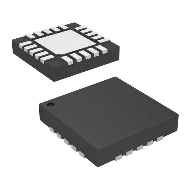
Ultra-Thin 3x3mm QFN-UT-20 package
(SX1504/SX1505)
Ultra-Thin 4x4mm QFN-UT-28 package
(SX1506)
Pb & Halogen Free, RoHS/WEEE compliant
TYPICAL APPLICATIONS
•
•
•
•
•
•
•
The SX1504, SX1505 and SX1506 have the ability to
generate mask-programmable interrupts based on
falling/rising edge of any of its GPIO lines. A
dedicated pin indicates to a host controller that a
state change occurred in one or more of the GPIO
lines.
The SX1504, SX1505 and SX1506 each come in a
small QFN-UT-20/28 package. All devices are rated
from -40°C to +85°C temperature range.
Cell phones, PDAs, MP3 players
Digital camera
Portable multimedia player
Notebooks
GPS Units
Industrial, ATE
Any battery powered equipment
ORDERING INFORMATION
(1)
Part Number
SX1504I087TRT
SX1505I087TRT
SX1506I091TRT
(1)
SX1502EVK
I/O Channels
4
8
16
8
Package
QFN-UT-20
QFN-UT-20
QFN-UT-28
Evaluation Kit
SX1502I087TRT based, unique evaluation kit for the three parts.
th
Rev 3 – 16 May 2012
www.semtech.com
1
�SX1504/SX1505/SX1506
4/8/16 Channel GPIO
WIRELESS & SENSING
Table of Contents
GENERAL DESCRIPTION ..................................................................................................................... 1
ORDERING INFORMATION................................................................................................................... 1
KEY PRODUCT FEATURES.................................................................................................................. 1
TYPICAL APPLICATIONS ..................................................................................................................... 1
1
PIN DESCRIPTION ...................................................................................................................... 4
1.1
1.2
1.3
2
SX1504 4-channel GPIO
SX1505 8-channel GPIO
SX1506 16-channel GPIO
4
5
6
ELECTRICAL CHARACTERISTICS ............................................................................................... 7
2.1
2.2
3
Absolute Maximum Ratings
Electrical Specifications
7
7
TYPICAL OPERATING CHARACTERISTICS ............................................................................... 10
3.1
3.2
3.3
4
IDDM vs. VDDM
VOL vs. IOL
VOH vs. IOH
10
10
11
BLOCK DETAILED DESCRIPTION ............................................................................................. 12
4.1
4.2
4.3
4.4
4.5
SX1504 4-channel GPIO
SX1505 8-channel GPIO
SX1506 16-channel GPIO
Reset (NRESET)
2
2-Wire Interface (I C)
4.5.1
WRITE
4.5.2
READ
4.5.3
READ - STOP separated format (SX1504 and SX1505 only)
4.6
Interrupt (NINT)
4.7
Programmable Logic Functions (PLD)
4.7.1
SX1504
4.7.2
SX1505
4.7.3
SX1506
4.7.4
Tutorial
5
CONFIGURATION REGISTERS .................................................................................................. 19
5.1
5.2
5.3
6
SX1504 4-channel GPIO
SX1505 8-channel GPIO
SX1506 16-channel GPIO
19
20
22
APPLICATION INFORMATION ................................................................................................... 26
6.1
6.2
Typical Application Circuit
Typical LED Operation
6.2.1
LED ON/OFF Control
6.2.2
LED Intensity Control
6.3
Keypad Implementation
6.4
Level Shifter Implementation Hints
7
12
12
13
13
14
14
15
15
16
16
16
17
17
18
26
26
26
27
27
27
PACKAGING INFORMATION ..................................................................................................... 28
th
Rev 3 – 16 May 2012
www.semtech.com
2
�SX1504/SX1505/SX1506
4/8/16 Channel GPIO
WIRELESS & SENSING
7.1
7.2
7.3
7.4
8
QFN-UT 20-pin Outline Drawing
QFN-UT 20-pin Land Pattern
QFN-UT 28-pin Outline Drawing
QFN-UT 28-pin Land Pattern
28
28
29
29
SOLDERING PROFILE .............................................................................................................. 30
th
Rev 3 – 16 May 2012
www.semtech.com
3
�SX1504/SX1505/SX1506
4/8/16 Channel GPIO
WIRELESS & SENSING
1
1.1
PIN DESCRIPTION
SX1504 4-channel GPIO
Pin
Symbol
Type
1
2
3
4
5
6
7
8
NRESET
SDA
NC1
SCL
I/O[0]
I/O[1]
VCC1
GND
DIO
DIO
DI
DIO (*1)
DIO (*1)
P
P
9
I/O[2]
DIO (*1)
10
I/O[3]
DIO (*1)
11
12
13
14
15
16
17
18
19
20
NINT
ADDR
NC2
VDDM
NC3
NC4
NC7
GND
NC5
NC6
DO
DI
P
P
-
Description
Active low reset
I2C serial data line
Leave open, not connected
I2C serial clock line
I/O[0], at power-on configured as an input
I/O[1], at power-on configured as an input
I/O supply voltage
Ground Pin
I/O[2], at power-on configured as an input
High sink I/O.
I/O[3], at power-on configured as an input
High sink I/O.
Active low interrupt output
Address input, connect to VDDM or GND
Leave open, not connected
Main supply voltage
Leave open, not connected
Leave open, not connected
Connect to VCC1
Ground Pin
Leave open, not connected
Leave open, not connected
A: Analog
D: Digital
I: Input
O: Output
P: Power
(*1) This pin is programmable through the I2C interface
NC4
NC7
GND
NC5
NC6
Table 1 – SX1504 Pin Description
NRESET
NC3
SDA
VDDM
NC1
NC2
SCL
ADDR
GND
(PAD)
I/O[3]
I/O[2]
GND
VCC1
NINT
I/O[1]
I/O[0]
Figure 1 – SX1504 QFN-UT-20 Pinout
th
Rev 3 – 16 May 2012
www.semtech.com
4
�SX1504/SX1505/SX1506
4/8/16 Channel GPIO
WIRELESS & SENSING
1.2
SX1505 8-channel GPIO
Pin
Symbol
Type
1
2
3
4
5
6
7
8
NRESET
SDA
NC1
SCL
I/O[0]
I/O[1]
VCC1
GND
DIO
DIO
DI
DIO (*1)
DIO (*1)
P
P
9
I/O[2]
DIO (*1)
10
I/O[3]
DIO (*1)
11
12
13
14
15
16
17
18
19
20
NINT
ADDR
NC2
VDDM
I/O[4]
I/O[5]
VCC2
GND
I/O[6]
I/O[7]
DO
DI
P
DIO (*1)
DIO (*1)
P
P
DIO (*1)
DIO (*1)
Description
Active low reset
I2C serial data line
Leave open, not connected
I2C serial clock line
I/O[0], at power-on configured as an input
I/O[1], at power-on configured as an input
Supply voltage for Bank A I/O[0-3]
Ground Pin
I/O[2], at power-on configured as an input
High sink I/O.
I/O[3], at power-on configured as an input
High sink I/O.
Active low interrupt output
Address input, connect to VDDM or GND
Leave open, not connected
Main supply voltage
I/O[4], at power-on configured as an input
I/O[5], at power-on configured as an input
Supply voltage for Bank B I/O[4-7]
Ground Pin
I/O[6], at power-on configured as an input
I/O[7], at power-on configured as an input
A: Analog
D: Digital
I: Input
O: Output
P: Power
(*1) This pin is programmable through the I2C interface
I/O[5]
VCC2
GND
I/O[6]
I/O[7]
Table 2 – SX1505 Pin Description
NRESET
I/O[4]
SDA
VDDM
NC1
NC2
SCL
ADDR
GND
(PAD)
I/O[3]
I/O[2]
GND
VCC1
NINT
I/O[1]
I/O[0]
Figure 2 – SX1505 QFN-UT-20 Pinout
th
Rev 3 – 16 May 2012
www.semtech.com
5
�SX1504/SX1505/SX1506
4/8/16 Channel GPIO
WIRELESS & SENSING
1.3
SX1506 16-channel GPIO
Pin
Symbol
Type
Description
1
2
3
4
5
6
7
GND
I/O[2]
I/O[3]
VCC1
I/O[4]
I/O[5]
GND
P
DIO (*1)
DIO (*1)
P
DIO (*1)
DIO (*1)
P
8
I/O[6]
DIO (*1)
9
I/O[7]
DIO (*1)
10
11
12
13
14
15
16
17
18
19
20
21
NINT
NC
VDDM
I/O[8]
I/O[9]
GND
I/O[10]
I/O[11]
VCC2
I/O[12]
I/O[13]
GND
DO
P
DIO (*1)
DIO (*1)
P
DIO (*1)
DIO (*1)
P
DIO (*1)
DIO (*1)
P
22
I/O[14]
DIO (*1)
23
I/O[15]
DIO (*1)
24
25
26
27
28
NRESET
SDA
SCL
I/O[0]
I/O[1]
DIO
DIO
DI
DIO (*1)
DIO (*1)
Ground Pin
I/O[2], at power-on configured as an input
I/O[3], at power-on configured as an input
I/O supply voltage for Bank A I/O[0-7]
I/O[4], at power-on configured as an input
I/O[5], at power-on configured as an input
Ground Pin
I/O[6], at power-on configured as an input
High sink I/O.
I/O[7], at power-on configured as an input
High sink I/O.
Active low interrupt output
Leave open, not connected
Main supply voltage
I/O[8], at power-on configured as an input
I/O[9], at power-on configured as an input
Ground Pin
I/O[10], at power-on configured as an input
I/O[11], at power-on configured as an input
I/O supply voltage for Bank B I/O[8-15]
I/O[12], at power-on configured as an input
I/O[13], at power-on configured as an input
Ground Pin
I/O[14], at power-on configured as an input
High sink I/O.
I/O[15], at power-on configured as an input
High sink I/O.
Active low reset
I2C serial data line
I2C serial clock line
I/O[0], at power-on configured as an input
I/O[1], at power-on configured as an input
A: Analog
D: Digital
I: Input
O: Output
P: Power
(*1) This pin is programmable through the I2C interface
22 I/O[14]
23 I/O[15]
24 NRESET
25 SDA
26 SCL
27 I/O[0]
28 I/O[1]
Table 3 – SX1506 Pin Description
I/O[12]
GND
(PAD)
18
VCC2
I/O[4] 5
17
I/O[11]
I/O[5] 6
16
I/O[10]
GND 7
15
GND
8
9
10
I/O[6]
I/O[7]
NINT
VCC1 4
14
19
I/O[9]
TOP VIEW
I/O[3] 3
13
I/O[13]
I/O[8]
20
12
I/O[2] 2
VDDM
GND
11
21
NC
GND 1
Figure 3 – SX1506 QFN-UT-28 Pinout
th
Rev 3 – 16 May 2012
www.semtech.com
6
�SX1504/SX1505/SX1506
4/8/16 Channel GPIO
WIRELESS & SENSING
2
ELECTRICAL CHARACTERISTICS
2.1
Absolute Maximum Ratings
Stress above the limits listed in the following table may cause permanent failure. Exposure to absolute ratings for
extended time periods may affect device reliability. The limiting values are in accordance with the Absolute
Maximum Rating System (IEC 134). All voltages are referenced to ground (GND).
Symbol
VDDMmax
VCC1,2max
VESD_HBM
VESD_CDM
VESD_MM
TA
TC
TSTG
Ilat
Description
Main supply voltage
I/O banks supply voltage
(1)
Electrostatic handling HBM model
Electrostatic handling CDM model
Electrostatic handling MM model
Operating Ambient Temperature Range
Junction Temperature Range
Storage Temperature Range
(2)
Latchup-free input pin current
Min
- 0.4
- 0.4
-40
-40
-55
+/-100
Max
6.0
6.0
1500
300
200
+85
+125
+150
-
Unit
V
V
V
V
V
°C
°C
°C
mA
(1) Tested according to JESD22-A114A
(2) Static latch-up values are valid at maximum temperature according to JEDEC 78 specification
Table 4 - Absolute Maximum Ratings
2.2
Electrical Specifications
Table below applies to default registers values, unless otherwise specified. Typical values are given for TA =
+25°C, VDDM=VCC1=VCC2=3.3V.
Symbol
Supply
VDDM
VCC1,2
Description
Conditions
Min
Typ
Max
Unit
-
2.5
2.5
-
5.5
5.5
V
V
-
-
1
5
µA
-
-
1
2
µA
Main supply voltage
I/O banks supply voltage
Main supply current
IDDM
2
(I C inactive)
(1)
ICC1,2 I/O banks supply current
I/Os set as Input
VIH
High level input voltage
-
0.7*
VCC1,2
-
VIL
Low level input voltage
-
-0.4
-
VHYS
Hysteresis of Schmitt trigger
-
-
0.1*
VCC1,2
-
V
ILEAK
Input leakage current
-1.5
-
1.5
µA
-
-
10
pF
CI
Input capacitance
I/Os set as Output
VOH
Assuming no active
pull-up/down
-
Interrupt reset timing
V
-
VCC1,2
V
-
-
0.3
V
-
-
-
8
mA
-
-
-
24
mA
-
-
-
12
mA
Cf. Figure 9
-
-
1.5
µs
From input data change
From RegInterruptSource
clearing
-
-
0.3
12
1
V
mA
µs
-
-
2
µs
-
VOL
tIR
V
VCC1,2
– 0.3
-0.4
High level output voltage
Low level output voltage
High level output source
IOH
current
Low level output sink current
for the high sink I/Os
IOL
Low level output sink current
for the other I/Os.
tPV
Output data valid timing
NINT (Output)
VOL
Low level output voltage
IOLM
Low level output sink current
tIV
Interrupt valid timing
VCC1,2
+0.3
0.3*
VCC1,2
th
Rev 3 – 16 May 2012
www.semtech.com
7
�SX1504/SX1505/SX1506
4/8/16 Channel GPIO
WIRELESS & SENSING
Symbol Description
NRESET (Input/Output)
VOL
Low level output voltage
IOLM
Low level output sink current
Conditions
Min
Typ
Max
Unit
-
0.7*
VDDM
-
0.3
12
V
mA
-
5.5
V
-
0.3*
VDDM
V
-
V
VIHMR
High level input voltage
-
VILM
Low level input voltage
-
-0.4
Hysteresis of Schmitt trigger
-
-
Cf. Figure 7
Cf. Figure 7
Cf. Figure 7
Cf. Figure 7
Cf. Figure 7
-1.5
0.7
300
VHYSM
ILEAK Input leakage current
CI
Input capacitance
VPOR Power-On-Reset voltage
VDROPH High brown-out voltage
VDROPL Low brown-out voltage
tRESET
Reset time
tPULSE
Reset pulse from host uC
ADDR (Input)
0.1*
VDDM
VDDM-1
0.2
-
VIHMA
High level input voltage
-
0.7*
VDDM
-
VILM
Low level input voltage
-
-0.4
-
Hysteresis of Schmitt trigger
-
-
VHYSM
1.5
10
0.9
7
VDDM
+0.3
0.3*
VDDM
0.1*
VDDM
-
-
µA
pF
V
V
V
ms
ns
V
V
V
ILEAK Input leakage current
-1.5
1.5
µA
CI
Input capacitance
10
pF
(2)
SCL (Input) and SDA (Input/Output)
2
2
Interface complies with slave F/S mode I C interface as described by Philips I C specification version 2.1
2
dated January, 2000. Please refer to that document for more detailed I C specifications.
VOL
IOLM
Low level output voltage
Low level output sink current
-
VIHMR
High level input voltage
-
VILM
Low level input voltage
fSCL
SCL clock frequency
Hold time (repeated) START
condition
LOW period of the SCL clock
HIGH period of the SCL clock
Set-up time for a repeated
START condition
Data hold time
Data set-up time
Rise time of both SDA and
SCL signals
Fall time of both SDA and
SCL signals
Set-up time for STOP
condition
tHD;STA
tLOW
tHIGH
tSU;STA
tHD;DAT
tSU;DAT
tr
tf
tSU;STO
0.7*
VDDM
-
0.3
12
V
mA
-
5.5
V
-
-0.4
-
-
0
-
-
0.3*
VDDM
400
kHz
0.6
-
-
µs
-
1.3
0.6
-
-
µs
µs
-
0.6
-
-
-
(3)
th
0.9
-
µs
(6)
-
300
ns
(6)
-
300
ns
-
-
µs
20+0.1Cb
-
20+0.1Cb
0.6
µs
(4)
-
-
-
Rev 3 – 16 May 2012
0
(5)
100
V
www.semtech.com
8
�SX1504/SX1505/SX1506
4/8/16 Channel GPIO
WIRELESS & SENSING
Symbol
Description
Bus free time between a
tBUF
STOP and START condition
Capacitive load for each bus
Cb
line
Noise margin at the LOW
VnL
level for each connected
device (including hysteresis)
Noise margin at the HIGH
VnH
level for each connected
device (including hysteresis)
Miscellaneous
Programmable pull-up/down
RPULL
resistors for IO[0-7]
tPLD
PLD propagation delay
Conditions
Min
Typ
Max
Unit
-
1.3
-
-
µs
-
-
-
400
pF
-
0.1*VDDM
-
-
V
-
0.2*VDDM
-
-
V
-
-
60
-
kΩ
VCC1,2 & VDDM = 5V
-
-
25
ns
(1) Assuming no load connected to outputs and inputs fixed to VCC1,2 or GND.
(2) All values referred to VIHMR min and VILM max levels.
(3) A device must internally provide a hold time of at least 300ns for the SDA signal (referred to VIHMR min) to bridge the undefined region of
the falling edge of SCL.
(4) The maximum tHD;DAT has only to be met if the device does not stretch the LOW period (tLOW ) of the SCL signal.
(5) A Fast-mode I2C-bus device can be used in a Standard-mode I2C-bus system, but the requirement tSU;DAT ≥ 250 ns must then be met.
This will automatically be the case if the device does not stretch the LOW period of the SCL signal.
If such a device does stretch the LOW period of the SCL signal, it must output the next data bit to the SDA line tr max+ tSU;DAT = 1000 + 250
= 1250 ns (according to the Standard-mode I2C-bus specification) before the SCL line is released.
(6) Cb = total capacitance of one bus line in pF. If mixed with Hs-mode devices, faster fall-times are allowed.
Table 5 – Electrical Specifications
th
Rev 3 – 16 May 2012
www.semtech.com
9
�SX1504/SX1505/SX1506
4/8/16 Channel GPIO
WIRELESS & SENSING
3
TYPICAL OPERATING CHARACTERISTICS
Figures below apply to default registers values, Tamb, unless otherwise specified.
3.1
IDDM vs. VDDM
IDDM vs VDDM
3.5
3
2.5
IDDM (uA)2
90°C
-40°C
1.5
1
0.5
0
0
1
2
3
4
5
6
VDDM (V)
3.2
VOL vs. IOL
VOL vs IOL (VCC1,2=5.5V, High Sink IOs)
0.15
0.1
VOL (V)
*
Tamb
0.05
0
0
*
5
Doesn’t vary significantly with temperature
10
15
20
25
30
IOL (mA)
th
Rev 3 – 16 May 2012
www.semtech.com
10
�SX1504/SX1505/SX1506
4/8/16 Channel GPIO
WIRELESS & SENSING
3.3
VOH vs. IOH
VOH vs IOH (VCC1,2=5.5V)
5.5
5.4
5.3
VOH (V)
Tamb
*
5.2
5.1
5
0
*
Doesn’t vary significantly with temperature
10
20
IOH (mA)
th
Rev 3 – 16 May 2012
www.semtech.com
11
�SX1504/SX1505/SX1506
4/8/16 Channel GPIO
WIRELESS & SENSING
4
4.1
BLOCK DETAILED DESCRIPTION
SX1504 4-channel GPIO
VDDM
Reset
NRESET
2
I C Bus
Control
SCL
SDA
4-Bit
R/W
I/O Bank A
A
Input
VCC1
I/O[0]
I/O[1]
I/O[2]
I/O[3]
Filter
Interrupt
NINT
I/O Bank A
VCC1
I/O[0]
I/O[1]
I/O[2]
I/O[3]
ADDR
SX1504
GND
Figure 4 – SX1504 Block Diagram
4.2
SX1505 8-channel GPIO
VDDM
Reset
NRESET
SCL
SDA
A
2
I C Bus
8-Bit
Control
R/W
Input
I/O Bank B
Filter
A
VCC2
I/O[4]
I/O[5]
I/O[6]
I/O[7]
ADDR
SX1505
Interrupt
NINT
GND
Figure 5 – SX1505 Block Diagram
th
Rev 3 – 16 May 2012
www.semtech.com
12
�SX1504/SX1505/SX1506
4/8/16 Channel GPIO
WIRELESS & SENSING
4.3
SX1506 16-channel GPIO
VCC1
I/O[0]
I/O[1]
I/O[2]
I/O[3]
I/O[4]
I/O[5]
I/O[6]
I/O[7]
I/O Bank A
VDDM
A
8-Bit
Reset
R/W
NRESET
2
I C Bus
Control
SCL
SDA
Input
8-Bit
Filter
R/W
VCC2
I/O[8]
I/O[9]
I/O[10]
I/O[11]
I/O[12]
I/O[13]
I/O[14]
I/O[15]
I/O Bank B
A
SX1506
NINT
Interrupt
GND
Figure 6 – SX1506 Block Diagram
4.4
Reset (NRESET)
The SX1504, SX1505 and SX1506 generate their own power on reset signal after a power supply is connected
to the VDDM pin. The reset signal is made available for the user at the pin NRESET. The rising edge of the
NRESET indicates that the startup sequence of the SX1504, SX1505 or SX1506 has finished. NRESET must be
connected to VDDM (or greater) either directly, or via a resistor.
1
2
3
4
5
6
2
1
VDROPH
VPOR
VDROPL
VDDM
Undefined
Undefined
Undefined
NRESET
tRESET
tPULSE
tRESET
Figure 7 – Power-On / Brown-out Reset Conditions
1. Device behavior is undefined until VDDM rises above VPOR, at which point NRESET is driven to GND
by the SX1504, SX1505 or SX1506.
2. After tRESET, NRESET is released (high-impedance) by the SX1504, SX1505 or SX1506 to allow it to be
pulled high by an external resistor.
3. In operation, the SX1504, SX1505 and SX1506 may be reset at anytime by an external device driving
NRESET low during tPULSE. Chip can be accessed normally again after NRESET rising edge.
th
Rev 3 – 16 May 2012
www.semtech.com
13
�SX1504/SX1505/SX1506
4/8/16 Channel GPIO
WIRELESS & SENSING
4. During a brown-out event, if VDDM drops above VDROPH a reset will not occur.
5. During a brown-out event, if VDDM drops between VDROPH and VDROPL a reset may occur.
6. During a brown-out event, if VDDM drops below VDROPL a reset will occur next time VPOR is crossed.
Please note that a brown-out event is defined as a transient event on VDDM. If VDDM is attached to a battery,
then the gradual decay of the battery voltage will not be interpreted as a brown-out event.
Please also note that a sharp rise in VDDM (> 1V/us) may induce a circuit reset.
2
4.5
2-Wire Interface (I C)
2
The SX1504, SX1505 and SX1506 2-wire interface (I C compliant) operates only in slave mode. In this
configuration, the device has one or two device addresses defined by ADDR pin.
Device
SX1504 &
SX1505
SX1506
ADDR Pin
0
1
2
I C Address
Description
First address of the 2-wire interface
0x20 (0100000)
Second address of the 2-wire interface
0x21 (0100001)
0x20 (0100000)
Fixed address of the 2-wire interface
Table 6 - 2-Wire Interface Address
2 lines are used to exchange data between an external master host and the slave device:
• SCL : Serial CLock
• SDA : Serial DAta
2
2
The SX1504, SX1505 and SX1506 are read-write slave-mode I C devices and comply with the Philips I C
standard Version 2.1 dated January, 2000. The SX1504, SX1505 and SX1506 have respectively 12, 16, and 31
2
user-accessible internal 8-bit registers. The I C interface has been designed for program flexibility, in that once
the slave address has been sent to the SX1504, SX1505 or SX1506 enabling it to be a slave
transmitter/receiver, any register can be written or read independently of each other. While there is no auto
2
increment/decrement capability in the SX1504 and SX1505 I C logic, a tight software loop can be designed to
access the next register independent of which register you begin accessing. SX1506 implements auto increment
capability. The start and stop commands frame the data-packet and the repeat start condition is allowed if
necessary.
Seven bit addressing is used and ten bit addressing is not allowed. Any general call address will be ignored by
the SX1504, SX1505 and SX1506. The SX1504, SX1505 and SX1506 are not CBUS compatible and can
operate in standard mode (100kbit/s) or fast mode (400kbit/s).
4.5.1 WRITE
2
The simplest format for an I C write is given below. After the start condition [S], the slave address is sent,
2
followed by an eighth bit indicating a write. The I C then acknowledges that it is being addressed, and the master
responds with an 8 bit data byte consisting of the register address. The slave acknowledges and the master
sends the appropriate 8 bit data byte. Once again the slave acknowledges and the master terminates the
transfer with the stop condition [P].
Master operations
SX1504, SX1505 or SX1506 operations (Slave)
S: Start Condition
W: Write = ‘0’
A: Acknowledge (sent by slave)
P: Stop condition
Slave Address: 7 bit
Register Address: 8 bit
Data: 8 bit
Figure 8 - 2-Wire Serial Interface, Write Register Operation
th
Rev 3 – 16 May 2012
www.semtech.com
14
�SX1504/SX1505/SX1506
4/8/16 Channel GPIO
WIRELESS & SENSING
Figure 9 – Write RegData Register
Please note that SX1506 implements register address auto-increment i.e. after the Data ACK from Slave the
master can write further bytes and the interface will handle the register address increment automatically. Finally
the master terminates the transfer normally the stop condition [P].
4.5.2
READ
2
After the start condition [S], the slave address is sent, followed by an eighth bit indicating a write. The I C then
acknowledges that it is being addressed, and the master responds with an 8 bit data byte consisting of the
register address. The slave acknowledges and the master sends the repeated start condition [Sr]. Once again,
the slave address is sent, followed by an eighth bit indicating a read. The slave responds with an acknowledge
and the previously addressed 8 bit data byte; the master then sends a non-acknowledge (NACK). Finally, the
master terminates the transfer with the stop condition [P].
Master operations
SX1504, SX1505 or SX1506 operations (Slave)
S: Start Condition
W: Write = ‘0’
R: Read = ‘1’
A: Acknowledge (sent by slave)
NACK: Non-Acknowledge (sent by master)
Sr: Repeated Start Condition
P: Stop condition
Slave Address: 7 bit
Register Address: 8 bit
Data: 8 bit
Figure 10 - 2-Wire Serial Interface, Read Register Operation
Please note that SX1506 implements register address auto-increment i.e. after the Data byte from Slave the
master can acknowledge (ACK) to indicate that it wants to read the next byte and the interface will handle the
register address increment automatically. Finally the master terminates the transfer normally with a NACK
followed by the stop condition [P].
4.5.3 READ - STOP separated format (SX1504 and SX1505 only)
When operating SX1504 or SX1505, stop-separated reads can also be used. This format allows a master to set
up the register address pointer for a read and return to that slave at a later time to read the data. In this format
the slave address followed by a write command are sent after a start [S] condition. The slave then acknowledges
it is being addressed, and the master responds with the 8-bit register address. The master sends a Stop or
Restart condition and may then address another slave. After performing other tasks, the master can send a start
or restart condition to the slave with a read command. The slave acknowledges this request and returns the data
from the register location that had previously been set up.
th
Rev 3 – 16 May 2012
www.semtech.com
15
�SX1504/SX1505/SX1506
4/8/16 Channel GPIO
WIRELESS & SENSING
Master operations
SX1504, SX1505 or SX1506 operations (Slave)
S: Start Condition
W: Write = ‘0’
R: Read = ‘1’
A: Acknowledge (sent by slave)
NACK: Non-Acknowledge (sent by master)
Sr: Repeated Start Condition
P: Stop condition
Slave Address: 7 bit
Register Address: 8 bit
Data: 8 bit
Figure 11 - 2-Wire Serial Interface, Read – Stop Separated Mode Operation
4.6
Interrupt (NINT)
At start-up, the transition detection logic is reset, and NINT is released to a high-impedance state. The interrupt
mask register is set to 0xFF, disabling the interrupt output for transitions on all I/O ports. The transition flags are
cleared to indicate no data changes.
An interrupt NINT can be generated on any programmed combination of I/Os rising and/or falling edges through
the RegInterruptMask and RegSense registers.
If needed, the I/Os which triggered the interrupt can then be identified by reading RegInterruptSource register.
When NINT is low (i.e. interrupt occurred), it can be reset back high (i.e. cleared) by writing 0xFF in
RegInterruptSource (this will also clear corresponding bits in RegEventStatus register).
SX1506 also allows the interrupt to be cleared automatically when reading RegData register (Cf. RegAdvanced)
Example: We want to detect rising edge of I/O[1] on SX1505 (NINT will go low).
1. We enable interrupt on I/O[1] in RegInterruptMask
� RegInterruptMask =“XXXXXX0X”
2. We set edge sense for I/O[1] in RegSense
� RegSenseLow =“XXXX01XX”
4.7
Programmable Logic Functions (PLD)
The SX1504, SX1505 and SX1506 offer a unique fully programmable logic functions like a PLD to give more
flexibility and reduce external logic gates used for standard applications.
Since the whole truth table is fully programmable, the SX1504, SX1505, and SX1506 can implement
combinatory functions ranging from the basic AND/OR gates to the most complicated ones with up to four 3-to1
PLDs or two 3-to-2 PLDs which can also be externally cascaded if needed.
In all cases, any IO not configured for PLD functionality retains its GPIO functionality while I/Os used by the PLD
have their direction automatically set accordingly.
Please note that while RegDir corresponding bits are ignored for PLD operation they may still be set to input to
access unused PLD inputs as normal GPI (PLD truth table can define some inputs to have no effect on PLD
output) and/or generate interrupt based on any of the PLD inputs or outputs bits.
4.7.1 SX1504
The SX1504 I/Os can be configured to provide any combinational 2-to-1 logic function using I/O[0-2] whilst
retaining GPIO capability on I/O[3] OR provide a combinational 3-to-1 decode function using all 4 I/O ports.
RegPLDMode
SX1504 I/Os
1:0
3
2
1
00
GPIO
GPIO
GPIO
01
GPIO PLD OUT PLD IN
10
PLD OUT PLD IN PLD IN
Table 7 – SX1504 PLD Modes Settings
th
Rev 3 – 16 May 2012
0
GPIO
PLD IN
PLD IN
www.semtech.com
16
�SX1504/SX1505/SX1506
4/8/16 Channel GPIO
WIRELESS & SENSING
4.7.2
SX1505
The SX1505 I/Os can be configured as per the SX1504, and can additionally be configured to provide a 2-to-1
logic function on I/O[4-6], 3-to-1 logic function on I/O[4-7], or 3-to-2 logic decode on I/O[0-4].
RegPLDMode
5:4
1:0
00
00
00
01
00
10
00
11
01
00
01
01
01
10
01
11
10
00
10
01
10
10
10
11
SX1505 I/Os
7
6
5
4
3
2
GPIO
GPIO
GPIO
GPIO
GPIO
GPIO
GPIO
GPIO
GPIO
GPIO
GPIO PLD OUT
GPIO
GPIO
GPIO
GPIO PLD OUT PLD IN
GPIO
GPIO
GPIO PLD OUT PLD OUT PLD IN
GPIO PLD OUT PLD IN PLD IN
GPIO
GPIO
GPIO PLD OUT PLD IN PLD IN
GPIO PLD OUT
GPIO PLD OUT PLD IN PLD IN PLD OUT PLD IN
GPIO
GPIO
GPIO PLD OUT PLD OUT PLD IN
PLD OUT PLD IN PLD IN PLD IN
GPIO
GPIO
PLD OUT PLD IN PLD IN PLD IN
GPIO PLD OUT
PLD OUT PLD IN PLD IN PLD IN PLD OUT PLD IN
GPIO
GPIO
GPIO PLD OUT PLD OUT PLD IN
Table 8 – SX1505 PLD Modes Settings
1
GPIO
PLD IN
PLD IN
PLD IN
GPIO
PLD IN
PLD IN
PLD IN
GPIO
PLD IN
PLD IN
PLD IN
0
GPIO
PLD IN
PLD IN
PLD IN
GPIO
PLD IN
PLD IN
PLD IN
GPIO
PLD IN
PLD IN
PLD IN
SX1506 I/Os
15
14
13
12
11
10
GPIO
GPIO
GPIO
GPIO
GPIO
GPIO
GPIO
GPIO
GPIO
GPIO
GPIO PLD OUT
GPIO
GPIO
GPIO
GPIO PLD OUT PLD IN
GPIO
GPIO
GPIO PLD OUT PLD OUT PLD IN
GPIO PLD OUT PLD IN PLD IN
GPIO
GPIO
GPIO PLD OUT PLD IN PLD IN
GPIO PLD OUT
GPIO PLD OUT PLD IN PLD IN PLD OUT PLD IN
GPIO
GPIO
GPIO PLD OUT PLD OUT PLD IN
PLD OUT PLD IN PLD IN PLD IN
GPIO
GPIO
PLD OUT PLD IN PLD IN PLD IN
GPIO PLD OUT
PLD OUT PLD IN PLD IN PLD IN PLD OUT PLD IN
GPIO
GPIO
GPIO PLD OUT PLD OUT PLD IN
Table 9 – SX1506 PLD Modes Settings (Bank B)
9
GPIO
PLD IN
PLD IN
PLD IN
GPIO
PLD IN
PLD IN
PLD IN
GPIO
PLD IN
PLD IN
PLD IN
8
GPIO
PLD IN
PLD IN
PLD IN
GPIO
PLD IN
PLD IN
PLD IN
GPIO
PLD IN
PLD IN
PLD IN
RegPLDModeA
SX1506 I/Os
5:4
1:0
7
6
5
4
3
2
00
00
GPIO
GPIO
GPIO
GPIO
GPIO
GPIO
00
01
GPIO
GPIO
GPIO
GPIO
GPIO PLD OUT
00
10
GPIO
GPIO
GPIO
GPIO PLD OUT PLD IN
00
11
GPIO
GPIO
GPIO PLD OUT PLD OUT PLD IN
01
00
GPIO PLD OUT PLD IN PLD IN
GPIO
GPIO
01
01
GPIO PLD OUT PLD IN PLD IN
GPIO PLD OUT
01
10
GPIO PLD OUT PLD IN PLD IN PLD OUT PLD IN
01
11
GPIO
GPIO
GPIO PLD OUT PLD OUT PLD IN
10
00
PLD OUT PLD IN PLD IN PLD IN
GPIO
GPIO
10
01
PLD OUT PLD IN PLD IN PLD IN
GPIO PLD OUT
10
10
PLD OUT PLD IN PLD IN PLD IN PLD OUT PLD IN
10
11
GPIO
GPIO
GPIO PLD OUT PLD OUT PLD IN
Table 10 – SX1506 PLD Modes Settings (Bank B)
1
GPIO
PLD IN
PLD IN
PLD IN
GPIO
PLD IN
PLD IN
PLD IN
GPIO
PLD IN
PLD IN
PLD IN
0
GPIO
PLD IN
PLD IN
PLD IN
GPIO
PLD IN
PLD IN
PLD IN
GPIO
PLD IN
PLD IN
PLD IN
4.7.3 SX1506
Each of the two I/O banks of the SX1506 I/Os can be configured as per the SX1505.
RegPLDModeB
5:4
1:0
00
00
00
01
00
10
00
11
01
00
01
01
01
10
01
11
10
00
10
01
10
10
10
11
th
Rev 3 – 16 May 2012
www.semtech.com
17
�SX1504/SX1505/SX1506
4/8/16 Channel GPIO
WIRELESS & SENSING
4.7.4 Tutorial
The generic method described in this paragraph can be applied to any of the SX1504, SX1505 or SX1506.
Example: We want to implement an AND gate between I/O[0] and IO[1] on SX1505
1. Identify in the tables above the RegPLDMode setting to be programmed.
What we need corresponds to the second line of the SX1505 PLD Table => RegPLDMode = “xx00xx01”
2. Fill corresponding RegPLDTableX with the wanted truth table.
As mentioned in RegPLDMode description, using PLD 2-to-1 mode on I/0[0-2] implies to fill the truth
table located in RegPLDTable0(3:0)
I/O[1]
0
0
1
1
I/O[0]
0
1
0
1
I/O[2]
0
0
0
1
=> RegPLDTable0 = “xxxx1000”
th
Rev 3 – 16 May 2012
www.semtech.com
18
�SX1504/SX1505/SX1506
4/8/16 Channel GPIO
WIRELESS & SENSING
5
5.1
CONFIGURATION REGISTERS
SX1504 4-channel GPIO
Address
0x00
0x01
0x02
0x03
0x04
0x05
0x06
0x07
0x08
0x09
0x10
0x11
0x12
0x13
0x14
0x15
Name
Description
RegData
RegDir
RegPullUp
RegPullDown
Reserved
RegInterruptMask
RegSenseHigh
RegSenseLow
RegInterruptSource
RegEventStatus
RegPLDMode
RegPLDTable0
RegPLDTable1
RegPLDTable2
RegPLDTable3
RegPLDTable4
Data register
Direction register
Pull-up register
Pull-down register
Unused
Interrupt mask register
Unused
Sense register
Interrupt source register
Event status register
PLD mode register
PLD truth table 0
Unused
PLD truth table 2
Unused
Unused
Default
1111 1111*
1111 1111
0000 0000
0000 0000
XXXX XXXX
1111 1111
XXXX XXXX
0000 0000
0000 0000
0000 0000
0000 0000
0000 0000
XXXX XXXX
0000 0000
XXXX XXXX
XXXX XXXX
*Bits set as output take “1” as default value.
Table 11 – SX1504 Configuration Registers Overview
Addr
Name
Default
Bits
7:4
0x00
RegData
0xFF
3:0
7:4
0x01
RegDir
0xFF
0x02
RegPullUp
0x00
0x03
RegPullDown
0x00
0x04
Reserved
0xXX
0x05
RegInterruptMask
0xFF
0x06
RegSenseHigh
0xXX
0x07
RegSenseLow
0x00
3:0
7:4
3:0
7:4
0x08
RegInterruptSource
0x09
0x00
0x00
3:0
7:0
7:4
3:0
7:0
7:6
5:4
3:2
1:0
7:4
Description
Reserved. Must be set to 1 (default value)
Write: Data to be output to the output-configured IOs
Read: Data seen at the IOs, independent of the direction configured.
Reserved. Must be set to 1 (default value)
Configures direction for each IO.
0 : IO is configured as an output
1 : IO is configured as an input
Reserved. Must be set to 0 (default value)
Enables the pull-up for each IO
0 : Pull-up is disabled
1 : Pull-up is enabled
Reserved. Must be set to 0 (default value)
Enables the pull-down for each IO
0 : Pull-down is disabled
1 : Pull-down is enabled
Unused
Reserved. Must be set to 1 (default value)
Configures which [input-configured] IO will trigger an interrupt on NINT pin
0 : An event on this IO will trigger an interrupt
1 : An event on this IO will NOT trigger an interrupt
Unused
Edge sensitivity of I/O[3]
00 : None
Edge sensitivity of I/O[2]
01 : Rising
10 : Falling
Edge sensitivity of I/O[1]
11 : Both
Edge sensitivity of I/O[0]
3:0
Reserved. Must be set to 0 (default value)
Interrupt source (from IOs set in RegInterruptMask)
0 : No interrupt has been triggered by this IO
1 : An interrupt has been triggered by this IO (an event as configured in relevant
RegSense register occured).
7:4
Writing '1' clears the bit in RegInterruptSource and in RegEventStatus.
When all bits are cleared, NINT signal goes back high.
Reserved. Must be set to 0 (default value)
th
Rev 3 – 16 May 2012
www.semtech.com
19
�SX1504/SX1505/SX1506
4/8/16 Channel GPIO
WIRELESS & SENSING
Addr
Name
Default
Bits
RegEventStatus
3:0
7:2
0x10
0x00
RegPLDMode
0x11
RegPLDTable0
0x00
0x12
RegPLDTable1
0xXX
0x13
RegPLDTable2
0x00
0x14
0x15
RegPLDTable3
RegPLDTable4
0xXX
0xXX
1:0
7:4
3
2
1
0
7:0
7
6
5
4
3
2
1
0
7:0
7:0
Description
Event status of all IOs.
0 : No event has occured on this IO
1 : An event has occured on this IO (an edge as configured in relevant RegSense
register occured).
Writing '1' clears the bit in RegEventStatus and in RegInterruptSource if relevant.
If the edge sensitivity of the IO is changed, the bit(s) will be cleared automatically
Reserved. Must be set to 0 (default value)
PLDMode
00 : PLD disabled – Normal GPIO mode for I/O[3:0]
01 : PLD 2-to-1 mode – I/O[2] is a decode of I/O[1:0] as defined in RegPLDTable0
10 : PLD 3-to-1 mode – I/O[3] is a decode of I/O[2:0] as defined in RegPLDTable2
11 : Not used
Reserved. Must be set to 0 (default value)
Value to be output on I/O[2] when I/O[1:0] = 11
Value to be output on I/O[2] when I/O[1:0] = 10
Applies only when PLDMode is
set to PLD 2-to-1 mode
Value to be output on I/O[2] when I/O[1:0] = 01
Value to be output on I/O[2] when I/O[1:0] = 00
Unused
Value to be output on I/O[3] when I/O[2:0] = 111
Value to be output on I/O[3] when I/O[2:0] = 110
Value to be output on I/O[3] when I/O[2:0] = 101
Value to be output on I/O[3] when I/O[2:0] = 100
Value to be output on I/O[3] when I/O[2:0] = 011
Value to be output on I/O[3] when I/O[2:0] = 010
Value to be output on I/O[3] when I/O[2:0] = 001
Value to be output on I/O[3] when I/O[2:0] = 000
Unused
Unused
Applies only when PLDMode is
set to PLD 3-to-1 mode
Table 12 – SX1504 Configuration Registers Description
5.2
SX1505 8-channel GPIO
Address
0x00
0x01
0x02
0x03
0x04
0x05
0x06
0x07
0x08
0x09
0x10
0x11
0x12
0x13
0x14
0x15
Name
Description
RegData
RegDir
RegPullUp
RegPullDown
Reserved
RegInterruptMask
RegSenseHigh
RegSenseLow
RegInterruptSource
RegEventStatus
RegPLDMode
RegPLDTable0
RegPLDTable1
RegPLDTable2
RegPLDTable3
RegPLDTable4
Data register
Direction register
Pull-up register
Pull-down register
Unused
Interrupt mask register
Sense register for I/O[7:4]
Sense register for I/O[3:0]
Interrupt source register
Event status register
PLD mode register
PLD truth table 0
PLD truth table 1
PLD truth table 2
PLD truth table 3
PLD truth table 4
Default
1111 1111*
1111 1111
0000 0000
0000 0000
XXXX XXXX
1111 1111
0000 0000
0000 0000
0000 0000
0000 0000
0000 0000
0000 0000
0000 0000
0000 0000
0000 0000
0000 0000
*Bits set as output take “1” as default value.
Table 13 – SX1505 Configuration Registers Overview
Addr
Name
Default
Bits
0x00
RegData
0xFF
7:0
0x01
RegDir
0xFF
7:0
0x02
RegPullUp
0x00
7:0
0x03
RegPullDown
0x00
7:0
Description
Write: Data to be output to the output-configured IOs
Read: Data seen at the IOs, independent of the direction configured.
Configures direction for each IO.
0 : IO is configured as an output
1 : IO is configured as an input
Enables the pull-up for each IO
0 : Pull-up is disabled
1 : Pull-up is enabled
Enables the pull-down for each IO
0 : Pull-down is disabled
1 : Pull-down is enabled
th
Rev 3 – 16 May 2012
www.semtech.com
20
�SX1504/SX1505/SX1506
4/8/16 Channel GPIO
WIRELESS & SENSING
Addr
Default
Bits
0x04
Reserved
0xXX
7:0
0x05
RegInterruptMask
0xFF
7:0
0x06
Name
RegSenseHigh
0x00
0x07
RegSenseLow
0x00
0x08
RegInterruptSource
0x00
0x09
RegEventStatus
0x00
7:6
5:4
3:2
1:0
7:6
5:4
3:2
1:0
7:0
7:0
Writing '1' clears the bit in RegInterruptSource and in RegEventStatus
When all bits are cleared, NINT signal goes back high.
Event status of all IOs.
0 : No event has occured on this IO
1 : An event has occured on this IO (an edge as configured in relevant RegSense
register occured).
5:4
RegPLDMode
0x00
3:2
1:0
0x11
RegPLDTable0
0x00
0x12
RegPLDTable1
0x00
0x13
RegPLDTable2
0x00
0x14
RegPLDTable3
0x00
Unused
Configures which [input-configured] IO will trigger an interrupt on NINT pin
0 : An event on this IO will trigger an interrupt
1 : An event on this IO will NOT trigger an interrupt
Edge sensitivity of I/O[7]
00 : None
Edge sensitivity of I/O[6]
01 : Rising
10 : Falling
Edge sensitivity of I/O[5]
11 : Both
Edge sensitivity of I/O[4]
Edge sensitivity of I/O[3]
00 : None
Edge sensitivity of I/O[2]
01 : Rising
10 : Falling
Edge sensitivity of I/O[1]
11 : Both
Edge sensitivity of I/O[0]
Interrupt source (from IOs set in RegInterruptMask)
0 : No interrupt has been triggered by this IO
1 : An interrupt has been triggered by this IO (an event as configured in relevant
RegSense register occured).
7:6
0x10
Description
7
6
5
4
3
2
1
0
7
6
5
4
3
2
1
0
7
6
5
4
3
2
1
0
7
6
5
Writing '1' clears the bit in RegEventStatus and in RegInterruptSource if relevant.
If the edge sensitivity of the IO is changed, the bit(s) will be cleared automatically
Reserved. Must be set to 0 (default value)
PLDModeHigh (applies to I/O[7:4])
00 : PLD disabled – Normal GPIO mode for I/O[7:4]
01 : PLD 2-to-1 mode – I/O[6] is a decode of I/O[5:4] as defined in RegPLDTable0
10 : PLD 3-to-1 mode – I/O[7] is a decode of I/O[6:4] as defined in RegPLDTable1
11 : Reserved
Reserved. Must be set to 0 (default value)
PLDModeLow (applies to I/O[3:0])
00 : PLD disabled – Normal GPIO mode for I/O[3:0]
01 : PLD 2-to-1 mode – I/O[2] is a decode of I/O[1:0] as defined in RegPLDTable0
10 : PLD 3-to-1 mode – I/O[3] is a decode of I/O[2:0] as defined in RegPLDTable2
11 : PLD 3-to-2 mode – I/O[4:3] are decodes of I/O[2:0] as defined in RegPLDTable3
and RegPLDTable4
Value to be output on I/O[6] when I/O[5:4] = 11
Applies only when
Value to be output on I/O[6] when I/O[5:4] = 10
PLDModeHigh is set to PLD 2Value to be output on I/O[6] when I/O[5:4] = 01
to-1 mode
Value to be output on I/O[6] when I/O[5:4] = 00
Value to be output on I/O[2] when I/O[1:0] = 11
Applies only when
Value to be output on I/O[2] when I/O[1:0] = 10
PLDModeLow is set to PLD 2Value to be output on I/O[2] when I/O[1:0] = 01
to-1 mode
Value to be output on I/O[2] when I/O[1:0] = 00
Value to be output on I/O[7] when I/O[6:4] = 111
Value to be output on I/O[7] when I/O[6:4] = 110
Value to be output on I/O[7] when I/O[6:4] = 101
Applies only when
Value to be output on I/O[7] when I/O[6:4] = 100
PLDModeHigh is set to PLD 3Value to be output on I/O[7] when I/O[6:4] = 011
to-1 mode
Value to be output on I/O[7] when I/O[6:4] = 010
Value to be output on I/O[7] when I/O[6:4] = 001
Value to be output on I/O[7] when I/O[6:4] = 000
Value to be output on I/O[3] when I/O[2:0] = 111
Value to be output on I/O[3] when I/O[2:0] = 110
Value to be output on I/O[3] when I/O[2:0] = 101
Applies only when
Value to be output on I/O[3] when I/O[2:0] = 100
PLDModeLow is set to PLD 3Value to be output on I/O[3] when I/O[2:0] = 011
to-1 mode
Value to be output on I/O[3] when I/O[2:0] = 010
Value to be output on I/O[3] when I/O[2:0] = 001
Value to be output on I/O[3] when I/O[2:0] = 000
Value to be output on I/O[4] when I/O[2:0] = 111
Applies only when
PLDModeLow is set to PLD 3Value to be output on I/O[4] when I/O[2:0] = 110
to-2 mode
Value to be output on I/O[4] when I/O[2:0] = 101
th
Rev 3 – 16 May 2012
www.semtech.com
21
�SX1504/SX1505/SX1506
4/8/16 Channel GPIO
WIRELESS & SENSING
Addr
0x15
Name
Default
RegPLDTable4
0x00
Bits
4
3
2
1
0
7
6
5
4
3
2
1
0
Description
Value to be output on I/O[4] when I/O[2:0] = 100
Value to be output on I/O[4] when I/O[2:0] = 011
Value to be output on I/O[4] when I/O[2:0] = 010
Value to be output on I/O[4] when I/O[2:0] = 001
Value to be output on I/O[4] when I/O[2:0] = 000
Value to be output on I/O[3] when I/O[2:0] = 111
Value to be output on I/O[3] when I/O[2:0] = 110
Value to be output on I/O[3] when I/O[2:0] = 101
Value to be output on I/O[3] when I/O[2:0] = 100
Value to be output on I/O[3] when I/O[2:0] = 011
Value to be output on I/O[3] when I/O[2:0] = 010
Value to be output on I/O[3] when I/O[2:0] = 001
Value to be output on I/O[3] when I/O[2:0] = 000
Applies only when
PLDModeLow is set to PLD 3to-2 mode
Table 14 – SX1505 Configuration Registers Description
5.3
SX1506 16-channel GPIO
Address
0x00
0x01
0x02
0x03
0x04
0x05
0x06
0x07
0x08
0x09
0x0A
0x0B
0x0C
0x0D
0x0E
0x0F
0x10
0x11
0x20
0x21
0x22
0x23
0x24
0x25
0x26
0x27
0x28
0x29
0x2A
0x2B
0xAD
Name
Description
RegDataB
RegDataA
RegDirB
RegDirA
RegPullUpB
RegPullUpA
RegPullDownB
RegPullDownA
RegInterruptMaskB
RegInterruptMaskA
RegSenseHighB
RegSenseHighA
RegSenseLowB
RegSenseLowA
RegInterruptSourceB
RegInterruptSourceA
RegEventStatusB
RegEventStatusA
RegPLDModeB
RegPLDModeA
RegPLDTable0B
RegPLDTable0A
RegPLDTable1B
RegPLDTable1A
RegPLDTable2B
RegPLDTable2A
RegPLDTable3B
RegPLDTable3A
RegPLDTable4B
RegPLDTable4A
RegAdvanced
Data register for Bank B I/O[15:8]
Data register for Bank A I/O[7:0]
Direction register for Bank B I/O[15:8]
Direction register for Bank A I/O[7:0]
Pull-up register for Bank B I/O[15:8]
Pull-up register for Bank A I/O[7:0]
Pull-down register for Bank B I/O[15:8]
Pull-down register for Bank A I/O[7:0]
Interrupt mask register for Bank B I/O[15:8]
Interrupt mask register for Bank A I/O[7:0]
Sense register for I/O[15:12]
Sense register for I/O[7:4]
Sense register for I/O[11:8]
Sense register for I/O[3:0]
Interrupt source register for Bank B I/O[15:8]
Interrupt source register for Bank A I/O[7:0]
Event status register for Bank B I/O[15:8]
Event status register for Bank A I/O[7:0]
PLD mode register for Bank B I/O[15:8]
PLD mode register for Bank A I/O[7:0]
PLD truth table 0 for Bank B I/O[15:8]
PLD truth table 0 for Bank A I/O[7:0]
PLD truth table 1 for Bank B I/O[15:8]
PLD truth table 1 for Bank A I/O[7:0]
PLD truth table 2 for Bank B I/O[15:8]
PLD truth table 2 for Bank A I/O[7:0]
PLD truth table 3 for Bank B I/O[15:8]
PLD truth table 3 for Bank A I/O[7:0]
PLD truth table 4 for Bank B I/O[15:8]
PLD truth table 4 for Bank A I/O[7:0]
Advanced settings register
Default
1111 1111*
1111 1111*
1111 1111
1111 1111
0000 0000
0000 0000
0000 0000
0000 0000
1111 1111
1111 1111
0000 0000
0000 0000
0000 0000
0000 0000
0000 0000
0000 0000
0000 0000
0000 0000
0000 0000
0000 0000
0000 0000
0000 0000
0000 0000
0000 0000
0000 0000
0000 0000
0000 0000
0000 0000
0000 0000
0000 0000
0000 0000
*Bits set as output take “1” as default value.
Table 15 – SX1506 Configuration Registers Overview
Addr
Name
Default
Bits
0x00
RegDataB
0xFF
7:0
0x01
RegDataA
0xFF
7:0
0x02
RegDirB
0xFF
7:0
Description
Write: Data to be output to the output-configured IOs
Read: Data seen at the IOs, independent of the direction configured.
Write: Data to be output to the output-configured IOs
Read: Data seen at the IOs, independent of the direction configured.
Configures direction for each IO.
0 : IO is configured as an output
1 : IO is configured as an input
th
Rev 3 – 16 May 2012
www.semtech.com
22
�SX1504/SX1505/SX1506
4/8/16 Channel GPIO
WIRELESS & SENSING
Addr
Name
Default
Bits
7:0
7:0
Writing '1' clears the bit in RegInterruptSourceB and in RegEventStatusB
When all bits of both RegInterruptSourceA/B are cleared, NINT signal goes back high.
Interrupt source (from IOs set in RegInterruptMaskA)
0 : No interrupt has been triggered by this IO
1 : An interrupt has been triggered by this IO (an event as configured in relevant
RegSense register occured).
7:0
Writing '1' clears the bit in RegInterruptSourceA and in RegEventStatusA
When all bits of both RegInterruptSourceA/B are cleared, NINT signal goes back high.
Event status of all IOs.
0 : No event has occured on this IO
1 : An event has occured on this IO (an edge as configured in relevant RegSense
register occured).
7:0
Writing '1' clears the bit in RegEventStatusB and in RegInterruptSourceB if relevant.
If the edge sensitivity of the IO is changed, the bit(s) will be cleared automatically
Event status of all IOs.
0 : No event has occured on this IO
1 : An event has occured on this IO (an edge as configured in relevant RegSense
register occured).
7:6
Writing '1' clears the bit in RegEventStatusA and in RegInterruptSourceA if relevant.
If the edge sensitivity of the IO is changed, the bit(s) will be cleared automatically
Reserved. Must be set to 0 (default value)
0x03
RegDirA
0xFF
7:0
0x04
RegPullUpB
0x00
7:0
0x05
RegPullUpA
0x00
7:0
0x06
RegPullDownB
0x00
7:0
0x07
RegPullDownA
0x00
7:0
0x08
RegInterruptMaskB
0xFF
7:0
0x09
RegInterruptMaskA
0xFF
7:0
0x0A
RegSenseHighB
0x00
0x0B
RegSenseHighA
0x00
0x0C
RegSenseLowB
0x00
0x0D
RegSenseLowA
0x00
0x0E
RegInterruptSourceB
0x00
0x0F
0x10
0x11
RegInterruptSourceA
RegEventStatusB
RegEventStatusA
0x20
0x00
0x00
0x00
0x00
Description
Configures direction for each IO.
0 : IO is configured as an output
1 : IO is configured as an input
Enables the pull-up for each IO
0 : Pull-up is disabled
1 : Pull-up is enabled
Enables the pull-up for each IO
0 : Pull-up is disabled
1 : Pull-up is enabled
Enables the pull-down for each IO
0 : Pull-down is disabled
1 : Pull-down is enabled
Enables the pull-down for each IO
0 : Pull-down is disabled
1 : Pull-down is enabled
Configures which [input-configured] IO will trigger an interrupt on NINT pin
0 : An event on this IO will trigger an interrupt
1 : An event on this IO will NOT trigger an interrupt
Configures which [input-configured] IO will trigger an interrupt on NINT pin
0 : An event on this IO will trigger an interrupt
1 : An event on this IO will NOT trigger an interrupt
Edge sensitivity of I/O[15]
00 : None
01 : Rising
Edge sensitivity of I/O[14]
10 : Falling
Edge sensitivity of I/O[13]
11 : Both
Edge sensitivity of I/O[12]
Edge sensitivity of I/O[7]
00 : None
01 : Rising
Edge sensitivity of I/O[6]
10 : Falling
Edge sensitivity of I/O[5]
11 : Both
Edge sensitivity of I/O[4]
Edge sensitivity of I/O[11]
00 : None
01 : Rising
Edge sensitivity of I/O[10]
10 : Falling
Edge sensitivity of I/O[9]
11 : Both
Edge sensitivity of I/O[8]
Edge sensitivity of I/O[3]
00 : None
Edge sensitivity of I/O[2]
01 : Rising
10 : Falling
Edge sensitivity of I/O[1]
11 : Both
Edge sensitivity of I/O[0]
Interrupt source (from IOs set in RegInterruptMaskB)
0 : No interrupt has been triggered by this IO
1 : An interrupt has been triggered by this IO (an event as configured in relevant
RegSense register occured).
7:6
5:4
3:2
1:0
7:6
5:4
3:2
1:0
7:6
5:4
3:2
1:0
7:6
5:4
3:2
1:0
th
Rev 3 – 16 May 2012
www.semtech.com
23
�SX1504/SX1505/SX1506
4/8/16 Channel GPIO
WIRELESS & SENSING
Addr
Name
Default
Bits
RegPLDModeB
5:4
3:2
1:0
7:6
5:4
0x21
RegPLDModeA
0x00
3:2
1:0
0x22
RegPLDTable0B
0x00
0x23
RegPLDTable0A
0x00
0x24
RegPLDTable1B
0x00
0x25
RegPLDTable1A
0x00
0x26
RegPLDTable2B
0x00
0x27
0x00
7
6
5
4
3
2
1
0
7
6
5
4
3
2
1
0
7
6
5
4
3
2
1
0
7
6
5
4
3
2
1
0
7
6
5
4
3
2
1
0
7
Description
PLDModeHighB (applies to I/O[15:12])
00 : PLD disabled – Normal GPIO mode for I/O[15:12]
01 : PLD 2-to-1 mode – I/O[14] is a decode of I/O[13:12] as defined in RegPLDTable0B
10 : PLD 3-to-1 mode – I/O[15] is a decode of I/O[14:12] as defined in RegPLDTable1B
11 : Reserved
Reserved. Must be set to 0 (default value)
PLDModeLowB (applies to I/O[11:8])
00 : PLD disabled – Normal GPIO mode for I/O[11:8]
01 : PLD 2-to-1 mode – I/O[10] is a decode of I/O[9:8] as defined in RegPLDTable0B
10 : PLD 3-to-1 mode – I/O[11] is a decode of I/O[10:8] as defined in RegPLDTable2B
11 : PLD 3-to-2 mode – I/O[12:11] are decodes of I/O[10:8] as defined in
RegPLDTable3B and RegPLDTable4B
Reserved. Must be set to 0 (default value)
PLDModeHighA (applies to I/O[7:4])
00 : PLD disabled – Normal GPIO mode for I/O[7:4]
01 : PLD 2-to-1 mode – I/O[6] is a decode of I/O[5:4] as defined in RegPLDTable0A
10 : PLD 3-to-1 mode – I/O[7] is a decode of I/O[6:4] as defined in RegPLDTable1A
11 : Reserved
Reserved. Must be set to 0 (default value)
PLDModeLowA (applies to I/O[3:0])
00 : PLD disabled – Normal GPIO mode for I/O[3:0]
01 : PLD 2-to-1 mode – I/O[2] is a decode of I/O[1:0] as defined in RegPLDTable0A
10 : PLD 3-to-1 mode – I/O[3] is a decode of I/O[2:0] as defined in RegPLDTable2A
11 : PLD 3-to-2 mode – I/O[4:3] are decodes of I/O[2:0] as defined in RegPLDTable3A
and RegPLDTable4A
Value to be output on I/O[14] when I/O[13:12] = 11
Applies only when
Value to be output on I/O[14] when I/O[13:12] = 10
PLDModeHighB is set to PLD
Value to be output on I/O[14] when I/O[13:12] = 01
2-to-1 mode
Value to be output on I/O[14] when I/O[13:12] = 00
Value to be output on I/O[10] when I/O[9:8] = 11
Applies only when
Value to be output on I/O[10] when I/O[9:8] = 10
PLDModeLowB is set to PLD
Value to be output on I/O[10] when I/O[9:8] = 01
2-to-1 mode
Value to be output on I/O[10] when I/O[9:8] = 00
Value to be output on I/O[6] when I/O[5:4] = 11
Applies only when
Value to be output on I/O[6] when I/O[5:4] = 10
PLDModeHighA is set to PLD
Value to be output on I/O[6] when I/O[5:4] = 01
2-to-1 mode
Value to be output on I/O[6] when I/O[5:4] = 00
Value to be output on I/O[2] when I/O[1:0] = 11
Applies only when
Value to be output on I/O[2] when I/O[1:0] = 10
PLDModeLowA is set to PLD
Value to be output on I/O[2] when I/O[1:0] = 01
2-to-1 mode
Value to be output on I/O[2] when I/O[1:0] = 00
Value to be output on I/O[15] when I/O[14:12] = 111
Value to be output on I/O[15] when I/O[14:12] = 110
Value to be output on I/O[15] when I/O[14:12] = 101
Applies only when
Value to be output on I/O[15] when I/O[14:12] = 100
PLDModeHighB is set to PLD
Value to be output on I/O[15] when I/O[14:12] = 011
3-to-1 mode
Value to be output on I/O[15] when I/O[14:12] = 010
Value to be output on I/O[15] when I/O[14:12] = 001
Value to be output on I/O[15] when I/O[14:12] = 000
Value to be output on I/O[7] when I/O[6:4] = 111
Value to be output on I/O[7] when I/O[6:4] = 110
Value to be output on I/O[7] when I/O[6:4] = 101
Applies only when
Value to be output on I/O[7] when I/O[6:4] = 100
PLDModeHighA is set to PLD
Value to be output on I/O[7] when I/O[6:4] = 011
3-to-1 mode
Value to be output on I/O[7] when I/O[6:4] = 010
Value to be output on I/O[7] when I/O[6:4] = 001
Value to be output on I/O[7] when I/O[6:4] = 000
Value to be output on I/O[11] when I/O[10:8] = 111
Value to be output on I/O[11] when I/O[10:8] = 110
Value to be output on I/O[11] when I/O[10:8] = 101
Applies only when
Value to be output on I/O[11] when I/O[10:8] = 100
PLDModeLowB is set to PLD
Value to be output on I/O[11] when I/O[10:8] = 011
3-to-1 mode
Value to be output on I/O[11] when I/O[10:8] = 010
Value to be output on I/O[11] when I/O[10:8] = 001
Value to be output on I/O[11] when I/O[10:8] = 000
Value to be output on I/O[3] when I/O[2:0] = 111
Applies only when
th
Rev 3 – 16 May 2012
www.semtech.com
24
�SX1504/SX1505/SX1506
4/8/16 Channel GPIO
WIRELESS & SENSING
Addr
Name
Default
RegPLDTable2A
0x28
RegPLDTable3B
0x00
0x29
RegPLDTable3A
0x00
0x2A
RegPLDTable4B
0x00
0x2B
RegPLDTable4A
0x00
0xAD
RegAdvanced
0x00
Bits
Description
6
5
4
3
2
1
0
7
6
5
4
3
2
1
0
7
6
5
4
3
2
1
0
7
6
5
4
3
2
1
0
7
6
5
4
3
2
1
0
7:3
PLDModeLowA is set to PLD
Value to be output on I/O[3] when I/O[2:0] = 110
3-to-1 mode
Value to be output on I/O[3] when I/O[2:0] = 101
Value to be output on I/O[3] when I/O[2:0] = 100
Value to be output on I/O[3] when I/O[2:0] = 011
Value to be output on I/O[3] when I/O[2:0] = 010
Value to be output on I/O[3] when I/O[2:0] = 001
Value to be output on I/O[3] when I/O[2:0] = 000
Value to be output on I/O[11] when I/O[10:8] = 111
Value to be output on I/O[11] when I/O[10:8] = 110
Value to be output on I/O[11] when I/O[10:8] = 101
Applies only when
Value to be output on I/O[11] when I/O[10:8] = 100
PLDModeLowB is set to PLD
Value to be output on I/O[11] when I/O[10:8] = 011
3-to-2 mode
Value to be output on I/O[11] when I/O[10:8] = 010
Value to be output on I/O[11] when I/O[10:8] = 001
Value to be output on I/O[11] when I/O[10:8] = 000
Value to be output on I/O[3] when I/O[2:0] = 111
Value to be output on I/O[3] when I/O[2:0] = 110
Value to be output on I/O[3] when I/O[2:0] = 101
Applies only when
Value to be output on I/O[3] when I/O[2:0] = 100
PLDModeLowA is set to PLD
Value to be output on I/O[3] when I/O[2:0] = 011
3-to-2 mode
Value to be output on I/O[3] when I/O[2:0] = 010
Value to be output on I/O[3] when I/O[2:0] = 001
Value to be output on I/O[3] when I/O[2:0] = 000
Value to be output on I/O[12] when I/O[10:8] = 111
Value to be output on I/O[12] when I/O[10:8] = 110
Value to be output on I/O[12] when I/O[10:8] = 101
Applies only when
Value to be output on I/O[12] when I/O[10:8] = 100
PLDModeLowB is set to PLD
Value to be output on I/O[12] when I/O[10:8] = 011
3-to-2 mode
Value to be output on I/O[12] when I/O[10:8] = 010
Value to be output on I/O[12] when I/O[10:8] = 001
Value to be output on I/O[12] when I/O[10:8] = 000
Value to be output on I/O[4] when I/O[2:0] = 111
Value to be output on I/O[4] when I/O[2:0] = 110
Value to be output on I/O[4] when I/O[2:0] = 101
Applies only when
Value to be output on I/O[4] when I/O[2:0] = 100
PLDModeLowA is set to PLD
Value to be output on I/O[4] when I/O[2:0] = 011
3-to-2 mode
Value to be output on I/O[4] when I/O[2:0] = 010
Value to be output on I/O[4] when I/O[2:0] = 001
Value to be output on I/O[4] when I/O[2:0] = 000
Reserved. Must be set to 0 (default value)
Autoclear NINT on RegData read (Cf. §4.6)
0: OFF.RegInterruptSource must be manually cleared directly or via RegEventStatus
1: ON.RegInterruptSource is automatically cleared when RegDataB or RegDataA is read
Reserved. Must be set to 0 (default value)
2
1:0
Table 16 – SX1506 Configuration Registers Description
th
Rev 3 – 16 May 2012
www.semtech.com
25
�SX1504/SX1505/SX1506
4/8/16 Channel GPIO
WIRELESS & SENSING
6
APPLICATION INFORMATION
6.1
Typical Application Circuit
3.3V
SX1505
VCC1
VDDM
I/O[0]
I/O[1]
I/O[2]
I/O[3]
NRESET
Host
controller
I/O
2.5V
5V
5V
5.5V
SCL
SCL
SDA
SDA
I/O
VCC2
I/O[4]
I/O[5]
I/O[6]
I/O[7]
ADDR
NINT
GND
Optional (depends
on the application)
Figure 12 - Typical Application Schematic
6.2
Typical LED Operation
Typical LED operation is described below. The LED is usually connected to a high voltage (VBAT) to take
advantage of the high sink current of the I/O and to accommodate high LED threshold voltages (VLED).
VCCx
VBAT
VCCx
*
VLED
SX1504/5/6
R
IOx
IOL
*
LED colour/technology dependent
Figure 13 – Typical LED Operation
Important:
� VCCx must exceed VBAT-VLED (VCCx = VBAT is recommended) else the LED will never be
completely OFF
� R must be calculated for IOL not to exceed its max spec (Cf. Table 5)
6.2.1
LED ON/OFF Control
RegDir[x]
LED ON
LED OFF
“0” (Output)
RegData[x]
“0”
“1”
Table 17 – LED ON/OFF Control
th
Rev 3 – 16 May 2012
www.semtech.com
26
�SX1504/SX1505/SX1506
4/8/16 Channel GPIO
WIRELESS & SENSING
6.2.2 LED Intensity Control
When the max IOL spec is not enough it is possible to drive simultaneously multiple I/Os connected together
hence increasing the total sink capability.
Example: on an SX1505, by driving an LED with both IO[2] and IO[3] one can sink up to 24+24 =48mA.
Driving an LED with multiple I/Os can also be used to implement more intensity steps for the LED.
Example: with two I/Os capable of sinking each 24mA the LED can sink a total of 0mA (no I/O set to “0”), 24mA
(one I/O set to “0”) or 48mA (both I/Os set to “0”) => 3 LED intensity steps ( 4 steps with 3 I/Os, 5 steps with 4
I/Os, etc)
6.3
Keypad Implementation
SX1504, SX1505, and SX1506 can be used to implement keypad applications up to 8x8 matrix (i.e. 64 keys)
Example: We want to implement a 4x4matrix keypad on SX1505
SX1502
IO7
IO6
IO5
IO4
IO3
IO2
IO1
IO0
IO[7-0] as inputs with internal pull-ups enabled
Figure 14 – 4x4 keypad connection to SX1505
1. Set all I/Os as inputs with internal pull-up (RegDir = 0xFF, RegPullUp = 0xFF)
2. Set NINT to be triggered on any IO’s falling edge (RegInterruptMask = 0x00, RegSenseHigh = 0xAA,
RegSenseLow = 0xAA)
3. When NINT goes low read RegData (or RegInterruptSource) to know the X:Y coordinates of the button
which has been pressed.
4. Clear NINT (RegInterruptSource = 0xFF, can be done automatically on SX1506 depending on
RegAdvanced setting)
5. Restart from point 3
6.4
Level Shifter Implementation Hints
Because of their I/O banks with independent supply voltages between 2.5V and 5.5V, the SX1505 and SX1506
can be used to perform level shifting of signals from one I/O bank to an other (uC reads I/O from one I/O bank
and sends it back to the other I/O bank)
This can save significant BOM cost in a final application where only a few slow signals need to be level-shifted.
th
Rev 3 – 16 May 2012
www.semtech.com
27
�SX1504/SX1505/SX1506
4/8/16 Channel GPIO
WIRELESS & SENSING
7
PACKAGING INFORMATION
7.1
QFN-UT 20-pin Outline Drawing
QFN-UT 20-pin, 3 x 3 mm, 0.4 mm pitch
Figure 15 - Packaging Information – QFN-UT 20-pin Outline Drawing
7.2
QFN-UT 20-pin Land Pattern
Figure 16 - Packaging Information – QFN-UT 20-pin Land Pattern
th
Rev 3 – 16 May 2012
www.semtech.com
28
�SX1504/SX1505/SX1506
4/8/16 Channel GPIO
WIRELESS & SENSING
7.3
QFN-UT 28-pin Outline Drawing
QFN-UT 28-pin, 4 x 4 mm, 0.4 mm pitch
Figure 17 - Packaging Information – QFN-UT 28-pin Outline Drawing
7.4
QFN-UT 28-pin Land Pattern
Figure 18 - Packaging Information – QFN-UT 28-pin Land Pattern
th
Rev 3 – 16 May 2012
www.semtech.com
29
�SX1504/SX1505/SX1506
4/8/16 Channel GPIO
WIRELESS & SENSING
8
SOLDERING PROFILE
The soldering reflow profile for the SX1504, SX1505 and SX1506 is described in the standard IPC/JEDEC JSTD-020C. For detailed information please go to http://www.jedec.org/download/search/jstd020c.pdf
Figure 19 - Classification Reflow Profile (IPC/JEDEC J-STD-020C)
th
Rev 3 – 16 May 2012
www.semtech.com
30
�SX1504/SX1505/SX1506
4/8/16 Channel GPIO
WIRELESS & SENSING
© Semtech 2012
All rights reserved. Reproduction in whole or in part is prohibited without the prior written consent of the
copyright owner. The information presented in this document does not form part of any quotation or contract, is
believed to be accurate and reliable and may be changed without notice. No liability will be accepted by the
publisher for any consequence of its use. Publication thereof does not convey nor imply any license under patent
or other industrial or intellectual property rights. Semtech assumes no responsibility or liability whatsoever for
any failure or unexpected operation resulting from misuse, neglect improper installation, repair or improper
handling or unusual physical or electrical stress including, but not limited to, exposure to parameters beyond the
specified maximum ratings or operation outside the specified range.
SEMTECH PRODUCTS ARE NOT DESIGNED, INTENDED, AUTHORIZED OR WARRANTED TO BE
SUITABLE FOR USE IN LIFE-SUPPORT APPLICATIONS, DEVICES OR SYSTEMS OR OTHER CRITICAL
APPLICATIONS. INCLUSION OF SEMTECH PRODUCTS IN SUCH APPLICATIONS IS UNDERSTOOD TO
BE UNDERTAKEN SOLELY AT THE CUSTOMER’S OWN RISK. Should a customer purchase or use Semtech
products for any such unauthorized application, the customer shall indemnify and hold Semtech and its officers,
employees, subsidiaries, affiliates, and distributors harmless against all claims, costs damages and attorney
fees which could arise.
Notice: All referenced brands, product names, service names and trademarks are the property of their
respective owners.
Contact Information
Taiwan
Tel: 886-2-2748-3380
Switzerland
Fax: 886-2-2748-3390
Korea
Tel: 82-2-527-4377
Fax: 41-32-729-4001
United Kingdom
Fax: 82-2-527-4376
Shanghai
Tel: 86-21-6391-0830
Tel: 81-3-6408-0950
Fax: 81-3-6408-0951
Tel: 44-1794-527-600
Fax: 44-1794-527-601
France
Fax: 86-21-6391-0831
Japan
Tel: 41-32-729-4000
Tel: 33-(0)169-28-22-00
Fax: 33-(0)169-28-12-98
Germany
Tel: 49-(0)8161-140-123
Fax: 49-(0)8161-140-124
Semtech International AG is a wholly-owned subsidiary of Semtech Corporation, which has its headquarters in
the U.S.A
th
Rev 3 – 16 May 2012
www.semtech.com
31
�