TS13001
Galvanic Isolated Blocking
56V Power Load Switch
TRIUNE PRODUCTS
Features
Description
•
The TS13001 is a galvanic isolated 56V power switch device
with bi-directional blocking. The device includes a single
integrated 110mOhm high voltage FET allowing high
efficiency switching of power loads or other high current
applications. The input pin, CLK, controls the turn on/off of the
switch.
•
•
•
•
Low Quiescent Operating Currents
2uA in OFF state
15uA in ON state
+/- 2KV galvanic isolation from primary to secondary
sides of the device
Single control signal for on/off input (CLK)
Operation from 2.9V to 5.5V compatible with standard
microcontrollers
Switch Characteristics
High voltage switch with bi-directional blocking in OFF
state
Single switch device
56V switch and 110mohm Rdson
Over current shutoff
5.5Amp typical, 6.6Amp maximum, 4.4Amp minimum
-10C to 65C
The TS13001 includes several protection features. Each FET
has an integrated over-current shut-down to prevent device
damage during short-circuit or other unusually high load
conditions. If an over-current event is detected for a time the
FET is latched off until the CLK pin is held off and turned on
again. While the CLK pin is active after an over-current event
or in the event of an incorrect turn-on sequence, the DATA pin
is toggled at ¼ the CLK frequency.
Specification
•
•
Junction operating temperature -40 °C to 125 °C
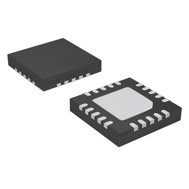
Packaged in a 20pin QFN (4x4)
Applications
•
•
•
•
•
Power load/rail switching
Input supply muxing
Isolated power supplies
Solid state relays
HVAC control
Typical Application Circuit
C2
C1
VDD2
VDD1
CPP
Ccp
SW1
VCC
CISO
CLK
Cdata
DATA
GPIO1
VCC
MCU
VAC
SW2
SUB
TS13001
Final Datasheet
May 14, 2015
Csub
www.semtech.com
Load
GPIO2
SRC
1 of 10
Rev 1.0
Semtech
�Pin Description
Pin #
Pin Name
Pin Function
1
SW2
Switch Output Node 2
2
SW1
Switch Output Node 1
3
SW1
Switch Output Node 1
4
SW2
Switch Output Node 2
5
SW2
Switch Output Node 2
6
SW1
Switch Output Node 1
7
SW1
Switch Output Node 1
8
SW2
Switch Output Node 2
9
SW2
Switch Output Node 2
10
DATA
Data Output
AC Coupled Data Output
11
CLK
Clock Input
AC Coupled Clock and Power Input
12
CPP
Charge Pump Cap
Additional Cap used for lower voltage Clock drive
13
VDD1
Internal Supply 1
Bypass Capacitor for Internal Supply
14
VDD2
Internal Supply 2
Bypass Capacitor for Internal Supply
15
SRC
GND
16
SUB
GND2
17
SW2
Switch Output Node 2
18
SW1
Switch Output Node 1
19
SW1
Switch Output Node 1
20
SW2
Switch Output Node 2
PAD
PAD
Power PAD
TS13001
Final Datasheet
May 14, 2015
Description
Must be floating or connected to SUB
www.semtech.com
2 of 10
Rev 1.0
Semtech
�Functional Block Diagram
VDD1
VDD2
CPP
VDD1
VDD2
CLK
DATA
Digital
Control
SW1
Switch
Driver
Ilimit
Detect
SW2
SUB
SRC
Figure 1: TS13001 Block Diagram
Absolute Maximum Rating
Over operating free–air temperature range unless otherwise noted(1, 2, 3)
Parameter
Range
UNIT
SW1, SW2
-60 to 60
V
CLK, DATA, VDD1, VDD2, CPP
-0.3 to 5.5
V
SUB
-60 to 0.3
V
Operating Junction Temperature Range, TJ
-40 to 125
°C
Storage Temperature Range, TSTG
-65 to 150
°C
±2k
V
+/-200
V
Electrostatic Discharge – IEC Contact (SW1 and SW2 pins)
±8k
V
Electrostatic Discharge – IEC Air Discharge (SW1 and SW2 pins)
±15k
V
Lead Temperature (soldering, 10 seconds)
260
°C
Electrostatic Discharge – Human Body Model
Electrostatic Discharge – Machine Model
Notes:
(1) Stresses beyond those listed under “absolute maximum ratings” may cause permanent damage to the device. These are stress ratings
only and functional operation of the device at these or any other conditions beyond those indicated under “recommended operating
conditions” is not implied. Exposure to absolute–maximum–rated conditions for extended periods may affect device reliability.
(2) All voltage values are with respect to SRC terminal.
(3) ESD testing is performed according to the respective JESD22 JEDEC standard.
TS13001
Final Datasheet
May 14, 2015
www.semtech.com
3 of 10
Rev 1.0
Semtech
�Thermal Characteristics
Electrical Characteristics, TJ = -40C to 125C (unless otherwise noted)
Symbol
Parameter
Value
Units
ΘJA
Thermal Resistance Junction to Air (Note 1)
34.5
°C/W
ΘJC
Thermal Resistance Junction to Case (Note 1)
2.5
°C/W
TSTG
Storage Temperature Range
-65 to 150
°C
Maximum Junction Temperature
150
°C
Operating Junction Temperature Range
-40 to 125
°C
TJ MAX
TJ
Note 1: Assumes 16LD 3x3 QFN with hi-K JEDEC board and 13.5 inch2 of 1 oz Cu and 4 thermal vias connected to PAD
Recommended Operating Conditions
Symbol
Parameter
Min
VSW
AC Switch Voltage
-24
CDATA
Data Isolation Capacitor
100
pF
CISO
Clock Isolation Capacitor
680
pF
CCP
Charge Pump Capacitor
100
pF
CVDD1
CVDD2
VDD1 Bypass Capacitor
10
nF
VDD2 Bypass Capacitor
1
uF
CSUB
Sub Capacitor
100
nF
TS13001
Final Datasheet
May 14, 2015
www.semtech.com
Typ
Max
Unit
24
V
4 of 10
Rev 1.0
Semtech
�Electrical Characteristics
Electrical Characteristics, TJ = -40C to 125C, VCC = 12V (unless otherwise noted)
Symbol
Parameter
Condition
Min
Typ
2.9
15
50
Max
Unit
VCLK Supply Voltage
VCLK
Clock Drive Voltage
5.5
ICLK-NORM
ICLK-NORM
Quiescent current
Normal Mode
VCLK = 5.0V, FCLK = 500KHz
VCLK = 3.0V, FCLK = 1000KHz
ICLK-STBY
Quiescent current
VCLK = 0V
V
uA
uA
3
uA
2000
KHz
VCLK Drive
FCLK
FDATA
NCLKON-INIT
TLOW-ON
NCLKON
Clock Frequency to Turn on Switch
300
Data Frequency during Current
Shutdown
Number of CLK pulses to initialize
Turn On
CLK Low time during Turn On
Sequence
FCLK/4
KHz
3
8
10
20
uS
uS
CLK Pulses to Turn on SW After
TLOW-ON
15
TFASTOFF-INIT
CLK Low time to Initialize Fast TurnOff
10
20
NCLK-FOEN
CLK Pulses to Enable Fast Turn-Off
After TFASTOFF-INIT
6
13
TOFF-FAST
Time for Turn Off
Fast Mode
4
10
uS
TOFF-NORM
Time for Normal Turn Off
Iout < IOFF-TH
60
120
uS
NCLK-OFFDET
CLK Pulses to Detect Incorrect
Turn-On Sequence
Resets with TLOW-ON
RON
On Resistance
Tj=-10C to 65C
75
105
150
mΩ
RON
On Resistance
Tj=25C
90
105
130
mΩ
IOFF
Off State Leakage
3
uA
7.2
A
6.6
A
19
Output Switch
IOUTOC
Output Over Current Shutdown
Tj=-40C to 125C
4.0
IOUTOC
Output Over Current Shutdown
Tj=-10C to 65C
4.4
OCFILT
ITURN-OFF
IOFF-TH
TS13001
Final Datasheet
May 14, 2015
Output Over Current Deglitch
25
Switch Current for Normal Turn-Off
Normal Turn-Off Current Threshold
5.5
-275
Switch will turn off if absolute value
of current is below this threshold after
CLK stops
www.semtech.com
125
200
uS
275
mA
275
mA
5 of 10
Rev 1.0
Semtech
�Application Waveforms
NclkOn-Init
NclkOn
TLow-ON
CLK
Switch State
Figure 2: Clock Turn-on Sequence
TfastOff-Init
NclkFO-EN
TfastOff
Fast
Turn-off
CLK
Switch State
Figure 3: High-speed Turn-off Mode
Toff-Norm & Iout
很抱歉,暂时无法提供与“TS13001-QFNR”相匹配的价格&库存,您可以联系我们找货
免费人工找货