Neo-Iso™
TS13102
Solid State Relay
with Enhanced Diagnostics
TRIUNE PRODUCTS
Features
Description
•
Low Quiescent Operating Currents
2μA in OFF state
5μA in ON state
•
Supports scalable galvanically-isolated I/O
•
Addressable for minimum GPIO usage
Supports eight physical address configurations
•
Single control signal for on/off input (CLK)
Microcontroller-compatible 1.7V to 5.5V input levels
Configurable switching options
•
Switch Characteristics:
Bi-directional blocking in OFF state
Single switch device
60V switch and 290mΩ on-resistance
Up to 2.5A operating current
•
Package Options
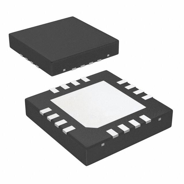
16 lead QFN package – 3x3mm, 1.0mm max height
•
Operating Modes
Zero-cross ON / OFF
Immediate ON / OFF
Dithering Mode for system power sharing
Switch state polling
The TS13102 is a galvanically isolated 60V power
switch device with bi-directional blocking. The
device includes a single integrated 290mΩ high
voltage switch allowing high efficiency switching of
power loads or other high current applications. The
single-pin CLK input pin controls the state of the
switch through sequence options which control the
way the device switches, including immediate on/off,
zero-volt switch-on, zero-current switch-off, dither
modes, as well as latching and non-latching
behavior.
The TS13102 includes several protection features.
Each switch has an integrated over-current shutdown to prevent device damage during short-circuit
or other unusually high load conditions. If an overcurrent event is detected for a time, the switch is
latched off until the CLK turn on sequence is given.
Applications
Summary Specification
•
•
•
Power load / rail switching
Input supply multiplexing
Isolated power supplies
Solid state relays
HVAC control
Sprinkler control
Internet of Things (IoT)
•
•
•
•
•
•
•
Junction operating temperature -40°C to 125°C
Packaged in a 16 pin QFN (3x3)
Product is lead-free, Halogen Free, RoHS / WEEE
compliant
Typical Application Circuit
C VGG
VGG
SRC
C SY S
SYSP
DSW 1
SW1
V AC
AD0
TS13102
LOAD
AD1
VCC
AD2
C ISO
SW2
CLK
DSW 2
μC
C SUB
TS13102
Final Datasheet
28 July 2016
Rev 2.3
SYSM
VDD
WD
CDAT A
SUB
DATA
CVDD
1 of 16
Semtech
Proprietary & Confidential
�Pin Description
Pin Symbol
Pin #
Function
SYSP
1
Positive System Voltage
SYSM
2
Negative System Voltage
SUB
3
IC Substrate Bias
Connect CSUB Capacitor to SYSM
SRC
4
Switch Driver Supply Return
Local common supply return
VGG
5
Internal Switch Driver Supply
Connect Bypass Capacitor CVGG to SRC
SW2
6
Switch Output Node 2
SW2
7
Switch Output Node 2
DATA
8
Data Output
AC Coupled Data Output
CLK
9
Clock Input
AC Coupled Clock Input
WD
10
Watch Dog
Control input for latching vs non-latching Switch
VDD
11
Internal Supply 1
Connect Bypass Capacitor CVDD to SYSM
AD0
12
Address Select 0
AD1
13
Address Select 1
AD2
14
Address Select 2
SW1
15
Switch Output Node 1
SW1
16
Switch Output Node 1
PAD
PAD
Power PAD
Description
Connect CSYS to SYSM
For logic 0, must be tied to SYSM on PCB
For logic 1, must be tied to VDD on PCB
Must be floating or connected to SUB
Functional Block Diagram
Figure 1: TS13102 Block Diagram
TS13102
Final Datasheet
28 July 2016
Rev 2.3
2 of 16
Semtech
Proprietary & Confidential
�Absolute Maximum Ratings
Over operating free–air temperature range unless otherwise noted(1, 4)
Parameter
SW1, SW2
SYSP
(2)
(3)
(3)
CLK , DATA, VDD, AD2, AD1, AD0, WD
Unit
-1 to 60
V
-1 to 60
V
-0.3 to 5.5
V
(2)
-0.3 to 5.5
V
(2)
-55 to 0.3
V
150
°C
-65 to 150
°C
±2k
V
±1.5k
V
260
°C
VGG
SUB
Range
Maximum Junction Temperature, TJ MAX
Storage Temperature Range, TSTG
Electrostatic Discharge – Human Body Model
Electrostatic Discharge – Charged Device Model
Lead Temperature (soldering, 10 seconds)
Notes:
(1)
(2)
(3)
(4)
Stresses beyond those listed under “absolute maximum ratings” may cause permanent damage to the device. These are stress ratings only and
functional operation of the device at these or any other conditions beyond those indicated under “recommended operating conditions” is not implied.
Exposure to absolute–maximum–rated conditions for extended periods may affect device reliability.
Voltage values are with respect to SRC terminal.
Voltage values are with respect to SYSM terminal.
ESD testing is performed according to the respective JESD22 JEDEC standard.
Thermal Characteristics
Symbol
Parameter
θJA
Thermal Resistance Junction to Air (1)
TJ
Operating Junction Temperature Range
Notes:
(1)
Value
Unit
50
°C/W
-40 to 125
°C
Assumes 16 LD 3x3 QFN with hi-K JEDEC board and 13.5 inch2 of 1 oz Cu and 4 thermal vias connected to PAD
TS13102
Final Datasheet
28 July 2016
Rev 2.3
3 of 16
Semtech
Proprietary & Confidential
�Recommended Operating Conditions
Symbol
Parameter
Min
Typ
Max
Unit
24
36
VRMS
60
Hz
VSW
AC Switch Voltage
18
FSYS
System Supply Voltage Frequency
DC
CDATA
Data Isolation Capacitor
100
pF
CISO
Clock Isolation Capacitor
220
pF
CVDD
VDD Bypass Capacitor
470
nF
CVGG
VGG Bypass Capacitor
470
nF
CSUB
Sub Capacitor
100
nF
CWD
Watch Dog Capacitor
22
nF
CSYS
VSYS Capacitor
10
nF
RWD
Watch Dog Resistor
1
MΩ
0.3
V
DSW1/2
SW1/2 Schottky Diode (Forward Voltage)
CLK Drive
VCLK
Clock Drive Voltage
1.7
TCLK
TBIT
TRESET
Clock Period
Bit Period
Reset Time
0.9
7
25
1
8
5.5
V
1.2
10
μs
μs
μs
Electrical Characteristics
Electrical Characteristics, TJ = -40°C to 125°C (unless otherwise noted)
Symbol
Parameter
Condition
Supply and Power Management
Quiescent current
VCLK = 0V, CISO=220pF, FSYS = 60Hz
ICLK-STBY
Disable Mode or Latch Mode
VSW = 24V
ISYSP
System Supply Current
Latch Mode
VDD
VDD Supply Voltage
With respect to SYSM
VGG
VGG Supply Voltage
With respect to SRC
TDOFF
Dither Off Period
TDRTY
Dither Retry Interval
VDON
Dither Voltage ON Threshold
VDOFF
Dither Voltage OFF Threshold
Communication Parameters
THB
Heartbeat Pulse-width
Output Switch
RON
Switch On Resistance
IOFF
Off State Leakage
Output Over Current
IOUTOC
Shutdown
OCFILT
Output Over Current Deglitch
Switch Current for Zero Cross
ITURN-OFF
Turn-Off
Watch Dog
WDTO
Turn-Off Threshold
WDRC
WD Recharge Voltage
TS13102
Final Datasheet
28 July 2016
Rev 2.3
TJ=25°C
TJ
很抱歉,暂时无法提供与“TS13102-QFNR”相匹配的价格&库存,您可以联系我们找货
免费人工找货- 国内价格
- 15+21.68289
- 100+18.70681
- 1000+17.21878
- 国内价格 香港价格
- 1+23.773891+3.07516
- 10+17.6728210+2.28598
- 25+16.1598425+2.09028
- 100+14.49438100+1.87485
- 250+13.69928250+1.77201
- 500+13.38450500+1.73129
- 国内价格 香港价格
- 3300+12.302993300+1.59140
- 6600+12.070896600+1.56137