TVS Diodes
Axial Leaded – 1500W > 1.5KE series
1.5KE Series
RoHS
Pb e3
Description
The 1.5KE Series is designed specifically to protect
sensitive electronic equipment from voltage transients
induced by lightning and other transient voltage events.
Uni-directional
Features
Bi-directional
Agency Approvals
Agency
Agency File Number
E230531
Maximum Ratings and Thermal Characteristics
(TA=25OC unless otherwise noted)
Parameter
Symbol
Value
Unit
PPPM
1500
W
PPPM
2000
W
PD
6.5
W
Peak Forward Surge Current, 8.3ms Single Half
Sine Wave Unidirectional Only (Note 2)
IFSM
200
A
Maximum Instantaneous Forward Voltage at
100A for Unidirectional Only (Note 3)
VF
3.5/5.0
V
Operating Junction and Storage Temperature
Range
TJ , TSTG
-55 to
175
°C
Typical Thermal Resistance Junction to Lead
RθJL
15
°C/W
Typical Thermal Resistance Junction to Ambient
RθJA
75
°C/W
Peak Pulse Power Dissipation (Fig.2) by
10/1000μs Test Waveform (Fig.4) (Note 1)
-Single Die Parts
Peak Pulse Power Dissipation(Fig.2) by
10/1000μs Test Waveform(Fig.4)(Note 1)
-Stacked Die Parts (Note 4)
Steady State Power Dissipation on Infinite Heat
Sink at TL=75ºC
Notes:
1. Non-repetitive current pulse , per Fig. 4 and derated above TJ (initial) =25OC per Fig. 3.
2. Measured on 8.3ms single half sine wave or equivalent square wave, duty cycle=4 per minute maximum.
3. VF < 3.5V for single die parts and VF< 5.0V for stacked-die parts.
4. For stacked die component details, please refer to part numbers labeled by * in Electrical Characteristics.
• 1500W peak pulse
capability at 10/1000μs
waveform, repetition rate
(duty cycles):0.01%
• Glass passivated chip
junction in DO-201
Package
• Fast response time:
typically less than 1.0ps
from 0 Volts to BV min
• Excellent clamping
capability
• �Typical failure mode is
short from over-specified
voltage or current
• �Whisker test is conducted
based on JEDEC
JESD201A per its table 4a
and 4c
• �IEC-61000-4-2 ESD
30kV(Air), 30kV (Contact)
• �ESD protection of data
lines in accordance with
IEC 61000-4-2
• �EFT protection of data
lines in accordance with
IEC 61000-4-4
• Low incremental surge
resistance
• Typical IR less than 1μA
when VBR min>12V
• High temperature
to reflow soldering
guaranteed: 260°C/30sec
/ 0.375”,(9.5mm) lead
length, 5 lbs., (2.3kg)
tension
• �VBR @ TJ= VBR@25°C
x (1+αT x (TJ - 25))
(αT:Temperature
Coefficient, typical value
is 0.1%)
• Plastic package is
flammability rated V-0 per
Underwriters Laboratories
• Matte tin lead–free plated
• Halogen free and RoHS
compliant
• Pb-free E3 means 2nd
level interconnect is
Pb-free and the terminal
finish material is tin(Sn)
(IPC/JEDEC J-STD609A.01)
Applications
TVS devices are ideal for the protection of I/O interfaces,
VCC bus and other vulnerable circuits used in telecom,
computer, industrial and consumer electronic applications.
Additional Infomarion
Functional Diagram
Datasheet
Bi-directional
Cathode
Resources
Samples
Anode
Uni-directional
© 2020 Littelfuse, Inc.
Specifications are subject to change without notice.
Revised: JC.10/30/20
�TVS Diodes
Axial Leaded – 1500W > 1.5KE series
Electrical Characteristics (T =25°C unless otherwise noted)
A
Part
Number
(Uni)
Part
Number
(Bi)
1.5KE6.8A
1.5KE7.5A
1.5KE8.2A
1.5KE9.1A
1.5KE10A
1.5KE11A
1.5KE12A
1.5KE13A
1.5KE15A
1.5KE16A
1.5KE18A
1.5KE20A
1.5KE22A
1.5KE24A
1.5KE27A
1.5KE30A
1.5KE33A
1.5KE36A
1.5KE39A
1.5KE43A
1.5KE47A
1.5KE51A
1.5KE56A
1.5KE62A
1.5KE68A
1.5KE75A
1.5KE82A
1.5KE91A
1.5KE100A
1.5KE110A
1.5KE120A
1.5KE130A
1.5KE150A
1.5KE160A
1.5KE170A
1.5KE180A
1.5KE200A
1.5KE220A
1.5KE250A
1.5KE300A*
1.5KE320A*
1.5KE350A*
1.5KE400A*
1.5KE440A*
1.5KE480A*
1.5KE510A*
1.5KE530A*
1.5KE540A*
1.5KE550A*
1.5KE600A*
1.5KE6.8CA
1.5KE7.5CA
1.5KE8.2CA
1.5KE9.1CA
1.5KE10CA
1.5KE11CA
1.5KE12CA
1.5KE13CA
1.5KE15CA
1.5KE16CA
1.5KE18CA
1.5KE20CA
1.5KE22CA
1.5KE24CA
1.5KE27CA
1.5KE30CA
1.5KE33CA
1.5KE36CA
1.5KE39CA
1.5KE43CA
1.5KE47CA
1.5KE51CA
1.5KE56CA
1.5KE62CA
1.5KE68CA
1.5KE75CA
1.5KE82CA
1.5KE91CA
1.5KE100CA
1.5KE110CA
1.5KE120CA
1.5KE130CA
1.5KE150CA
1.5KE160CA
1.5KE170CA
1.5KE180CA
1.5KE200CA
1.5KE220CA
1.5KE250CA*
1.5KE300CA*
1.5KE320CA*
1.5KE350CA*
1.5KE400CA*
1.5KE440CA*
1.5KE480CA*
1.5KE510CA*
1.5KE530CA*
1.5KE540CA*
1.5KE550CA*
1.5KE600CA*
Reverse Stand Breakdown Voltage VBR
(Volts) @ IT
off Voltage VR
(Volts)
Min.
Max.
5.80
6.45
7.14
6.40
7.13
7.88
7.02
7.79
8.61
7.78
8.65
9.50
8.55
9.50
10.50
9.40
10.50
11.60
10.20
11.40
12.60
11.10
12.40
13.70
12.80
14.30
15.80
13.60
15.20
16.80
15.30
17.10
18.90
17.10
19.00
21.00
18.80
20.90
23.10
20.50
22.80
25.20
23.10
25.70
28.40
25.60
28.50
31.50
28.20
31.40
34.70
30.80
34.20
37.80
33.30
37.10
41.00
36.80
40.90
45.20
40.20
44.70
49.40
43.60
48.50
53.60
47.80
53.20
58.80
53.00
58.90
65.10
58.10
64.60
71.40
64.10
71.30
78.80
70.10
77.90
86.10
77.80
86.50
95.50
85.50
95.00
105.00
94.00
105.00
116.00
102.00
114.00
126.00
111.00
124.00
137.00
128.00
143.00
158.00
136.00
152.00
168.00
145.00
162.00
179.00
154.00
171.00
189.00
171.00
190.00
210.00
185.00
209.00
231.00
214.00
237.00
263.00
214.00
237.00
263.00
256.00
285.00
315.00
273.00
304.00
336.00
300.00
332.00
368.00
342.00
380.00
420.00
376.00
418.00
462.00
408.00
456.00
504.00
434.00
485.00
535.00
451.00
503.50
556.50
460.00
513.00
567.00
468.00
522.50
577.50
512.00
570.00
630.00
Test
Current
IT (mA)
10
10
10
1
1
1
1
1
1
1
1
1
1
1
1
1
1
1
1
1
1
1
1
1
1
1
1
1
1
1
1
1
1
1
1
1
1
1
1
1
1
1
1
1
1
1
1
1
1
1
1
Maximum
Clamping
Voltage
VC @ Ipp
(Volts)
10.5
11.3
12.1
13.4
14.5
15.6
16.7
18.2
21.2
22.5
25.2
27.7
30.6
33.2
37.5
41.4
45.7
49.9
53.9
59.3
64.8
70.1
77.0
85.0
92.0
103.0
113.0
125.0
137.0
152.0
165.0
179.0
207.0
219.0
234.0
246.0
274.0
328.0
344.0
344.0
414.0
441.0
482.0
548.0
602.0
658.0
698.0
725.0
740.0
760.0
828.0
Maximum
Maximum Peak
Reverse
Pulse Current
Leakage IR @ VR
Ipp (A)
(µA)
144.8
134.5
125.6
113.4
104.8
97.4
91.0
83.5
71.7
67.6
60.3
54.9
49.7
45.8
40.5
36.7
33.3
30.5
28.2
25.6
23.5
21.7
19.7
17.9
16.5
14.8
13.5
12.2
11.1
10.0
9.2
8.5
7.3
6.9
6.5
6.2
5.5
4.6
4.4
5.9
4.9
4.6
4.2
3.7
3.1
3.1
2.9
2.8
2.8
2.7
2.5
1000
500
200
50
10
5
5
1
1
1
1
1
1
1
1
1
1
1
1
1
1
1
1
1
1
1
1
1
1
1
1
1
1
1
1
1
1
1
1
1
1
1
1
1
1
1
1
1
1
1
1
Agency
Approval
X
X
X
X
X
X
X
X
X
X
X
X
X
X
X
X
X
X
X
X
X
X
X
X
X
X
X
X
X
X
X
X
X
X
X
X
X
X
X
X
X
X
X
X
X
-
For bidirectional type having VR of 10 volts and less, the IR limit is double.
For parts without A, the VBR is ± 10% and VC is 5% higher than with A parts, the parts without A are currently available, but not recommended for new designs. The parts with A are preferred.
For stack-die parts, use * to label the part number.
© 2020 Littelfuse, Inc.
Specifications are subject to change without notice.
Revised: JC.10/30/20
�TVS Diodes
Axial Leaded – 1500W > 1.5KE series
I-V Curve Characteristics
Uni-directional
Bi-directional
Ipp
Vc VBR VR
IR VF
IT
IT
IR
Vc VBR VR
V
IR
IT
V
Ipp
Ipp
PPPM
VR
VBR
VC
IR
VF
VR VBR Vc
Peak Pulse Power Dissipation -- Max power dissipation
Stand-off Voltage -- Maximum voltage that can be applied to the TVS without operation
Breakdown Voltage -- Maximum voltage that flows though the TVS at a specified test current (IT)
Clamping Voltage -- Peak voltage measured across the TVS at a specified Ippm (peak impulse current)
Reverse Leakage Current -- Current measured at VR
Forward Voltage Drop for Uni-directional
Ratings and Characteristic Curves (T =25°C unless otherwise noted)
A
Figure 1 - TVS Transients Clamping Waveform
Figure 2 - Peak Pulse Power Rating
100
PPPM-Peak Pulse Power (kW)
Voltage Transients
Voltage or Current
Voltage Across TVS
Current Through TVS
TJ initial = Tamb
1
0.1
0.001
Time
stacked-die, 2kW
at 10x1000µs, 25°C
10
Single die, 1.5kW
at 10x1000µs, 25°C
0.01
0.1
1
10
td-Pulse Width (ms)
© 2020 Littelfuse, Inc.
Specifications are subject to change without notice.
Revised: JC.10/30/20
�TVS Diodes
Axial Leaded – 1500W > 1.5KE series
Ratings and Characteristic Curves (T =25°C unless otherwise noted) (Continued)
A
Figure 4 - Pulse Waveform
Figure 3 - Peak Pulse Power Derating Curve
IPPM- Peak Pulse Current, % IRSM
Peak Pulse Power (PPP) or Current (IPP)
Derating in Percentage %
150
100
75
50
25
0
0
25
50
75
100
125
150
175
tr=10µsec
2
50
10/1000µsec. Waveform
as defined by R.E.A
td
1.0
0
2.0
3.0
4.0
Figure 6 - Typical Transient Thermal Impedance
100
Transient Thermal Impedance (°C/W)
100000
Uni-directional V=0V
10000
Bi-directional V=0V
Cj(pF)
( )
t-Time (ms)
Figure 5 - Typical Junction Capacitance
1000
Uni-directional V=VR
100
Bi-directional V=VR
10
1
10
100
10
1
0.1
1000
0.01
VBR - Reverse Breakdown Voltage(V)
0.1
1
10
100
1000
TP - Pulse Duration (s)
Figure 7 - Maximum Non-Repetitive Peak Forward
Surge Current Uni-Directional Only
Figure 8 - Peak Forward Voltage Drop vs Peak Forward
Current (Typical Values)
100.0
200
Single die
180
IF- Peak Forward Current(A)
IFSM - Peak Forward Surge Current (A)
Half Value
IPPM IPPM
0
TJ - Initial Junction Temperature (ºC)
1
Peak Value
IPPM
100
200
TJ=25°C
Pulse Width(td) is defined
as the point where the peak
current decays to 50% of IPPM
160
140
120
100
80
60
40
Stacked-die
10.0
1.0
20
0
1
10
Number of Cycles at 60 Hz
100
0.1
0.0
1.0
2.0
3.0
4.0
5.0
6.0
7.0
8.0
9.0
VF-Peak Forward Voltage(V)
© 2020 Littelfuse, Inc.
Specifications are subject to change without notice.
Revised: JC.10/30/20
�TVS Diodes
Axial Leaded – 1500W > 1.5KE series
Soldering Parameters
Lead–free assembly
Pre Heat
- Temperature Min (Ts(min))
150°C
- Temperature Max (Ts(max))
200°C
- Time (min to max) (ts)
60 – 120 secs
Average ramp up rate (Liquidus Temp (TL) to peak
3°C/second max
TS(max) to TL - Ramp-up Rate
3°C/second max
Reflow
- Temperature (TL) (Liquidus)
217°C
- Time (min to max) (tL)
60 – 150 seconds
Peak Temperature (TP)
260
Time within 5°C of actual peak Temperature (tp)
30 seconds max
Ramp-down Rate
6°C/second max
Time 25°C to peak Temperature (TP)
8 minutes Max.
Do not exceed
260°C
+0/-5
tp
TP
Ramp-up
TL
Temperature (T)
Reflow Condition
tL
Ts(max)
Ts(min)
Ramp-down
ts
Preheat
°C
25˚C
t 25˚C to Peak
Time (t)
Flow/Wave Soldering (Solder Dipping)
Peak Temperature :
265OC
Dipping Time :
10 seconds
Soldering :
1 time
Environmental Specifications
Physical Specifications
Weight
0.045oz., 1.2g
High Temp. Storage
JESD22-A103
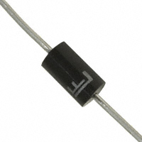
Case
JEDEC DO-201 molded plastic body over passivated junction.
HTRB
JESD22-A108
Polarity
Color band denotes the cathode except Bipolar.
Matte Tin axial leads, solderable per
JESD22-B102.
Temperature Cycling
JESD22-A104
H3TRB
JESD22-A101
RSH
JESD22-B106
Terminal
Critical Zone
TL to TP
Dimensions
D
Cathode Band
Dimensions
(for uni-directional products only)
C
A
B
A
Inches
Millimeters
Min
Max
Min
A
1.000
-
25.40
Max
-
B
0.285
0.375
7.20
9.50
C
0.038
0.042
0.96
1.07
D
0.190
0.210
4.80
5.30
DO-201
© 2020 Littelfuse, Inc.
Specifications are subject to change without notice.
Revised: JC.10/30/20
�TVS Diodes
Axial Leaded – 1500W > 1.5KE series
Part Numbering System
Part Marking System
1.5KE xxx XX X
Cathode Band
Option Code:
Blank Reel Tape
-B Bulk Packaging
F
(for uni-directional
products only)
YYWW
Littelfuse Logo
Type Code:
A Uni-Directional (5% VBR Voltage Tolerance)
CA Bi-Directional (5% VBR Voltage Tolerance)
1.5KEXXX
VBR Voltage Code
(Refer to the Electrical Characteristics table)
Trace Code Marking
YY:Year Code
WW: Week Code
Product Type
Series Code
Packaging
Part Number
Component Package
Quantity
Packaging Option
Packaging Specification
1.5KExxxXX
DO-201
1200
Tape & Reel
EIA STD RS-296
1.5KExxxXX-B
DO-201
500
BULK
Littelfuse Spec.
Tape and Reel Specification
Off Center
either side
0.028(0.7)
2.56
(65.0)
0.236
(6.0)
0.047
(1.2)
0.394+/-0.020
(10.0+/-0.5)
13.0
(330.2)
2.063+0.079/-0.039
(53.0+2.0/-1.0)
Dimensions are in
inches/mm
3.0
(76.2)
0.68
(17.27)
2.75
(69.85)
Recess Depth Max. 0.75 (19.05)
Direction of Feed
Disclaimer Notice - Information furnished is believed to be accurate and reliable. However, users should independently evaluate the suitability of and test each product selected for their own applications. Littelfuse products are
not designed for, and may not be used in, all applications. Read complete Disclaimer Notice at www.littelfuse.com/disclaimer-electronics.
© 2020 Littelfuse, Inc.
Specifications are subject to change without notice.
Revised: JC.10/30/20
�
很抱歉,暂时无法提供与“1.5KE530CA”相匹配的价格&库存,您可以联系我们找货
免费人工找货- 国内价格
- 1+2.07360
- 10+2.01960
- 30+1.99800


 工商网监
湘ICP备2023018690号
工商网监
湘ICP备2023018690号

