TVS Diodes
Surface Mount > 400W > 1SMA10CAT3G Series
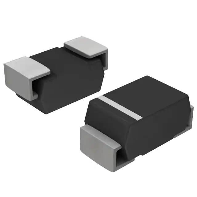
1SMA10CAT3G Series
Pb
Description
The 1SMA10CAT3G series is designed to protect voltage
sensitive components from high voltage, high energy
transients. They have excellent clamping capability, high
surge capability, low zener impedance and fast response
time. The 1SMA10CAT3G series is supplied in the
Littelfuse exclusive, cost-effective, highly reliable package
and is ideally suited for use in communication systems,
automotive, numerical controls, process controls, medical
equipment, business machines, power supplies and many
other industrial/consumer applications.
Features
• Working Peak Reverse Voltage Range − 10 V to 78 V
Maximum Ratings and Thermal Characteristics
• Standard Zener Breakdown Voltage Range −
11.7 V to 91.3 V
Parameter
Symbol
Value
Unit
Peak Power Dissipation (Note 1) @ TL =
25°C, Pulse Width = 1 ms
PPK
400
W
DC Power Dissipation @ TL = 75°C
Measured Zero Lead Length (Note 2)
PD
1.5
W
20
mW/°C
50
°C/W
Derate Above 75°C
Thermal Resistance from Junction−
to−Lead
DC Power Dissipation (Note 3) @ TA =
25°C Derate Above 25°C
Thermal Resistance from Junction–to–
Ambient
R�JL
• Peak Power − 400 W @ 1 ms
• ESD Rating of Class 3 (> 16 kV) per Human Body Model
• Response Time is Typically < 1 ns
• Flat Handling Surface for Accurate Placement
• Package Design for Top Slide or Bottom Circuit
Board Mounting
• Low Profile Package
PD
R0JA
0.5
W
4.0
mW/°C
250
°C/W
• These are Pb−Free Device
Functional Diagram
C
Forward Surge Current (Note 4) @ TA
= 25°C
IFSM
40
A
Operating and Storage Temperature
Range
TJ, Tstg
-65 to
+150
°C
Stresses exceeding those listed in the Maximum Ratings table may damage the device. If
any of these limits are exceeded, device functionality should not be assumed, damage may
occur and reliability may be affected.
Additional Information
Datasheet
Resources
Samples
1. 10 X 1000 µs, non−repetitive.
2. 1” square copper pad, FR−4 board.
3. FR−4 board, using Littelfuse minimum recommended footprint, as shown in 403D-02
case outline dimensions spec.
© 2017 Littelfuse, Inc.
Specifications are subject to change without notice.
Revised: 09/14/17
�TVS Diodes
Surface Mount > 400W > 1SMA10CAT3G Series
I-V Curve Characteristics (T
A
= 25°C unless otherwise noted)
Symbol
IPP
IT
VC VBR VRWM IR
IR VRWM VBR VC
IT
IPP
Parameter
IPP
Maximum Reverse Peak Pulse Current
VC
Clamping Voltage @ IPP
VRWM
Working Peak Reverse Voltage
IR
Maximum Reverse Leakage Current @ VRWM
VBR
Breakdown Voltage @ IT
IT
Test Current
© 2017 Littelfuse, Inc.
Specifications are subject to change without notice.
Revised: 09/14/17
�TVS Diodes
Surface Mount > 400W > 1SMA10CAT3G Series
Electrical Characteristics
VC @ IPP
Breakdown Voltage
Device*
Device
Marking
V
RWM
(Note 6)
IR @
VRWM
Volts
µA
(Note 8)
C Typ.
VBR @ IT (V) (Note 7)
@ IT
VC
IPP
(Note 9)
MIN
NOM
MAX
mA
Volts
Amps
pF
1SMA10CAT3G
QXC
10
2.5
11.1
11.69
12.27
1.0
17.0
23.5
580
1SMA12CAT3G
REC
12
2.5
13.3
14.00
14.70
1.0
19.9
20.1
490
1SMA13CAT3G
RGC
13
2.5
14.4
15.16
15.92
1.0
21.5
18.6
455
1SMA15CAT3G
RMC
15
2.5
16.7
17.58
18.46
1.0
24.4
16.4
400
1SMA16CAT3G
RPC
16
2.5
17.8
18.74
19.67
1.0
26.0
15.4
375
1SMA18CAT3G
RTC
18
2.5
20
21.06
22.11
1.0
29.2
13.7
335
1SMA20CAT3G
RVC
20
2.5
22.2
23.37
24.54
1.0
32.4
12.3
305
1SMA24CAT3G
RZC
24
2.5
26.7
28.11
29.51
1.0
38.9
10.3
260
1SMA26CAT3G
SEC
26
2.5
28.9
30.42
31.94
1.0
42.1
9.5
240
1SMA28CAT3G
SGC
28
2.5
31.1
32.74
34.37
1.0
45.4
8.8
225
1SMA30CAT3G
SKC
30
2.5
33.3
35.06
36.81
1.0
48.4
8.3
210
1SMA33CAT3G
SMC
33
2.5
36.7
38.63
40.56
1.0
53.3
7.5
190
1SMA36CAT3G
SPC
36
2.5
40
42.11
44.21
1.0
58.1
6.9
175
1SMA40CAT3G
SRC
40
2.5
44.4
46.74
49.07
1.0
64.5
6.2
160
1SMA48CAT3G
SXC
48
2.5
53.3
56.11
58.91
1.0
77.4
5.2
135
1SMA58CAT3G
TGC
58
2.5
64.4
67.79
71.18
1.0
93.6
4.3
115
1SMA60CAT3G
TKC
60
2.5
66.7
70.21
73.72
1.0
96.8
4.1
110
1SMA70CAT3G
TPC
70
2.5
77.8
81.90
85.99
1.0
113
3.5
95
1SMA78CAT3G
TTC
78
2.5
86.7
91.27
95.83
1.0
126
3.2
90
1SMA28AT3G
SG
28
2.5
31.1
32.75
34.4
1
45.4
8.8
430
1SMA30AT3G
SK
30
2.5
33.3
35.05
36.8
1
48.4
8.3
405
1SMA33AT3G
SM
33
2.5
36.7
38.65
40.6
1
53.3
7.5
375
1SMA36AT3G
SP
36
2.5
40
42.1
44.2
1
58.1
6.9
345
1SMA40AT3G
SR
40
2.5
44.4
46.75
49.1
1
64.5
6.2
315
1SMA43AT3G
ST
43
2.5
47.8
50.3
52.8
1
69.4
5.8
295
1SMA45AT3G
SV
45
2.5
50
52.65
55.3
1
72.2
5.5
280
1SMA48AT3G
SX
48
2.5
53.3
56.1
58.9
1
77.4
5.2
265
1SMA54AT3G
TE
54
2.5
60
63.15
66.3
1
87.1
4.6
240
1SMA58AT3G
TG
58
2.5
64.4
67.8
71.5
1
93.6
4.3
225
1SMA70AT3G
TP
70
2.5
77.8
81.9
86.0
1
113
3.5
190
1SMA78CAT3G
TTC
78
2.5
86.7
91.27
95.83
1.0
126
3.2
90
4. A transient suppressor is normally selected according to the working peak reverse voltage (VRWM), which should be equal to or greater than
the DC or continuous peak operating voltage level
5. VBR measured at pulse test current IT at an ambient temperature of 25°C
6. Surge current waveform per Figure 2 and derate per Figure 3
7. Bias voltage = 0 V, F = 1.0 MHz, TJ = 25°C.
†Please see 1SMA5.0AT3 to 1SMA78AT3 for Unidirectional devices.
© 2017 Littelfuse, Inc.
Specifications are subject to change without notice.
Revised: 09/14/17
�TVS Diodes
Surface Mount > 400W > 1SMA10CAT3G Series
Ratings and Characteristic Curves
Figure 1. Pulse Rating Curve
Figure 2. Pulse Waveform
Figure 3 - Pulse Derating Curve
Figure 4. Typical Junction Capacitance vs. Bias Voltage
© 2017 Littelfuse, Inc.
Specifications are subject to change without notice.
Revised: 09/14/17
�TVS Diodes
Surface Mount > 400W > 1SMA10CAT3G Series
Dimensions
Soldering Footrpint
HE
4.000
0.157
E
bD D
2.000
0.079
POLARITY INDICATOR
OPTIONAL AS NEEDED
(SEE STYLES)
A
c
L
2.000
0.079
A1
SCALE 8:1
Dim
Inches
mm
inches
Millimeters
Min
Nom
Max
Min
Nom
Max
A
0.078
0.083
0.087
1.97
2.10
2.20
A1
0.002
0.004
0.008
0.05
0.10
0.20
b
0.050
0.057
0.064
1.27
1.45
1.63
c
0.006
0.011
0.016
0.15
0.28
0.41
D
0.090
0.103
0.115
2.29
2.60
2.92
E
0.160
0.170
0.180
4.06
4.32
4.57
HE
0.190
0.205
0.220
4.83
5.21
5.59
L
0.030
0.045
0.060
0.76
1.14
1.52
NOTES:
1. DIMENSIONING AND TOLERANCING PER ANSI Y14.5M, 1982.
2. CONTROLLING DIMENSION: INCH.
ORDERING INFORMATION
Device**
Package
Shipping†
SMA
(Pb−Free)
1SMAxxAT3G
5,000 /
Tape & Reel
**The “T3” suffix refers to a 13 inch reel.
Flow/Wave Soldering (Solder Dipping)
Peak Temperature :
260OC
Dipping Time :
10 seconds
3. DIMENSION b SHALL BE MEASURED WITHIN DIMENSION L.
STYLE 1:
Physical Specifications
PIN 1. CATHODE (POLARITY BAND)
2. ANODE
Case
Void-free, transfer-molded, thermosetting
plastic
Polarity
Cathode indicated by molded polarity
notch
Mounting Position
Any
Finish
All external surfaces are corrosion
resistant and leads are readily solderable
Part Marking System
xxC
AYWW
xxC=
Device Code (Refer to page 3)
A=
Assembly Location
Y=
Year
WW = Work Week
Disclaimer Notice - Information furnished is believed to be accurate and reliable. However, users should independently evaluate the suitability of and
test each product selected for their own applications. Littelfuse products are not designed for, and may not be used in, all applications. Read complete
Disclaimer Notice at: www.littelfuse.com/disclaimer-electronics.
© 2017 Littelfuse, Inc.
Specifications are subject to change without notice.
Revised: 09/14/17
�
很抱歉,暂时无法提供与“1SMA13CAT3G”相匹配的价格&库存,您可以联系我们找货
免费人工找货