Thyristors Datasheet
2N6344
Surface Mount – 600-800V
Pb
Description
The 2N6344 is designed primarily for full-wave AC control applications,
such as light dimmers, motor controls, heating controls and power
supplies; or wherever full-wave silicon gate controlled solid-state
devices are needed. Triac type thyristors switch from a blocking to
a conducting state for either polarity of applied anode voltage with
positive or negative gate triggering.
Features
■ Blocking Voltage to 800 V
■ All Diffused and Glass
Passivated Junctions for
Greater Parameter Uniformity
and Stability
Additional Information
Resources
Accessories
■ Small, Rugged, Thermowatt
Construction for Low Thermal
Resistance, High Heat
Dissipation and Durability
Samples
■ Gate Triggering Guaranteed in
all Four Quadrants
■ For 400 Hz Operation,
Consult Factory
■ Pb−Free Package is Available
Functional Diagram
Pin Out
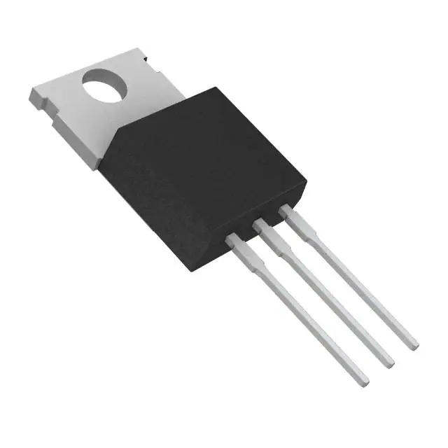
CASE 221A
STYLE 4
1
2
1
© 2021 Littelfuse, Inc.
Specifications are subject to change without notice.
Revised: GD. 02/15/21
�Thyristors Datasheet
2N6344
Surface Mount – 600-800V
Maximum Ratings and Thermal Characteristics (TJ = 25°C unless otherwise noted)
Rating
Symbol
Value
Unit
*Peak Repetitive Off-State Voltage (Note 1)
(TJ = -40 to 110°C, Sine Wave, 50 to 60 Hz, Gate Open)
2N6344
2N6349
VDRM,
VRRM
600
800
V
† On-State RMS Current (TC = +80°C)
Full Cycle Sine Wave 50 to 60 Hz (TC = +90°C)
IT
8.0
4.0
A
ITSM
100
A
I2t
40
A²s
† Peak Non−Repetitive Surge Current
(One Full Cycle, Sine Wave 60 Hz, TC = +25°C) Preceded and followed by rated current
Circuit Fusing Considerations (t = 8.3 ms)
(RMS)
†Peak Gate Power (TC = +80°C, Pulse Width = 2 µs)
PGM
20
W
†Average Gate Power (TC = +80°C, t = 8.3 ms)
PG(AV)
0.5
W
†Peak Gate Current (TC = +80°C, Pulse Width = 2.0 µs)
IGM
2.0
A
†Peak Gate Voltage (TC = +80°C, Pulse Width = 2.0 µs)
VGM
10
V
†Operating Junction Temperature Range
TJ
-40 to +125
°C
Storage Temperature Range
Tstg
-40 to +150
°C
Stresses exceeding Maximum Ratings may damage the device. Maximum Ratings are stress ratings only. Functional operation above the Recommended Operating Conditions is not implied.
Extended exposure to stresses above the Recommended Operating Conditions may affect device reliability.
† Indicates JEDEC Registered Data.
1. VDRM and VRRM for all types can be applied on a continuous basis. Blocking voltages shall not be tested with a constant current source such that the voltage ratings of the devices are exceeded.
Thermal Characteristics
Rating
† Thermal Resistance, Junction to Case
Maximum Lead Temperature for Soldering Purposes, 1/8” from case for 10 seconds
Symbol
Value
Unit
R8JC
2.2
°C/W
TL
260
°C
† Indicates JEDEC Registered Data.
Electrical Characteristics - OFF (TC = 25°C unless otherwise noted; Electricals apply in both
directions)
Characteristic
*Peak Repetitive Blocking Current
(VD = VDRM = VRRM; Gate Open)
TJ = 25°C
TJ = 100°C
2
Symbol
Min
Typ
Max
Unit
IDRM,
IRRM
-
-
10
µA
-
-
2.0
mA
© 2021 Littelfuse, Inc.
Specifications are subject to change without notice.
Revised: GD. 02/15/21
�Thyristors Datasheet
2N6344
Surface Mount – 600-800V
Electrical Characteristics - ON (TC = 25°C unless otherwise noted; Electricals apply in both
directions)
Characteristic
†Peak On−State Voltage
(ITM = ±11 A Peak; Pulse Width = 1 to 2 ms, Duty Cycle ≤ 2%)
Symbol
Min
Typ
Max
Unit
VTM
-
1.3
1.55
V
Gate Trigger Current (Continuous dc) (VD = 12 Vdc, RL = 100 Ω)
Quadrant I: MT2(+), G(+)
Both
-
12
50
Quadrant II: MT2(+), G(−)
2N6349 only
-
12
75
Quadrant III: MT2(−), G(−)
Both
-
20
50
Quadrant IV: MT2(−), G(+)
2N6349 only
-
35
75
IGT
†MT2(+), G(+); MT2(−), G(−) TC = −40°C
-
-
−
100
†MT2(+), G(−); MT2(−), G(+) TC = −40°C
-
-
−
125
Quadrant I: MT2(+), G(+)
Both
−
0.9
2.0
Quadrant II: MT2(+), G(−)
2N6349 only
−
0.9
2.5
Quadrant III: MT2(−), G(−)
Both
−
1.1
2.0
Quadrant IV: MT2(−), G(+)
2N6349 only
−
1.4
2.5
mA
Gate Trigger Voltage (Continuous dc) (VD = 12 Vdc, RL = 100 Ω)
VGT
†MT2(+), G(+); MT2(−), G(−) TC = −40°C
-
−
2.5
†MT2(+), G(−); MT2(−), G(+) TC = −40°C
-
−
3.0
Gate Non−Trigger Voltage (Continuous dc)
(VD = Rated VDRM, RL = 10 k Ω, TJ = 100°C) †MT2(+), G(+); MT2(−), G(−); MT2(+), G(−); MT2(−), G(−)
TC = 25°C
†Holding Current (VD = 12 Vdc, Gate Open) TC = 25°C
(Initiating Current = 200 mA) *TC = −40°C
TC = -40°C
†Turn-On Time (VD = Rated VDRM, ITM = 11 A, IGT = 120 mA, Rise Time = 0.1 µs, Pulse Width = 2 µs)
VGD
IH
tgt
0.2
-
-
-
6.0
40
-
-
75
-
8
10
V
V
mA
µs
†Indicates JEDEC Registered Data.
Dynamic Characteristics
Characteristic
Symbol
Min
Typ
Max
Unit
Critical Rate of Rise of Commutation Voltage (VD = Rated VDRM, ITM = 11 A, Commutating di/
dt = 4.0 A/ms, Gate Unenergized, TC = 80°C)
dv/dt(c)
−
5.0
−
V/µs
Voltage Current Characteristic of Triacs (Bidirectional Device)
Symbol
Parameter
VDRM
Peak Repetitive Forward Off State Voltage
IDRM
Peak Forward Blocking Current
VRRM
Peak Repetitive Reverse Off State Voltage
IRRM
Peak Reverse Blocking Current
VTM
Maximum On State Voltage
IH
Holding Current
I
I
I
3
I
© 2021 Littelfuse, Inc.
Specifications are subject to change without notice.
Revised: GD. 02/15/21
�Thyristors Datasheet
2N6344
Surface Mount – 600-800V
Quadrant Definitions for a Triac
Q u a dr a n t II
Q ua dr a nt I
I
Q u a dr a n t III
Q u a dr a n t IV
All polarities are referenced to MT1.
With in−phase signals (using standard AC lines) quadrants I and III are used.
Ratings and Characteristic Curves
Figure 1. RMS Current Derating
Figure 2. On−State Power Dissipation
4
© 2021 Littelfuse, Inc.
Specifications are subject to change without notice.
Revised: GD. 02/15/21
�Thyristors Datasheet
2N6344
Surface Mount – 600-800V
Figure 3. Typical Gate Trigger Voltage
Figure 4. Typical Gate Trigger Current
Figure 7. Maximum On-State Characteristics
Figure 8. Typical Holding Current
Figure 9. Maximum Allowable Surge Current
5
© 2021 Littelfuse, Inc.
Specifications are subject to change without notice.
Revised: GD. 02/15/21
�Thyristors Datasheet
2N6344
Surface Mount – 600-800V
Figure 10. Thermal Response
Dimensions
B
F
4
Q
12
T
C
S
A
U
3
H
K
Z
R
L
V
J
G
D
N
Part Marking System
CASE 221A
STYLE 4
1
2
Inches
Dim
SEATIN
PLANE
2N6344G
YMAXX
Y =Year
M =Month
A =Assembly Site
XX =Lot Serial Code
G =Pb-Free Package
Device
Package
TO-220AB
2N6344G
TO-220AB
(Pb-Free)
Max
Min
Max
A
0.590
0.620
14.99
15.75
B
0.380
0.420
9.65
10.67
C
0.178
0.188
4.52
4.78
D
0.025
0.035
0.64
0.89
F
0.142
0.147
3.61
3.73
G
0.095
0.105
2.41
2.67
H
0.110
0.130
2.79
3.30
J
0.018
0.024
0.46
0.61
K
0.540
0.575
13.72
14.61
L
0.060
0.075
1.52
1.91
N
0.195
0.205
4.95
5.21
Q
0.105
0.115
2.67
2.92
R
0.085
0.095
2.16
2.41
S
0.045
0.060
1.14
1.52
T
0.235
0.255
5.97
6.47
U
0.000
0.050
0.00
1.27
V
0.045
-
1.15
-
Z
-
0.080
-
2.04
1. Dimensioning And Tolerancing Per Ansi Y14.5m, 1982.
2. Controlling Dimension: Inch.
3. Dimension Z Defines A Zone Where All Body And Lead Irregularities Are Allowed.
Pin Assignment
Ordering Information
2N6344
G
Millimeters
Min
Shipping†
1
Main Terminal 1
2
Main Terminal 2
3
Gate
4
Main Terminal 2
1000 Units / Box
Disclaimer Notice - Information furnished is believed to be accurate and reliable. However, users should independently evaluate the suitability of and test each product selected for their own applications. Littelfuse products are
not designed for, and may not be used in, all applications. Read complete Disclaimer Notice at: www.littelfuse.com/disclaimer-electronics.
© 2021 Littelfuse, Inc.
6
Specifications are subject to change without notice.
Revised: GD. 02/15/21
�