Thyristors
Surface Mount – 600V - 800V > MAC4DSM, MAC4DSN
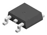
MAC4DSM, MAC4DSN
Pb
Description
The MAC4DSM and MAC4DSN are designed for high
volume, low cost, industrial and consumer applications
such as motor control; process control; temperature, light
and speed control.
Features
• Small Size Surface Mount
DPAK Package
• Passivated Die for
Reliability and Uniformity
• Blocking Voltage to 800 V
• On−State Current Rating
of 4.0 A RMS at 108°C
• Low IGT − 10 mA
Maximum in 3 Quadrants
• High Immunity to dv/dt −
50 V/μs at 125°C
• Epoxy Meets UL 94 V−0
@ 0.125 in
• ESD Ratings: Human
Body Model, 3B > 8000 V
Machine Model, C > 400
V
• Pb−Free Packages are
Available
Functional Diagram
Pin Out
MT 2
4
MT 1
G
TO-220AB
Case 221 A
Style 4
1
2
3
© 2020 Littelfuse, Inc.
Specifications are subject to change without notice.
Revised: BA.09/02/20
�Thyristors
Surface Mount – 600V - 800V > MAC4DSM, MAC4DSN
Maximum Ratings (TJ = 25°C unless otherwise noted)
Rating
Symbol
Value
Unit
VDRM,
VRRM
600
800
V
IT
4.0
A
MAC4DSM
MAC4DSN
Peak Repetitive Off-State Voltage (Note 1)
(Gate Open, Sine Wave 50 to 60 Hz, TJ = -40° to 110°C)
On-State RMS Current (Full Cycle Sine Wave, 60 Hz, TC = 108°C)
(RMS)
Peak Non-Repetitive Surge Current
(One Full Cycle Sine Wave, 60 Hz, TC= 108°C)
ITSM
40
A
Circuit Fusing Consideration (t = 8.3 msec)
2
It
6.6
A²sec
Peak Gate Current (Pulse Width ≤ 20 µsec, TC= 108°C)
IGM
4.0
A
Peak Gate Power (Pulse Width ≤ 10 µsec, TC= 108°C)
PGM
2.0
W
Peak Gate Voltage (Pulse Width ≤ 20 µsec, TC= 108°C)
VGM
5.0
V
Average Gate Power (t = 8.3 msec, TC= 108°C)
PG(AV)
1.0
W
Operating Junction Temperature Range
TJ
-40 to +125
°C
Storage Temperature Range
Tstg
-40 to +150
°C
Stresses exceeding Maximum Ratings may damage the device. Maximum Ratings are stress ratings only. Functional operation above the Recommended Operating Conditions is not implied. Extended exposure to stresses above the
Recommended Operating Conditions may affect device reliability.
1. VDRM and VRRM for all types can be applied on a continuous basis. Ratings apply for zero or negative gate voltage; however, positive gate voltage shall not be applied concurrent with negative potential on the anode. Blocking voltages
shall not be tested with a constant current source such that the voltage ratings of the devices are exceeded.
Thermal Characteristics
Rating
Junction−to−Case (AC)
Junction−to−Ambient
Junction−to−Ambient (Note 2)
Thermal Resistance
Maximum Lead Temperature for Soldering Purposes, 1/8” from case for
10 seconds (Note 3)
Symbol
Value
Unit
RƟJC
RƟJA
RƟJA
3.5
88
80
°C/W
TL
260
°C
2. These ratings are applicable when surface mounted on the minimum pad sizes recommended.
3. 1/8" from case for 10 seconds.
Electrical Characteristics - OFF (TJ = 25°C unless otherwise noted ; Electricals apply in both directions)
Characteristic
TJ = 25°C
TJ = 125°C
Peak Repetitive Blocking Current
(VD = VDRM = VRRM; Gate Open)
Symbol
Min
Typ
Max
IDRM,
IRRM
-
-
0.01
-
-
2.0
Unit
mA
Electrical Characteristics - ON (TJ = 25°C unless otherwise noted; Electricals apply in both directions)
Characteristic
Symbol
Peak On−State Voltage (Note 4) (ITM = ±6.0 A)
Gate Trigger Current
(Continuous dc)
(VD = 12 V, RL = 100 Ω)
VTM
Unit
V
1.3
1.6
4.0
10
2.9
5.0
10
2.9
7.0
10
2.0
5.5
1.5
_
6.0
30
_
10
30
_
6.0
30
0.5
0.7
1.3
0.5
0.65
1.3
MT2(−), G(−)
0.5
0.7
1.3
MT2(+), G(+)
0.2
0.4
−
0.2
0.4
−
0.2
0.4
−
MT2(+), G(−)
IGT
MT2(−), G(−)
IH
MT2(+), G(−)
IL
MT2(−), G(−)
Gate Non−Trigger Voltage
(TJ = 125°C)
(VD = 12 V, RL = 100 Ω)
Max
−
MT2(+), G(+)
Gate Trigger Voltage
(Continuous dc)
(VD = 12 V, RL = 100 Ω)
Typ
2.9
MT2(+), G(+)
Holding Current (VD = 12 V, Gate Open, Initiating Current = ±200 mA))
Latching Current
Min
MT2(+), G(+)
MT2(+), G(−)
MT2(+), G(−)
MT2(−), G(−)
VGT
VGD
mA
mA
mA
V
V
4. Indicates Pulse Test: Pulse Width ≤ 2.0 ms, Duty Cycle ≤ 2%.
© 2020 Littelfuse, Inc.
Specifications are subject to change without notice.
Revised: BA.09/02/20
�Thyristors
Surface Mount – 600V - 800V > MAC4DSM, MAC4DSN
Dynamic Characteristics
Characteristic
Rate of Change of Commutating Current
(VD = 400 V, ITM = 3.5 A, Commutating dv/dt = 10 V/µsec, Gate Open,
TJ = 125°C, f = 500 Hz, CL = 5.0 µF, LL = 20 mH, No Snubber) See Figure 16
Critical Rate of Rise of Off-State Voltage
(VD = 0.67 x VDRM, Exponential Waveform, Gate Open, TJ = 125°C)
Symbol
Min
Typ
Max
Unit
(dI/dt)c
3.0
4.0
−
A/ms
dV/dt
50
175
−
V/µs
Voltage Current Characteristic of SCR
Symbol
VDRM
Peak Repetitive Forward Off State Voltage
IDRM
Peak Forward Blocking Current
VRRM
Peak Repetitive Reverse Off State Voltage
IRRM
Peak Reverse Blocking Current
VTM
Maximum On State Voltage
IH
+Current
Parameter
VTM
On State
IRRM at VRRM
Holding Current
IH
Quadrant 3
Main Terminal 2-
Quadrant Definitions for a Triac
Quadrant 1
Main Terminal 2+
IH
Off State
+Voltage
IDRM at VDRM
VTM
MT2 Positive
(Positive Half Cycle)
+
(+) MT 2
Quadrant II
(-) IGT
Gate
(+) MT 2
(-) IGT
Gate
Quadrant I
MT 1
MT 1
REF
REF
(-) MT 2
(-) MT 2
IGT
Quadrant III
+
(-) IGT
Gate
(-) IGT
Gate
Quadrant IV
MT 1
REF
IGT
MT 1
REF
MT2 Negative
(Negative Half Cycle)
All Polarities are referenced to MT1.
With in-phase signals (using standard AC lines) quadrants I and III are used
© 2020 Littelfuse, Inc.
Specifications are subject to change without notice.
Revised: BA.09/02/20
�Thyristors
Surface Mount – 600V - 800V > MAC4DSM, MAC4DSN
Figure 3. On−State Characteristics
Figure 4. Transient Thermal Response
100
TYPICAL @ TJ = 25°C
MAXIMUM @ JT= 125°C
10
MAXIMUM @ JT= 25°C
1.0
0.1
0
.
10
.
20
.
30
4.0
5.0
VT, INSTANTANEOUS ON-STATE VOLTAGE (VOLTS)
Figure 5. Typical Gate Trigger Current vs, Junction Temperature
r(t), TRANSIEN T RESIST ANCE (NORMALIZED)
Figure 2. On-State Power Dissipation
IT, INSTANTANEOUS ON-STATE CURRENT (AMPS)
Figure 1. Typical RMS Current Derating
1.0
0.1
Z JC(t) = R JC(t) r(t)
0.01
0.1
1.0
10
100
1000
10 K
t, TIME (ms)
Figure 6. Typical Gate Trigger Voltage vs. Junction Temperature
© 2020 Littelfuse, Inc.
Specifications are subject to change without notice.
Revised: BA.09/02/20
�Thyristors
Surface Mount – 600V - 800V > MAC4DSM, MAC4DSN
Figure 7. Typical Holding Current vs. Junction Temperature
Figure 8. Typical Latching Current vs.Junction Temperature
25
Q2
12
10
IL, LATCHING CURRENT (mA)
IH , HOLDING CURRENT (mA)
14
MT2 NEGATIVE
8.0
6.0
MT2 POSITIVE
4.0
2.0
-
0
-50
25
0
25
50
75
Q3
10
5.0
-
TJ , JUNCTION TEMPERA TURE (°C)
Figure 9. Exponential Static dv/dt vs.
Gate−MT1 Resistance, MT2(+)
25
50
75
100
125
STATIC dv/dt (V/ s)
600
VPK = 400V
400
600V
200
800
600
400
200
800V
0
100
1000
TJ = 125°C
VPK = 400V
1000
800
600V
800V
0
10 k
1000
100
R G-MT1, GATE-MT1 RESIST ANCE (OHMS)
10 k
R G-MT1, GATE-MT1 RESIST ANCE (OHMS)
Figure 9. Exponential Static dv/dt vs.
Gate−MT1 Resistance, MT2(+)
Figure 10. Exponential Static dv/dt vs.
Gate−MT1 Resistance, MT2(-)
2000
800
GATE OPEN
TJ = 100°C
400
GATE OPEN
1600
600
STATIC dv/dt (V/ s)
STATIC dv/dt (V/ s)
25
1200
TJ = 125°C
110°C
125°C
200
0
0
TJ , JUNCTION TEMPERA TURE (°C)
Figure 10. Exponential Static dv/dt vs.
Gate−MT1 Resistance, MT2(-)
1000
STATIC dv/dt (V/ s)
Q1
15
0
-50
125
100
20
TJ = 100°C
1200
110°C
800
125°C
400
400
500
600
VPK, PEAK VOLTAGE (VOLTS)
700
800
0
400
500
600
700
800
VPK, PEAK VOLTAGE (VOLTS)
© 2020 Littelfuse, Inc.
Specifications are subject to change without notice.
Revised: BA.09/02/20
�Thyristors
Surface Mount – 600V - 800V > MAC4DSM, MAC4DSN
Figure 13. Typical Holding Current vs. Junction Temperature
Figure 14. Typical Latching Current vs.Junction Temperature
800
1600
VPK = 400V
600
400
600V
200
VPK = 400V
1200
1000
800
600V
600
400
800V
0
GATE OPEN
1400
STATIC dv/dt (V/ s)
STATIC dv/dt (V/ s)
GATE OPEN
100
200
105
110
125
120
115
0
800V
100
105
110
115
120
125
TJ , JUNCTION TEMPERA TURE (°C)
TJ , JUNCTION TEMPERA TURE (°C)
Figure 15. Typical Holding Current vs. Junction Temperature
dv/dt(c), CRITICAL RATE OF RISE OF
COMMUTATING VOLTAGE (V/ s)
100
VPK = 400V
TJ = 125°C
100°C
75°C
10
tw
VDRM
1.0
0
f=
1
2 tw
(di/dt)
c=
6fITM
1000
.
10
50
15
20
di/dt(c), RATE OF CHANGE OF COMMUTATING CURRENT (A/ms)
Figure 16. Simplified Test Circuit to Measure the Critical Rate of Rise of Commutating Current (di/dt)
LL
200VRMS
ADJUST FOR
TM, 60 Hz VAC
1N4007
CHARGE
TRIGGER
CHARGE
CONTROL
CL
TRIGGER CONTROL
MEASURE
I
-
+
200V
MT2
1N914 51
G
MT1
Note: Component values are for verification of rated (di/d
t)c. See AN1048 for additional informatio
n.
© 2020 Littelfuse, Inc.
Specifications are subject to change without notice.
Revised: BA.09/02/20
�Thyristors
Surface Mount – 600V - 800V > MAC4DSM, MAC4DSN
Dimensions
Soldering Footprint
A
E
b3
c2
4
L3
D
12
L4
6.20
0.244
C
A
B
b2
Z
Detail A
NOTE 7
e
Top View
5.80
0.228
c
Bottom View
Side View
b
0.005 (0).13
M
Z
H
3
C
6.17
0.243
Alternate
Construction
SCALE 3: 1
C Seating
Plane
L
1.60
0.063
Bottom View
H
GAUGE
PLANE
L2
2.58
0.102
3.00
0.118
mm
inches
A1
L1
Detail A
Rotated 90°C W
Dim
Inches
Millimeters
Min
Max
Min
Max
A
0.087
0.094
2.20
2.40
A1
0.000
0.005
0.00
0.12
b
0.022
0.030
0.55
0.75
b2
0.026
0.033
0.65
0.85
b3
0.209
0.217
5.30
5.50
c
0.019
0.023
0.49
0.59
c2
0.019
0.023
0.49
0.59
D
0.213
0.224
5.40
5.70
E
0.252
0.260
6.40
6.60
0.091
e
2.30
H
0.374
0.406
9.50
L
0.058
0.070
1.47
0.114
L1
10.30
1.78
2.90
L2
0.019
0.023
0.49
L3
0.053
0.065
1.35
0.59
1.65
L4
0.028
0.039
0.70
1.00
Z
0.154
-
3.90
-
1. Dimensioning and tolerancing per ansi y14.5m, 1982.
2. Controlling Dimension: inch. Style 6: Pin 1. Mt1
2. Mt2
3. Gate
4. Mt2
© 2020 Littelfuse, Inc.
Specifications are subject to change without notice.
Revised: BA.09/02/20
�Thyristors
Surface Mount – 600V - 800V > MAC4DSM, MAC4DSN
Dimensions
Part Marking System
4
DPAK-3
Case 369D
1 2
TO251-3L POD
B
R
4
E
V
A
1
N
F
SEATING
PLANE
DPAK-3
Case 369D
Style 6
Z
-T-
2
3
F
K
G
J
G
D
3PL
0.13 (0.0005)
H
Dim
Inches
Max
Min
Max
A
0.213
0.224
5.40
5.70
B
0.252
0.260
6.40
6.60
C
0.087
0.094
2.20
2.40
D
0.024
0.030
0.60
0.75
E
0.022
0.026
0.55
0.65
F
0.022
0.03
0.58
0.091
0.046
0.050
1.18
1.28
0.019
0.023
0.49
0.59
K
0.291
0.315
7.40
8.00
N
0.03
0.038
0.78
0.98
R
0.209
0.217
5.30
5.50
0.065
1.35
0.063
Z
0.053
T
Pin Assignment
1
Main Terminal 1
2
Main Terminal 2
3
Gate
4
Main Terminal 2
0.78
J
S
=Device Code
=M, or N
=Year
=Month
=Assembly Site
=Lot Serial Code
=Pb-Free Package
2.30
H
V
AC4DCx
x
Y
M
A
XX
G
AC
4DSxG
YMAXX
Millimeters
Min
G
AC
4DSxG
YMAXX
3
C
S
DPAK-3
Case 369C
Style 6
1.60
0.150
1. Dimensioning and Tolerancing Per ANSI Y14.5M, 1982.
2. Controlling Dimension: Inch.
STYLE 6:Pin 1. MT1
2. MT2
3. Gate
4. MT2
Ordering Information
Device
Package Type
Package
Shipping
MAC4DSM−001
DPAK−3
369D
4000 Unit/Box
MAC4DSM−001G
DPAK−3
(Pb−Free)
369D
4000 Unit/Box
MAC4DSMT4
DPAK−3
369C
2500 / Tape & Reel
MAC4DSMT4G
DPAK−3
(Pb−Free)
369C
2500 / Tape & Reel
MAC4DSN−001
DPAK−3
369D
4000 Unit/Box
MAC4DSN−001G
DPAK−3
(Pb−Free)
369D
4000 Unit/Box
MAC4DSNT4
DPAK−3
369C
2500 / Tape & Reel
1.65
3.80
Disclaimer Notice - Information furnished is believed to be accurate and reliable. However, users should independently evaluate the suitability of and test each product selected for their own applications. Littelfuse products are
not designed for, and may not be used in, all applications. Read complete Disclaimer Notice at: www.littelfuse.com/disclaimer-electronics
© 2020 Littelfuse, Inc.
Specifications are subject to change without notice.
Revised: BA.09/02/20
�