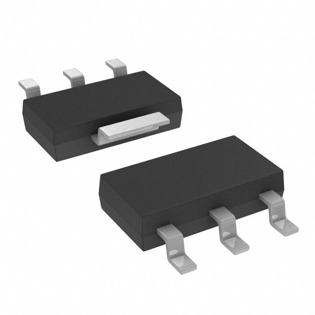
Thyristor Datasheet
MCR08B, MCR08M
Surface Mount – 600V - 800V
RoHS
Pb
Description
PNPN devices designed for line powered consumer applications
such as relay and lamp drivers, small motor controls, gate drivers
for larger thyristors, and sensing and detection circuits. Supplied in
surface mount package for use in automated manufacturing.
Features
■ Sensitive Gate Trigger Current
■ Surface Mount Package
■ Blocking Voltage to 600 V
■ Lead-free and RoHScompliant
■ Glass Passivated Surface for
Reliability and Uniformity
Functional Diagram
G
Additional Information
A
K
Pin Out
4
Resources
Accessories
Samples
1
1
2
3
© 2021 Littelfuse, Inc.
Specifications are subject to change without notice.
Revised: TK. 09/04/21
�Thyristor Datasheet
MCR08B, MCR08M
Surface Mount – 600V - 800V
Maximum Ratings (TJ = 25 °C unless otherwise noted)
Rating
Symbol
Value
VDRM,
VRRM
IT (RMS)
200
600
0.8
A
ITSM
8.0
A
I2t
0.4
A²sec
W
MCR08B
MCR08M
Peak Repetitive Off−State Voltage (Note 1)
(Sine Wave, RGK=1 kΩ TJ = 25 to 110°C)
On-State RMS Current (All Conduction Angles; TC = 80°C)
Peak Non-Repetitive Surge Current
(1/2 Cycle Sine Wave, 60 Hz, TC = 25°C)
Circuit Fusing Consideration (t = 8.3 ms)
Forward Peak Gate Power (TC = 80°C, t = 1.0 µs)
Unit
V
PGM
0.1
PGM (AV)
0.01
W
Operating Junction Temperature Range
TJ
-40 to +110
°C
Storage Temperature Range
Tstg
-40 to +150
°C
Average Gate Power (t = 8.3 ms, TC = 80°C)
Thermal Characteristics
Rating
Symbol
Value
Unit
Thermal Resistance, JJunction−to−Ambient PCB Mounted per Figure 1
RθJA
156
°C/W
Thermal Resistance, Junction−to−Tab Measured on Anode Tab Adjacent to Epoxy
RθJA
25
°C/W
Maximum Device Temperature for Soldering Purposes (for 10 Seconds Maximum)
TL
260
°C
Stresses exceeding Maximum Ratings may damage the device. Maximum Ratings are stress ratings only. Functional operation above the Recommended Operating Conditions is not implied. Extended exposure to stresses above the
Recommended Operating Conditions may affect device reliability.
1. VDRM and VRRM for all types can be applied on a continuous basis. Ratings apply for zero or negative gate voltage; however, positive gate voltage shall not be applied concurrent with negative potential on the anode. Blocking voltages
shall not be tested with a constant current source such that the voltage ratings of the devices are exceeded.
Electrical Characteristics - OFF (TJ = 25°C unless otherwise noted ; Electricals apply in both directions)
Characteristic
Peak Repetitive Forward or Reverse Blocking Current (Note 3)
(VAK = Rated VDRM or VRRM, RGK = 1 kΩ
Symbol
Min
Typ
IDRM
IRRM
-
TJ = 25°C
TJ = 110°C
Max
Unit
-
10
μA
-
200
μA
Electrical Characteristics - ON (TJ = 25°C unless otherwise noted; Electricals apply in both directions)
Characteristic
Symbol
Min
Typ
Peak Forward On-State Voltage (Note 2) (IT = 1.0 A Peak)
VTM
−
−
1.7
V
Gate Trigger Current (Continuous dc) (Note 4) (VAK = 12 Vdc, RL = 100 Ω)
IGT
−
−
200
μA
mA
Holding Current (Note 3) (VAK = 12 Vdc, Initiating Current = 20 mA)
Max
Unit
IH
−
−
5.0
Gate Trigger Voltage (Continuous dc) (VD = 12 V, RL = 100 Ω)
VGT
−
−
0.8
V
Turn−On Time (VAK = 12 Vdc, ITM = 5 Adc, IGT = 5 mA)
tgt
−
1.25
−
µs
2. Pulse Test: Pulse Width ≤ 300 µs, Duty Cycle ≤ 2%.
3. RGK = 1000 Q is included in measurement.
4. RGK is not included in measurement.
Dynamic Characteristics
Characteristic
Critical Rate-of-Rise of Off State Voltage
(Vpk = Rated VDRM, TC = 110°C, RGK = 1 kΩ, Exponential Method)
2
Symbol
Min
Typ
Max
Unit
dv/dt
10
−
−
V/µs
© 2021 Littelfuse, Inc.
Specifications are subject to change without notice.
Revised: TK. 09/04/21
�Thyristor Datasheet
MCR08B, MCR08M
Surface Mount – 600V - 800V
Voltage Current Characteristic of SCR
+Current
Symbol
Parameter
VDRM
Peak Repetitive Forward Off State Voltage
IDRM
Peak Forward Blocking Current
VRRM
Peak Repetitive Reverse Off State Voltage
IRRM
Peak Reverse Blocking Current
VTM
Maximum On State Voltage
IH
Holding Current
Anode+
VTM
on state
IRRM at VRRM
Forward Blocking Region
(Off State)
Reverse Avalanche Region
Anode-
IH
+Voltage
IDRM at VDRM
Forward Blocking Region
(Off State)
Figure 1.
PCB for Thermal Impedance and Power Testing of SOT-223
0.15
3.8
0.079
2.0
0.091 0.091
2.3
2.3
0.079
2.0
0.984
25.0
0.059 0.059
1.5
1.5
0.059
1.5
0.096
2.44
0.096
2.44
0.059
1.5
0.244
6.2
inches
mm
0.096
2.44
0.059
1.5
0.472
12.0
Board mounted vertically cinch 8840 edge connector.
Board Thickness = 65Mil.
Foil Thickness = 2.5Mil.
Material: G10 Fiberglass Base Epoxy
3
© 2021 Littelfuse, Inc.
Specifications are subject to change without notice.
Revised: TK. 09/04/21
�Thyristor Datasheet
MCR08B, MCR08M
Surface Mount – 600V - 800V
Figure 3.
Junction to Ambient Thermal Resistance
vs Copper Tab Area
10
0.1
0.01
TYPICAL AT TJ = 110 C
MAX AT TJ = 110 C
MAX AT TJ = 25 C
0
150
140
130
120
110
100
90
80
70
60
50
40
30
R�JA, Junction to Ambient
Thermal Resistance (°C)
1
1.0
2.0
3.0
4.0
VT, Instantaneous On-state Voltage (V)
1.0 2.0 3.0 4.0 5.0 6.0 7.0 8.0 9.0 10
Foil Area (cm2)
Figure 5.
Current Derating, 1.0 cm Square Pad Reference:
Ambient Temperature
110
100
90
110
100
90
80
70
60
50
40
30
20
50 or 60 Hz Halfwave
α
α = CONDUCTION
ANGLE
dc
180°
120°
α = 30°
60°
0
90°
0.1
0.2
0.3
0.4
IT(AV), Average On-state Current (A)
0.5
80
70
60
50
40
30
20
Figure 6.
Current Derating, 2.0 cm Square Pad Reference:
Ambient Temperature
dc
100
80
60°
70
90°
60
50
120°
α = 30°
α
α = CONDUCTION
ANGLE
0
0.1
0.2
0.3
0.4
IT(AV), Average On-state Current (A)
1.0 cm2 Foil,
50 or 60 Hz Halfwave
180°
120°
α = 30°
60°
90°
α
α = CONDUCTION
ANGLE
0
0.1
0.2
0.3
0.4
IT(AV), Average On-state Current (A)
110
Pad Area = 4.0 cm2
50 or 60 Hz Halfwave
180°
90
dc
0.5
Figure 7.
Current Derating Reference: Anode Tab
TA, Maximum Allowable
Ambient Temperature (°C)
110
TA, Maximum Allowable
Ambient Temperature (°C)
0
Figure 4.
Current Derating, Minimum Pad Size Reference:
Ambient Temperature
TA, Maximum Allowable
Ambient Temperature (°C)
TA, Maximum Allowable
Ambient Temperature (°C)
IT, Instantaneous On-state Current (A)
Figure 2.
On-State Characteristics
4
50 or 60 Hz Halfwave
180°
120°
� = 30°
60°
α
90°
��= CONDUCTION
85
0.5
dc
ANGLE
0
0.1
0.2
0.3
0.4
IT(AV), Average On-state Current (A)
0.5
© 2021 Littelfuse, Inc.
Specifications are subject to change without notice.
Revised: TK. 09/04/21
�Thyristor Datasheet
MCR08B, MCR08M
Surface Mount – 600V - 800V
1.0
0.9
0.8
0.7
0.6
0.5
0.4
0.3
0.2
0.1
0
Figure 9.
Thermal Response Device Mounted on Figure 1 Printed
Circuit Board
1.0
�
��= CONDUCTION
ANGLE
� = 30°
rT, Normalized Transient
Thermal Resistance
P(AV), Maximum Average
Power Dissipatiion (W)
Figure 8.
Power Dissipation
60°
90°
dc
180°
120°
0
0.1
0.2
0.3
0.4
IT(AV), Average On-state Current (A)
0.01
0.0001
0.5
0.7
VAK = 12 V
R L = 100 �
0.5
0.4
0.3
-40
-20
0
20
40
60
80
TJ, Junction Temperature (oC)
110
Figure 12.
Typical Range of VGT versus Measured IGT
0
10
100
2.0
VAK = 12 V
RL = 3.0 k
1.0
0
-40
-20
0
20
40
60
80
TJ, Junction Temperature (oC)
110
1000
IGT, Gate Trigger Current (µA)
VGT, Gate Trigger Voltage (V)
0.011
0.1
t, Time (Seconds)
Figure 13.
Typical Gate Trigger Current vs Junction Temperature
0.7
0.65
0.6
0.55
0.5
VAK = 12 V
R L = 100 �
TJ = 25�C
0.45
0.4
0.35
0.3
0.001
Figure 11.
Typical Normalized Holding Current vs Junction Temperature
IH, Holding Current (Normalized)
VGT, Gate Trigger Voltage (V)
Figure 10.
Typical Gate Trigger Voltage vs Junction Temperature
0.6
0.1
0.1
1.0
10
100
IGT, Gate Trigger Current (µA)
1000
5
RGK = 1000 ��
Resistor Current Included
100
Without Gate Resistor
1.0
-40
-20
VAK = 12 V
RL = 100 �
0
20
40
60
80
TJ, Junction Temperature (oC)
110
© 2021 Littelfuse, Inc.
Specifications are subject to change without notice.
Revised: TK. 09/04/21
�Thyristor Datasheet
MCR08B, MCR08M
Surface Mount – 600V - 800V
Figure 15.
Exponential Static dv/dt vs. Junction Temperature and GateCathode Termination Resistance
Figure 14.
Holding Current Range vs Gate-Cathode Resistance
10000
5000
TJ = 25�C
10
Static dv/dt (V/µs)
IH, Holding Current (mA)
100
IGT = 48 �A
IGT = 7 �A
1.0
0.1
1.0
500
100 V
50 V
50
500 V
10
75°
100
1000
10000
100000
TJ = 110°C
400 V (PEAK)
1000
400 V
100
110°
10000
TJ = 110°C
200 V
50°
Figure 17.
Exponential Static dv/dt vs Gate-Cathode Capacitance and
Resistance
Static dv/dt (V/µs)
Static dv/dt (V/µs)
1000
125°
RGK, Gate-Cathode Resistance (Ohms)
Figure 16.
Exponential Static dv/dt vs Peak Voltage and Gate-Cathode
Termination Resistance
300 V
TJ = 25°
0.5
0.1
10
10
100
1000
10000
100000
RGK, Gate-Cathode Resistance (Ohms)
10000
Vpk = 400 V
1000
500
100
50
10
5.0
1.0
5.0
500
100
R GK = 100
50
10
R GK = 1.0 k
5.0
1.0
10
100
1000
1.0
10000
RGK, Gate-Cathode Resistance (Ohms)
R GK = 10 k
0.01
0.1
1.0
10
CGK, Gate-Cathode Capacitance (nF)
100
Figure 18.
Exponential Static dv/dt vs Gate-Cathode Termination
Resistance and Product Trigger Current Sensitivity
10000
Static dv/dt (V/µs)
1000
500
100
50
10
IGT = 70 �A
IGT = 5 �A
IGT = 35 �A
5.0
1.0
10
IGT = 15 �A
100
1000
10000
100000
RGK, Gate-Cathode Resistance (Ohms)
6
© 2021 Littelfuse, Inc.
Specifications are subject to change without notice.
Revised: TK. 09/04/21
�Thyristor Datasheet
MCR08B, MCR08M
Surface Mount – 600V - 800V
Dimensions
Soldering Footprint
3. 8
0.15
D
b1
2. 0
0.079
4
HE
12
E
3
2. 3
0.091
b
e1
e
C
2. 0
0.079
A
0.08 (0003 )
Dim
A
A1
b
b1
c
D
E
e
e1
L1
HE
9
A1
L1
Millimeters
1. 5
0.059
Inches
Min
Nom
Max
Min
Nom
Max
1.50
0.02
0.60
2.90
0.24
6.30
3.30
2.20
0.85
1.50
6.70
0°
1.63
0.06
0.75
3.06
0.29
6.50
3.50
2.30
0.94
1.75
7.00
−
1.75
0.10
0.89
3.20
0.35
6.70
3.70
2.40
1.05
2.00
7.30
10°
0.060
0.001
0.024
0.115
0.009
0.249
0.130
0.087
0.033
0.060
0.264
0°
0.064
0.002
0.030
0.121
0.012
0.256
0.138
0.091
0.037
0.069
0.276
−
0.068
0.004
0.035
0.126
0.014
0.263
0.145
0.094
0.041
0.078
0.287
10°
MCR08BT1G
MCR08MT1G
SOT-223
(Pb-Free)
SOT-223
(Pb-Free)
mm
inches
4
SOT-223
CR08x
YMAXX
1
1
CR08x =
x=
Y=
M=
A=
XX =
Ordering Information
Package
SCALE 6 :1
Part Marking System
1. Dimensions and Tolerancing per Ansi Y14.5M. 1982.
2. Controlling Dimension: Inch.
Device
6. 3
0.248
2. 3
0.091
Device Code
B or M
Year
Month
Assembly Location
Series Number
Pin Assignment
1
2
3
4
Shipping
1000/Tape & Reel
Cathode
Anode
Gate
Anode
1000/Tape & Reel
Disclaimer Notice - Information furnished is believed to be accurate and reliable. However, users should independently evaluate the suitability of and test each product selected for their own applications. Littelfuse products are
not designed for, and may not be used in, all applications. Read complete Disclaimer Notice at: www.littelfuse.com/disclaimer-electronics
7
© 2021 Littelfuse, Inc.
Specifications are subject to change without notice.
Revised: TK. 09/04/21
�