Thyristors
8Amps Sen SCR
MCR72-3, MCR72-6, MCR72-8
Pb
Description
Designed for industrial and consumer applications such as
temperature, light and speed control; process and remote
controls; warning systems; capacitive discharge circuits
and MPU interface.
Features
• Center Gate Geometry for
Uniform Current Density
• All Diffused and GlassPassivated Junctions for
Parameter Uniformity and
Stability
• Small, Rugged
Thermowatt Construction
for Low Thermal
Resistance, High Heat
Dissipation and Durability
• Low Trigger Currents, 200
A Maximum for Direct
Driving from Integrated
Circuits
• These are Pb−Free
Devices
Functional Diagram
Pin Out
G
1
K
A
4
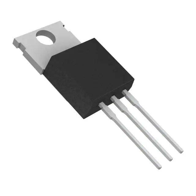
TO-220AB
Case 221A
Style 4
Additional Information
23
Datasheet
Resources
Samples
© 2020 Littelfuse, Inc.
Specifications are subject to change without notice.
Revised: 03/27/20
�Thyristors
8Amps Sen SCR
Maximum Ratings (TJ = 25°C unless otherwise noted)
Rating
Symbol
Value
Unit
VDRM,
VRRM
100
400
600
V
IT (RMS)
8.0
A
Peak Non-Repetitive Surge Current
(1/2 Cycle, Sine Wave 60 Hz, TJ = 110°C
ITSM
100
A
Circuit Fusing Consideration (t = 8.3 ms)
I2t
40
A²s
Forward Peak Gate Voltage (Pulse Width ≤ 10 µsec, TC= 83°C)
VGM
±5.0
V
Forward Peak Gate Current (Pulse Width ≤ 10 µsec, TC= 83°C)
IGM
1.0
A
Forward Peak Gate Power (Pulse Width ≤ 10 µsec, TC= 83°C)
PGM
5.0
W
Average Gate Power (t = 8.3 ms, TC = 83ºC)
Peak Repetitive Off−State Voltage (Note 1)
(− 40 to 110°C, Sine Wave, 50 to 60 Hz, Gate Open)
MCR72-3
MCR72-6
MCR72-8
On-State RMS Current
(180º Conduction Angles; TC = 83ºC)
PG(AV)
0.75
W
Operating Junction Temperature Range
TJ
-40 to +110
°C
Storage Temperature Range
Tstg
-40 to +150
°C
−
8.0
in. lb.
Mounting Torque
Stresses exceeding those listed in the Maximum Ratings table may damage the device. If any of these limits are exceeded, device functionality should not be assumed, damage may occur and reliability may be affected.
1. VDRM and VRRM for all types can be applied on a continuous basis. Ratings apply for zero or negative gate voltage; however, positive gate voltage shall not be applied concurrent with negative potential on the anode. Blocking voltages
shall not be tested with a constant current source such that the voltage ratings of the devices are exceeded.
Thermal Characteristics
Symbol
Value
Thermal Resistance, Junction-to-Case
Characterstic
RƟJC
2.2
Thermal Resistance, Junction-to-Ambient
RƟJA
60
TL
260
Maximum Lead Temperature for Soldering Purposes, 1/8” from
case for 10 seconds
Unit
°C/W
°C
Electrical Characteristics - OFF (TJ = 25°C unless otherwise noted)
Characteristic
Symbol
Min
Typ
IDRM
IRRM
-
-
10
-
-
500
ICCH
4
4
-
TJ = 25°C
Peak Repetitive Blocking Current
(VAK = VDRM = VRRM; RGK=1KΩ)
TJ = 110°C
High Logic Level Supply Current from VCC
Max
Unit
µA
Electrical Characteristics - ON (TJ = 25°C unless otherwise noted)
Characteristic
Symbol
Min
Typ
Max
Unit
VTM
_
1.7
2.0
V
Gate Trigger Current (Continuous dc) (Note 3) (VD = 12 V; RL = 100 Ω)
IGT
_
30
200
µA
Gate Trigger Voltage (Continuous dc) (Note 3) (VD = 12 V; RL = 100 Ω)
VGT
_
0.5
1.5
V
Gate Trigger Non-Trigger Voltage (VD = 12 Vdc, RL = 100 Ω, TJ = 110°C)
VGD
0.1
_
_
V
Holding Current
(VD = 12 V, Initiating Current = 200 mA, RGK = 1kΩ)
IH
_
_
6.0
mA
Gate Controlled Turn-On Time (Note 5)
(VD = Rated VDRM, ITM = 16 A, IG = 2 mA)
tgt
_
1.0
_
µs
Peak Forward On−State Voltage
(ITM = 16 A Peak, Pulse Width ≤ 1 ms, Duty Cycle ≤ 2%)
© 2020 Littelfuse, Inc.
Specifications are subject to change without notice.
Revised: 03/27/20
�Thyristors
8Amps Sen SCR
Dynamic Characteristics
Characteristic
Critical Rate−of−Rise of Off-State Voltage
(VD = Rated VDRM, Exponential Waveform, Gate Open, TJ = 110°C)
Symbol
Min
Typ
Max
Unit
dv/dt
-
10
−
V/µs
Product parametric performance is indicated in the Electrical Characteristics for the listed test conditions, unless otherwise noted. Product performance may not
be indicated by the Electrical Characteristics if operated under
different conditions.
2. Ratings apply for negative gate voltage or RGK = 1KΩ. Devices shall not have a positive gate voltage concurrently with a negative voltage on the anode. Devices should not be tested with a constant current source for forward and
reverse blocking capability such that the voltage applied exceeds the rated blocking voltage.
3. RGK current not included in measurement.
Voltage Current Characteristic of SCR
+Current
Symbol
Parameter
VDRM
Peak Repetitive Forward Off State Voltage
IDRM
Peak Forward Blocking Current
VRRM
Peak Repetitive Reverse Off State Voltage
IRRM
Peak Reverse Blocking Current
VTM
Maximum On State Voltage
IH
Holding Current
VTM
IRRM at VRRM
IH
Quadrant 3
Main Terminal 2-
Quadrant 1
Main Terminal 2+
IH
Off State
+Voltage
IDRM at VDRM
VTM
Figure 2. On−State Power Dissipation
PAV, Average Power Dissipation (Watts)
Figure 1. Average Current Derating
On State
16
dc
12
α
180º
α = Conduction Angl e
8.0
α = 30º
90º
60º
4.0
0
0
2.0
4.0
6.0
8.0
IT(AV), Average On-State Current (Amp)
Figure 3. Normalized Gate Current
Figure 4. Gate Voltage
© 2020 Littelfuse, Inc.
Specifications are subject to change without notice.
Revised: 03/27/20
�Thyristors
8Amps Sen SCR
Part Marking System
Dimensions
TO-220
Case 221A-01
Issue O
TO-220
Case 221A-09
Issue AH
4
TO-220AB
Case 221A
Style 3
SEATING
PLANE
B
F
12
S
1
4
Q
C
T
A
4
4
U
3
H
TO-220AB
Case 221A
Style 3
K
Z
TO-220AB
Case 221A
Style 3
YMAXX
MCR72-6TG
AKA
R
L
1
V
G
23
J
1
N
Inches
23
=Device Code
MCR72-x
Y
M
A
AKA
G
D
Dim
YMAXX
MCR72-xG
AKA
23
=Year
=Month
=Assembly Site
=Diode Polarity
=Pb-Free Package
Millimeters
Min
Max
Min
Max
A
0.590
0.620
14.99
15.75
B
0.380
0.420
9.65
10.67
C
0.178
0.188
4.52
4.78
D
0.025
0.035
0.64
0.89
3.73
MCR72-6T
Y
M
A
AKA
G
=Device Code
=Year
=Month
=Assembly Site
=Diode Polarity
=Pb-Free Package
Pin Assignment
1
Cathode
2
Anode
3
Gate
4
Anode
F
0.142
0.147
3.61
G
0.095
0.105
2.41
2.67
H
0.110
0.130
2.79
3.30
J
0.018
0.024
0.46
0.61
K
0.540
0.575
13.72
14.61
Device
L
0.060
0.075
1.52
1.91
N
0.195
0.205
4.95
5.21
MCR72−3G
Q
0.105
0.115
2.67
2.92
R
0.085
0.095
2.16
2.41
S
0.045
0.060
1.14
1.52
T
0.235
0.255
5.97
6.47
U
0.000
0.050
0.00
1.27
V
0.045
---
1.15
---
Z
---
0.080
---
2.04
Ordering Information
MCR72−6G
MCR72−6TG
MCR72−8G
Package
Shipping
TO−220AB
(Pb−Free)
500 Units / Box
MCR72−8TG
1. DIMENSIONING AND TOLERANCING PER ANSI Y14.5M, 1982.
2. CONTROLLING DIMENSION: INCH.
3. DIMENSION Z DEFINES A ZONE WHERE ALL BODY AND LEAD IRREGULARITIES ARE
ALLOWED.
Disclaimer Notice - Information furnished is believed to be accurate and reliable. However, users should independently evaluate the suitability of and test each product selected for their own applications. Littelfuse products are
not designed for, and may not be used in, all applications. Read complete Disclaimer Notice at http://www.littelfuse.com/disclaimer-electronics.
© 2020 Littelfuse, Inc.
Specifications are subject to change without notice.
Revised: 03/27/20
�
很抱歉,暂时无法提供与“MCR72-6G”相匹配的价格&库存,您可以联系我们找货
免费人工找货- 国内价格
- 1+13.10040
- 10+12.79800
- 30+12.60360
- 国内价格 香港价格
- 1+19.474861+2.51937
- 10+12.5189410+1.61952
- 100+8.55288100+1.10645
- 500+6.85432500+0.88671
- 1000+6.308301000+0.81608
- 2000+6.125782000+0.79247