Ignition IGBT
Surface Mount > 400v > NGB18N40ACLB
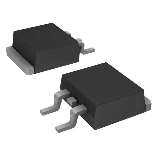
NGB18N40ACLB - 18 A, 400 V, N-Channel Ignition IGBT, D2PAK
Pb
Description
This Logic Level Insulated Gate Bipolar Transistor
(IGBT) features monolithic circuitry integrating ESD and
Over−Voltage clamped protection for use in inductive
coil drivers applications. Primary uses include Ignition,
Direct Fuel Injection, or wherever high voltage and high
current switching is required.
Features
• Ideal for Coil−on−Plug Applications
• DPAK Package Offers Smaller Footprint for Increased
Board Space
• Gate−Emitter ESD Protection
• Temperature Compensated Gate−Collector Voltage
18 Amps, 400 Volts
VCE (on) ≤ 2.0 V @
IC = 10 A, VGE ≥ 4.5 V
Clamp Limits Stress Applied to Load
• Integrated ESD Diode Protection
• New Design Increases Unclamped Inductive Switching
(UIS) Energy Per Area
Maximum Ratings (TJ = 25°C unless otherwise noted)
Rating
• Low Threshold Voltage Interfaces Power Loads to Logic
Symbol
Value
Unit
VCES
430
VDC
or Microprocessor Devices
• Low Saturation Voltage
Collector−Emitter Voltage
• High Pulsed Current Capability
• Optional Gate Resistor (RG) and Gate−Emitter
Collector−Gate Voltage
VCER
430
VDC
Resistor (RGE)
• Emitter Ballasting for Short−Circuit Capability
Gate−Emitter Voltage
Collector Current−Continuous
@ TC = 25°C − Pulsed
VGE
IC
18
VDC
18
ADC
50
AAC
ESD (Human Body Model) R = 1500
Ω, C = 100 pF
ESD
8.0
kV
ESD (Machine Model) R = 0 Ω, C =
200 pF
ESD
800
V
115
Watts
0.77
W/°C
Total Power Dissipation @ TC = 25°C
Derate above 25°C
Operating and Storage
Temperature Range
PD
TJ, Tstg
−55
to
+175
• These are Pb−Free Devices
Functional Diagram
Additional Information
°C
Stresses exceeding those listed in the Maximum Ratings table may damage the device.
If any of these limits are exceeded, device functionality should not be assumed, damage
may occur and reliability may be affected.
Datasheet
Resources
Samples
© 2018 Littelfuse, Inc.
Specifications are subject to change without notice.
Revised: 05/25/18
�Ignition IGBT
Surface Mount > 400v > NGB18N40ACLB
Unclamped Collector−To−Emitter Avalanche Characteristics (−55°≤ TJ ≤ 150°C)
Rating
Symbol
Value
Unit
Single Pulse Collector−to−Emitter Avalanche Energy
400
VCC = 50 V, VGE = 5.0 V, Pk IL = 21.1 A, L = 1.8 mH, Starting TJ = 25°C
mJ
EAS
300
VCC = 50 V, VGE = 5.0 V, Pk IL = 18.3 A, L = 1.8 mH, Starting TJ = 125°C
Reverse Avalanche Energy
VCC = 100 V, VGE = 20 V, Pk IL = 25.8 A, L = 6.0 mH, Starting TJ = 25°C
EAS (R)
2000
mJ
Maximum Short-Circuit Times (−55° ≤ TJ ≤ 150°C)
Rating
Symbol
Value
Unit
Short Circuit Withstand Time 1
(See Figure 17, 3 Pulses with 10 ms Period)
tsc1
750
µs
Short Circuit Withstand Time 2
(See Figure 18, 3 Pulses with 10 ms Period)
tsc2
5.0
ms
Symbol
Value
Unit
RθJC
1.3
°C/W
RθJA
50
°C/W
TL
275
°C
Thermal Characteristics
Rating
Thermal Resistance, Junction to Case
Thermal Resistance, Junction to Ambient
D2PAK (Note 1)
Maximum Lead Temperature for Soldering Purposes, 1/8” from case for
5 seconds
© 2018 Littelfuse, Inc.
Specifications are subject to change without notice.
Revised: 05/25/18
�Ignition IGBT
Surface Mount > 400v > NGB18N40ACLB
Electrical Characteristics - OFF
Characteristic
Collector−Emitter
Clamp Voltage
Zero Gate Voltage
Collector Current
Reverse Collector−Emitter
Leakage Current
Reverse Collector−Emitter
Clamp Voltage
Symbol
Test
Conditions
Temperature
Min
Typ
Max
IC = 2.0 mA
TJ = −40°C
to 150°C
380
395
420
IC = 10 mA
TJ = −40°C
to 150°C
390
405
430
TJ = 25°C
−
2.0
20
TJ = 150°C
−
10
40*
TJ = −40°C
−
1.0
10
TJ = 25°C
−
0.7
2.0
TJ = 150°C
−
12
25*
TJ = −40°C
−
0.1
1.0
TJ = 25°C
27
33
37
TJ = 150°C
30
36
40
TJ = −40°C
25
32
35
BVCES
ICES
IECS
BVCES(R)
VCE = 350
V, VGE = 0 V
VCE = −24 V
IC = −75 mA
Unit
VDC
µA
mA
VDC
Gate−Emitter Clamp Voltage
BVGES
IG = 5.0 mA
TJ = −40°C
to 150°C
11
13
15
VDC
Gate−Emitter Leakage Current
IGES
VGE = 10 V
TJ = −40°C
to 150°C
384
640
1000
µADC
Gate Emitter Resistor
RGE
−
TJ = −40°C
to 150°C
10
16
26
kΩ
© 2018 Littelfuse, Inc.
Specifications are subject to change without notice.
Revised: 05/25/18
�Ignition IGBT
Surface Mount > 400v > NGB18N40ACLB
Electrical Characteristics - ON (Note 2)
Characteristic
Symbol
Test
Conditions
IC = 6.0 A,
VGE = 4.0 V
IC = 8.0 A,
VGE = 4.0 V
IC = 10 A,
Collector−to−Emitter
On−Voltage
VCE(on)
VGE = 4.0 V
IC = 15 A,
VGE = 4.0 V
IC = 10 A,
VGE = 4.5 V
IC = 6.5 A,
VGE = 3.7 V
Forward Transconductance
gfs
VCE = 5.0 V,
IC = 6.0 A
Temperature
Min
Typ
Max
TJ = 25°C
1.0
1.4
1.6
TJ = 150°C
0.9
1.3
1.6
TJ = −40°C
1.1
1.45
1.7*
TJ = 25°C
1.3
1.6
1.9*
TJ = 150°C
1.2
1.55
1.8
TJ = −40°C
1.4
1.6
1.9*
TJ = 25°C
1.4
1.8
2.05
TJ = 150°C
1.5
1.8
2.0
TJ = −40°C
1.4
1.8
2.1*
TJ = 25°C
1.6
1.9
2.2
TJ = 150°C
1.7
2.1
2.3
TJ = −40°C
1.6
1.8
2.2
TJ = 25°C
1.3
1.8
2.0*
TJ = 150°C
1.3
1.75
2.0*
TJ = −40°C
1.4
1.8
2.0*
TJ = 25°C
_
_
1.65
TJ = −40°C
to 150°C
8.0
14
25
Unit
VDC
Mhos
Dynamic Characteristics
Characteristic
Symbol
Input Capacitance
CISS
Test
Conditions
VCC = 25 V,
Output Capacitance
COSS
VGE = 0 V
f = 1.0 MHz
Transfer Capacitance
CRSS
Temperature
TJ = −40°C
to
150°C
Min
Typ
Max
400
800
1000
50
75
100
4.0
7.0
10
Unit
pF
© 2018 Littelfuse, Inc.
Specifications are subject to change without notice.
Revised: 05/25/18
�Ignition IGBT
Surface Mount > 400v > NGB18N40ACLB
Switching Characteristics
Characteristic
Symbol
Test Conditions
Temperature
Min
Typ
Max
TJ = 25°C
−
4.0
10
Unit
VCC = 300 V,
Turn−Off Delay Time
(Resistive)
td(off)
IC = 6.5 A
RG = 1.0 kΩ,
RL = 46 Ω,
µS
VCC = 300 V,
Fall Time
(Resistive)
tf
IC = 6.5 A
RG = 1.0 kΩ,
TJ = 25°C
−
9.0
15
TJ = 25°C
−
0.7
4.0
RL = 46 Ω,
VCC = 10 V,
Turn−On Delay Time
td(on)
IC = 6.5 A
RG = 1.0 kΩ,
RL = 1.5 Ω,
µS
VCC = 10 V,
Rise Time
tr
IC = 6.5 A
RG = 1.0 kΩ,
TJ = 25°C
−
4.5
7.0
RL = 1.5 Ω,
*Maximum Value of Characteristic across Temperature Range.
1. When surface mounted to an FR4 board using the minimum recommended pad size.
2. Pulse Test: Pulse Width ≤ 300 µS, Duty Cycle ≤ 2%.
Ratings and Characteristic Curves
Figure 1. Output Characteristics
Figure 2. Output Characteristics
© 2018 Littelfuse, Inc.
Specifications are subject to change without notice.
Revised: 05/25/18
�Ignition IGBT
Surface Mount > 400v > NGB18N40ACLB
Figure 3. Output Characteristics
Figure 4. Transfer Characteristics
Figure 5. Collector−to−Emitter Saturation Voltage
versus Junction Temperature
Figure 6. Collector−to−Emitter Voltage versus
Gate−to−Emitter Voltage
Figure 7. Collector−to−Emitter Voltage versus
Gate−to−Emitter Voltage
Figure 8. Capacitance Variation
© 2018 Littelfuse, Inc.
Specifications are subject to change without notice.
Revised: 05/25/18
�Ignition IGBT
Surface Mount > 400v > NGB18N40ACLB
Figure 9. Gate Threshold Voltage versus Temperature
Figure 10. Minimum Open Secondary Latch Current
versus Temperature
Figure 11. Typical Open Secondary Latch Current
versus Temperature
Figure 12. Inductive Switching Fall Time
versus Temperature
Figure 13. Single Pulse Safe Operating Area
Figure 14. Single Pulse Safe Operating Area
(Mounted on an Infinite Heatsink at TA = 25°C)
(Mounted on an Infinite Heatsink at TA = 125°C)
© 2018 Littelfuse, Inc.
Specifications are subject to change without notice.
Revised: 05/25/18
�Ignition IGBT
Surface Mount > 400v > NGB18N40ACLB
Figure 15. Pulse Train Safe Operating Area
Figure 15. Pulse Train Safe Operating Area
(Mounted on an Infinite Heatsink at TC = 25°C)
(Mounted on an Infinite Heatsink at TC = 125°C)
Figure 17. Circuit Configuration for Short Circuit Test #1
Figure 18. Circuit Configuration for Short Circuit Test #2
© 2018 Littelfuse, Inc.
Specifications are subject to change without notice.
Revised: 05/25/18
�Ignition IGBT
Surface Mount > 400v > NGB18N40ACLB
Figure 19. Transient Thermal Resistance (Non−normalized Junction−to−Ambient mounted on minimum pad area)
t,TIME (S)
© 2018 Littelfuse, Inc.
Specifications are subject to change without notice.
Revised: 05/25/18
�Ignition IGBT
Surface Mount > 400v > NGB18N40ACLB
Soldering Footrpint
Dimensions
C
E
4
1
8.38
A
S
23
16.155
K
SEATING
PLANE
J
G
D 3 PL
0.13 (0.005 M) T B
VARIABLE
CONFIGURATION
ZONE
L
2X
1.016
1
L
Part Marking System
F
2
3
Inches
Millimeters
Min
Max
Min
Max
A
0.086
0.094
2.18
2.38
A1
0.000
0.005
0.00
0.13
b
0.025
0.035
0.63
0.89
b2
0.028
0.045
0.72
1.14
b3
0.180
0.215
4.57
5.46
c
0.018
0.024
0.46
0.61
c2
0.018
0.024
0.46
0.61
D
0.235
0.245
5.97
6.22
E
0.250
0.265
6.35
6.73
0.090 BSC
2.29 BSC
H
0.370
0.410
9.40
10.41
L
0.055
0.070
1.40
1.78
L1
0.114 REF
2.90 REF
L2
0.020 BSC
0.51 BSC
L3
DIMENSIONS: MILLIMETERS
M
F
5.080
PITCH
P
U
L
F
e
2X
3.504
M
M
Dim
W
H
N
R
M
10.49
V
W
0.035
0.050
0.89
L4
−−−
0.040
−−−
1.01
Z
0.155
−−−
3.93
−−−
ORDERING INFORMATION
Device
NGB18N40ACLBT4G
Package
Shipping†
DPAK
(Pb−Free)
2500 /
Tape & Reel
1.27
NOTES:
1. DIMENSIONING AND TOLERANCING PER ASME Y14.5M, 1994.
2. CONTROLLING DIMENSION: INCHES.
3. THERMAL PAD CONTOUR OPTIONAL WITHIN DIMENSIONS b3, L3 and Z.
4. DIMENSIONS D AND E DO NOT INCLUDE MOLD FLASH, PROTRUSIONS, OR BURRS. MOLD
FLASH, PROTRUSIONS, OR GATE BURRS SHALL NOT EXCEED 0.006 INCHES PER SIDE.
5. DIMENSIONS D AND E ARE DETERMINED AT THE OUTERMOST EXTREMES OF THE PLASTIC
BODY.
Disclaimer Notice - Information furnished is believed to be accurate and
reliable. However, users should independently evaluate the suitability
of and test each product selected for their own applications. Littelfuse
products are not designed for, and may not be used in, all applications.
Read complete Disclaimer Notice at: www.littelfuse.com/disclaimerelectronics.
6. DATUMS A AND B ARE DETERMINED AT DATUM PLANE H.
7. OPTIONAL MOLD FEATURE.
© 2018 Littelfuse, Inc.
Specifications are subject to change without notice.
Revised: 05/25/18
�