Ignition IGBT
Surface Mount > 410V > NGx15N41
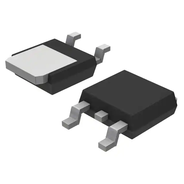
NGD15N41ACL, NGB15N41ACL, NGP15N41ACL - 15 A, 410 V, N-Channel Ignition IGBT, DPAK, D2PAK and TO-220
Description
This Logic Level Insulated Gate Bipolar Transistor (IGBT)
features monolithic circuitry integrating ESD and Over−
Voltage clamped protection for use in inductive coil
drivers applications. Primary uses include Ignition, Direct
Fuel Injection, or wherever high voltage and high current
switching is required.
Features
• Ideal for Coil−on−Plug Applications
• DPAK Package Offers Smaller Footprint and Increased
Board Space
• Gate−Emitter ESD Protection
15 Amps, 410 Volts
VCE(on) ≤ 2.1 V @
IC = 10 A, VGE ≥ 4.5 V
• Temperature Compensated Gate−Collector Voltage Clamp
Limits Stress Applied to Load
• Integrated ESD Diode Protection
• New Design Increases Unclamped Inductive Switching
(UIS) Energy Per Area
Maximum Ratings (TJ = 25°C unless otherwise noted)
Rating
Collector−Emitter Voltage
• Low Threshold Voltage to Interface Power Loads to Logic
Symbol
Value
Unit
VCES
440
VDC
or Microprocessor Devices
• Low Saturation Voltage
• High Pulsed Current Capability
• Optional Gate Resistor (RG) and Gate−Emitter
Collector−Gate Voltage
VCER
440
VDC
Resistor (RGE)
• These are Pb−Free Devices
Gate−Emitter Voltage
Collector Current−Continuous
@ TC = 25°C − Pulsed
VGE
IC
15
VDC
15
ADC
50
AAC
ESD (Human Body Model)
R = 1500 Ω, C = 100 pF
ESD
8.0
kV
ESD (Machine Model)
R = 0 Ω, C = 200 pF
ESD
800
V
107
W
0.71
W/°C
−55
to
+175
°C
Functional Diagram
C
G
RG
R GE
E
Total Power Dissipation @ TC = 25°C
Derate above 25°C
Operating and Storage
Temperature Range
PD
TJ, Tstg
Stresses exceeding Maximum Ratings may damage the device. Maximum Ratings are
stress ratings only. Functional operation above the Recommended Operating Conditions
is not implied. Extended exposure to stresses above the Recommended Operating Conditions may affect device reliability.
Additional Information
Datasheet
Resources
Samples
© 2018 Littelfuse, Inc.
Specifications are subject to change without notice.
Revised: 02/15/18
Pb
�Ignition IGBT
Surface Mount > 410V > NGx15N41
Unclamped Collector−To−Emitter Avalanche Characteristics (−55° ≤ TJ ≤ 175°C)
Rating
Symbol
Value
Unit
EAS
250
mJ
Single Pulse Collector−to−Emitter Avalanche Energy
VCC = 50 V, VGE = 5.0 V, Pk IL = 16.6 A, L = 1.8 mH, Starting TC = 25°C
VCC = 50 V, VGE = 5.0 V, Pk IL = 15 A, L = 1.8 mH, Starting TC = 125°C
200
Thermal Characteristics
Rating
Thermal Resistance, Junction to Case
Symbol
Value
RθJC
1.4
DPAK (Note 1)
Thermal Resistance, Junction to Ambient (Note 1)
D2PAK (Note 1)
100
°C/W
50
RθJA
TO−220
Maximum Lead Temperature for Soldering Purposes,
1/8” from case for 5 seconds
Unit
62.5
TL
°C
275
Electrical Characteristics - OFF
Characteristic
Collector−Emitter
Clamp Voltage
Zero Gate Voltage
Collector Current
Reverse Collector−Emitter
Leakage Current
Reverse Collector−Emitter
Leakage Current
Symbol
BVCES
ICES
ICES
BVCES(R)
Test
Conditions
Temperature
Min
Typ
Max
IC = 2.0 mA
TJ = −40°C
to 150°C
380
410
440
IC = 10 mA
TJ = −40°C
to 150°C
380
410
440
TJ = 25°C
−
2.0
20
TJ = 150°C
−
10
40*
TJ = −40°C
−
1.0
10
TJ = 25°C
−
0.7
2.0
TJ = 150°C
−
12
25*
TJ = −40°C
−
0.1
1.0
TJ = 25°C
27
33
37
TJ = 150°C
30
36
40
TJ = −40°C
25
31
35
VCE = 350 V
VGE = 0 V
VCE = −24 V
IC = -75 mA
Unit
VDC
µADC
mA
VDC
Gate−Emitter Clamp Voltage
BVGES
IG = 5.0 mA
TJ = −40°C
to 150°C
11
13
15
VDC
Gate−Emitter Leakage Current
IGES
VGE = ±10 V
TJ = −40°C
to 150°C
384
640
1000
µADC
Gate Resistor
RG
−
TJ = −40°C
to 150°C
−
70
−
Ω
Gate−Emitter Resistor
RGE
−
TJ = −40°C
to 150°C
10
16
26
kΩ
Gate Emitter Resistor
RGE
_
TJ = −40°C
to 150°C
14.25
16
25
kΩ
1. When surface mounted to an FR4 board using the minimum recommended pad size.
© 2018 Littelfuse, Inc.
Specifications are subject to change without notice.
Revised: 02/15/18
�Ignition IGBT
Surface Mount > 410V > NGx15N41
Electrical Characteristics - ON (Note 3)
Characteristic
Gate Threshold Voltage
Threshold Temperature
Coefficient (Negative)
Symbol
VGE (th)
−
Test Conditions
IC = 1.0 mA,
VGE = VCE
IC = 6.0 A
VGE = 4.0 V,
IC = 8.0 A
On−Voltage
VCE (on)
VGE = 4.0 V,
IC = 10 A
VGE = 4.5 V,
IC = 10 A
Forward Transconductance
gfs
Min
Typ
Max
TJ = 25°C
1.1
1.4
1.9
TJ = 150°C
0.75
1.0
1.4
TJ = −40°C
1.2
1.6
2.1*
−
−
3.4
−
TJ = 25°C
1.0
1.6
1.8
TJ = 150°C
0.9
1.5
1.8
TJ = −40°C
1.1
1.65
1.9*
TJ = 25°C
1.3
1.8
2.0*
TJ = 150°C
1.2
1.7
1.9
TJ = −40°C
1.4
1.8
2.0*
TJ = 25°C
1.4
2.0
2.2
TJ = 150°C
1.5
2.0
2.3*
TJ = −40°C
1.4
2.0
2.2
TJ = 25°C
1.3
1.9
2.1
TJ = 150°C
1.3
1.9
2.1
TJ = −40°C
1.4
1.95
2.1*
TJ = −40°C
to 150°C
8
15
25
−
VGE = 4.0 V,
Collector−to−Emitter
Temperature
VCE = 5.0 V,
IC = 6.0 A
Unit
VDC
mV/°C
VDC
Mhos
Dynamic Characteristics
Characteristic
Symbol
Input Capacitance
CISS
Test
Conditions
VCE = 25 V
Output Capacitance
Transfer Capacitance
COSS
CRSS
Temperature
Min
Typ
Max
400
650
1000
30
55
100
3.0
4.5
8.0
Unit
TJ = −40°C
VGE = 0 V
to
f = 1.0 MHz
150°C
© 2018 Littelfuse, Inc.
Specifications are subject to change without notice.
Revised: 02/15/18
pF
�Ignition IGBT
Surface Mount > 410V > NGx15N41
Switching Characteristics
Characteristic
Symbol
Test
Conditions
VCC = 300 V
Turn−On Delay Time
(Inductive)
td (off)
IC = 6.5 A
RG = 1.0 kΩ
L = 300 µH
VCC = 300 V
Fall Time
(Inductive)
tf
IC = 6.5 A
RG = 1.0 kΩ
L = 300 µH
Turn−Off Delay Time
(Resistive)
VCC = 300 V,
td (off)
IC = 6.5 A
RG = 1.0 kΩ,
RL = 46 Ω,
VCC = 300 V,
Fall Time
(Resistive)
tf
IC = 6.5 A
RG = 1.0 kΩ,
RL = 46 Ω,
Turn−Off Delay Time
(Inductive)
VCC = 10 V,
td(on)
IC = 6.5 A
RG = 1.0 kΩ,
RL = 1.5 Ω,
VCC = 10 V,
Rise Time
tr
IC = 6.5 A
RG = 1.0 kΩ,
RL = 1.5 Ω,
Temperature
Min
Typ
Max
TJ = 25°C
−
4.0
10
TJ = 150°C
−
4.5
10
TJ = 25°C
−
6.0
12
TJ = 150°C
−
10
12
TJ = 25°C
−
3.0
10
TJ = 150°C
−
3.5
10
TJ = 25°C
−
8.0
15
TJ = 150°C
−
12
15
TJ = 25°C
−
0.7
4.0
TJ = 150°C
−
0.7
4.0
TJ = 25°C
−
4.0
7.0
TJ = 150°C
−
5.0
7.0
µSec
*Maximum Value of Characteristic across Temperature Range.
3. Pulse Test: Pulse Width ≤ 300 µS, Duty Cycle ≤ 2%.
Ratings and Characteristic Curves
Figure 1. Output Characteristics
Unit
Figure 2. Output Characteristics
© 2018 Littelfuse, Inc.
Specifications are subject to change without notice.
Revised: 02/15/18
�Ignition IGBT
Surface Mount > 410V > NGx15N41
Figure 3. Output Characteristics
Figure 4. Transfer Characteristics
Figure 5. Collector−to−Emitter Saturation Voltage vs. Junction Temp
Figure 6. Collector−to−Emitter Voltage vs Gate−to−Emitter Voltage
Figure 7. Collector−to−Emitter Voltage vs Gate−to−Emitter Voltage
Figure 8. Capacitance Variation
10000
T J = 150 ϒC
IC = 15 A
2.5
IC = 10 A
2
IC = 5 A
1.5
1
0.5
0
38
4
59
C iss
1000
C, CAPACITANCE (pF)
COLLECTOR TO EMITTER VOLTAGE (VOLTS)
3
6
7
GATE TO EMITTER VOLTAGE (VOLTS)
10
100
C oss
10
C rss
1
0
0
200
40
61
80
100
120
40 160
180
V CE , COLLECTOR TO EMITTER VOLTAGE (VOLTS)
© 2018 Littelfuse, Inc.
Specifications are subject to change without notice.
Revised: 02/15/18
200
�Ignition IGBT
Surface Mount > 410V > NGx15N41
Figure 9. Gate Threshold Voltage vs.Temperature
Figure 10. Minimal Open Secondary Latch Current vs Temperature
30
2
1.8
Mean
Mean + 4 σ
IL , LATCH CURRENT (AMPS)
THRESHOLD VOLTAGE (VOLTS)
1.4
Mean
1.2
4 σ
1
0.8
0.6
0.4
0.2
0
50
30
10
10
50
30
70
V CC = 50 V
V GE = 5 V
R G = 1000 Ω
25
1.6
90
110
20
L = 6 mH
5
50
25
05
TEMPERATURE (°C)
75
100
125
150
175
12
V CC = 50 V
V GE = 5 V
R G = 1000 Ω
V CC = 300 V
V GE = 5 V
R G = 1000 Ω
IC = 10 A
L = 300 μH
10
SWITCHING TIME ( μs)
25
IL , LATCH CURRENT (AMPS)
50
Figure 12. Inductive Switching Fall Time vs. Temperature
30
L = 2 mH
15
L = 3 mH
10
L = 6 mH
8
tf
6
td(off)
4
2
5
0
2
TEMPERATURE ( °C)
Figure 11. Typical Open Secondary Latch Current vs Temperature
20
L = 3 mH
10
0
130 150
L = 2 mH
15
0
50
25
05
2
50
75
TEMPERATURE ( °C)
100
125
150
175
50
30
10
10
30
50
70
90
110
130 150
TEMPERATURE (°C)
© 2018 Littelfuse, Inc.
Specifications are subject to change without notice.
Revised: 02/15/18
�Ignition IGBT
Surface Mount > 410V > NGx15N41
Figure 13.Transient Thermal Resistance (Non−normalized Junction−to−Ambient mounted on fixture in Figure 14)
10
R(t), TRANSIENT THERMAL RESISTANCE (° C/Watt)
Duty Cycle = 0.5
0.2
1
0.1
0.05
0.02
0.1
0.01
D CURVES APPLY FOR POWER
PULSE TRAIN SHOWN
READ TIME AT T 1
P (pk)
t1
Single Pulse
t2
DUTY CYCLE, D = t
0.01
01. 0 0 0 0 1
0 .0 0 0 1
0 .0 0 1
0.01
0.
T J(pk) T A = P (pk) R θJA (t)
R θJC ≅ R(t) for t ≤ 0.2 s
1 /t2
11
0
100
1000
t,TIME (S)
Figure 14. Test Fixture for Transient Thermal Curve (48 square inches of 1/8 thick aluminum)
1.5 �
4�
4�
0.125 �
4�
© 2018 Littelfuse, Inc.
Specifications are subject to change without notice.
Revised: 02/15/18
�Ignition IGBT
Surface Mount > 410V > NGx15N41
Figure 16. Single Pulse Safe Operating Area
(Mounted on an Infinite Heatsink at TA = 125ºC)
Figure 15. Single Pulse Safe Operating Area
(Mounted on an Infinite Heatsink at TA = 25ºC)
100
100
100 µs
1 ms
1
10 ms
100 ms
0.1
0.01
1
10
100
1000
COLLECTOR CURRENT (AMPS)
COLLECTOR CURRENT (AMPS)
DC
10
10
DC
1
100 µs
0.1
1 ms
10 ms
0.01
100 ms
1
10
COLLECTOR EMITTER VOLTAGE (VOLTS)
100
100
t1 = 1 ms, D = 0.05
t1 = 1 ms, D = 0.05
t1 = 2 ms, D = 0.10
10
COLLECTOR CURRENT (AMPS)
COLLECTOR CURRENT (AMPS)
1000
Figure 18. Pulse Train Safe Operating Area
(Mounted on an Infinite Heatsink at TC = 125ºC)
Figure 17. Pulse Train Safe Operating Area
(Mounted on an Infinite Heatsink at TC = 25ºC)
t1 = 3 ms, D = 0.30
1
I(pk)
t1
0.1
t2
DUTY CYCLE, D = t
0.01
100
COLLECTOR EMITTER VOLTAGE (VOLTS)
1
10
COLLECTOR
1 /t2
100
EMITTER VOLTAGE (VOLTS)
1000
t1 = 2 ms, D = 0.10
10
t1 = 3 ms, D = 0.30
1
I(pk)
t1
0.1
0.01
t2
DUTY CYCLE, D = t
1
1 /t2
10
100
COLLECTOR EMITTER VOLTAGE (VOLTS)
© 2018 Littelfuse, Inc.
Specifications are subject to change without notice.
Revised: 02/15/18
1000
�Ignition IGBT
Surface Mount > 410V > NGx15N41
Soldering Footrpint
Dimensions
b3
A
Z
D
12
5.80
0.228
3.00
0.118
1.60
0.063
6.17
0.243
c
b
0.005 (0.13)
e
H
DETAIL A
3
b2
2.58
0.102
c2
B
4
L3
L4
6.20
0.244
C
A
E
M
C
H
L2
GAUGE
PLANE
C
L
mm
inches
SEATING
PLANE
A1
L1
DETAIL A
ROTATED 90 CW
Dim
Inches
Millimeters
Min
Max
Min
Max
A
0.086
0.094
2.18
2.38
A1
0.000
0.005
0.00
0.13
b
0.025
0.035
0.63
0.89
b2
0.030
0.045
0.76
1.14
b3
0.180
0.215
4.57
5.46
c
0.018
0.024
0.46
0.61
c2
0.018
0.024
0.46
0.61
D
0.235
0.245
5.97
6.22
E
0.250
0.265
6.35
6.73
e
0.090 BSC
0.370
0.410
9.40
10.41
L
0.055
0.070
1.40
1.78
L2
0.108 REF
0.020 BSC
A=
Y=
WW
G=
Assembly Location
Year
= Work Week
Pb Free Device
1
Gate
DPAK
CASE 369C
STYLE 7
2
Collector
YWW
GD
15N41G
4
Collector
3
Emitter
2.29 BSC
H
L1
Part Marking System
2.74 REF
0.51 BSC
L3
0.035
0.050
0.89
1.27
L4
−−−
0.040
−−−
1.01
Z
0.155
−−−
3.93
−−−
NOTES:
1. DIMENSIONING AND TOLERANCING PER ASME Y14.5M, 1994.
2. DIMENSION: INCHES.CONTROLLING
3. THERMAL PAD CONTOUR OPTIONAL WITHIN DI- MENSIONS b3, L3 and Z.
4. DIMENSIONS D AND E DO NOT INCLUDE MOLD FLASH, PROTRUSIONS, OR
BURRS. MOLD FLASH, PROTRUSIONS, OR GATE BURRS SHALL NOT EXCEED 0.006
INCHES PER SIDE.
5. DIMENSIONS D AND E ARE DETERMINED AT THE OUTERMOST EXTREMES OF
THE PLASTIC BODY.
6. DATUMS A AND B ARE DETERMINED AT DATUM PLANE H.
© 2018 Littelfuse, Inc.
Specifications are subject to change without notice.
Revised: 02/15/18
�Ignition IGBT
Surface Mount > 410V > NGx15N41
Dimensions
D2PAK
CASE 418B 04
ISSUE K
Dim
C
E
B
4
1
A
S
23
T
SEATING
PLANE
K
J
G
D 3 PL
0.13 (0.005)
VARIABLE
CONFIGURATION
ZONE
V
W
W
M
T B
R
L
M
M
F
VIEW W
1
WV
IEW W
2
A
0.340
0.380
8.64
9.65
B
0.380
0.405
9.65
10.29
0.190
4.06
4.83
0.020
0.035
0.51
0.89
E
0.045
0.055
1.14
1.40
F
0.310
0.350
7.87
8.89
IEW W
3
0.100 BSC
2.54 BSC
H
0.080
0.110
2.03
2.79
J
0.018
0.025
0.46
0.64
K
0.090
0.110
2.29
2.79
L
0.052
0.072
1.32
1.83
M
0.280
0.320
7.11
8.13
F
WV
Max
0.160
M
F
Min
C
P
U
L
Max
D
M
N
Millimeters
Min
G
H
Inches
W
N
0.197 REF
5.00 REF
P
0.079 REF
2.00 REF
R
0.039 REF
0.99 REF
S
0.575
0.625
14.60
15.88
V
0.045
0.055
1.14
1.40
NOTES:
1. DIMENSIONING AND TOLERANCING PER ANSI Y14.5M, 1982.
2. CONTROLLING DIMENSION: INCH.
3. 418B−01 THRU 418B−03 OBSOLETE, NEW STANDARD 418B−04.
Soldering Footrpint
Part Marking System
A=
Y=
WW
G=
10.49
Assembly Location
Year
= Work Week
Pb Free Device
8.38
4
Collector
16.155
NGB
15N41CLG
AYWW
2X
3.504
2X
1.016
5.080
PITCH
D2PAK
CASE 418B
STYLE 4
1
Gate
2
Collector
3
Emitter
DIMENSIONS: MILLIMETERS
© 2018 Littelfuse, Inc.
Specifications are subject to change without notice.
Revised: 02/15/18
�Ignition IGBT
Surface Mount > 410V > NGx15N41
Part Marking System
Dimensions
TO 220
CASE 221A 09
ISSUE AF
SEATING
PLANE
T
B
F
T
A=
Y=
WW
G=
Assembly Location
Year
= Work Week
Pb Free Device
C
S
4
Collector
4
A
Q
12
3
U
H
TO 220AB
CASE 221A
STYLE 9
K
Z
L
NGP
15N41CLG
AYWW
1
Gate
R
V
J
G
2
Collector
D
N
Dim
3
Emitter
Inches
Millimeters
Min
Max
Min
Max
A
0.570
0.620
14.48
15.75
B
0.380
0.405
9.66
10.28
C
0.160
0.190
4.07
4.82
D
0.025
0.035
0.64
0.88
F
0.142
0.161
3.61
4.09
G
0.095
0.105
2.42
2.66
H
0.110
0.155
2.80
3.93
J
0.014
0.025
0.36
0.64
K
0.500
0.562
12.70
14.27
L
0.045
0.060
1.15
1.52
N
0.190
0.210
4.83
5.33
Q
0.100
0.120
2.54
3.04
R
0.080
0.110
2.04
2.79
S
0.045
0.055
1.15
1.39
T
0.235
0.255
5.97
6.47
U
0.000
0.050
0.00
1.27
V
0.045
---
1.15
---
Z
---
0.080
---
2.04
NOTES:
1. DIMENSIONING AND TOLERANCING PER ANSI
Y14.5M, 1982.
2. CONTROLLING DIMENSION: INCH.
3. DIMENSION Z DEFINES A ZONE WHERE ALL
BODY AND LEAD IRREGULARITIES ARE
ALLOWED.
ORDERING INFORMATION
Device
Package
Shipping†
NGD15N41ACLT4G
DPAK
(Pb−Free)
2500 /
Tape & Reel
NGB15N41ACLT4G
D 2PAK
(Pb−Free)
800 /
Tape & Reel
NGP15N41ACLG
TO-220
(Pb−Free)
50 Units / Rail
†For information on tape and reel specifications, including part orientation and tape sizes,
please refer to our Tape and Reel Packaging Specification Brochure, BRD8011/D.
Disclaimer Notice - Information furnished is believed to be accurate and
reliable. However, users should independently evaluate the suitability of and
test each product selected for their own applications. Littelfuse products are
not designed for, and may not be used in, all applications. Read complete
Disclaimer Notice at: www.littelfuse.com/disclaimer-electronics.
© 2018 Littelfuse, Inc.
Specifications are subject to change without notice.
Revised: 02/15/18
�