NYC0102BLT1G
Sensitive Gate
Silicon Controlled Rectifiers
Reverse Blocking Thyristors
Littelfuse.com
Designed and tested for highly−sensitive triggering in low-power
switching applications.
Features
•
•
•
•
•
High dv/dt
Gating Current < 200 mA
Miniature SOT−23 Package for High Density PCB
SZ Prefix for Automotive and Other Applications Requiring Unique
Site and Control Change Requirements; AEC−Q101 Qualified and
PPAP Capable
These Devices are Pb−Free, Halogen Free/BFR Free and are RoHS
Compliant
0.25 AMP, 200 VOLT SCRs
G
A
K
MARKING
DIAGRAM
3
MAXIMUM RATINGS (TJ = 25°C unless otherwise noted)
Rating
Symbol
Peak Repetitive Off−State Voltage (Note 1)
(RGK = IK, TJ = *40 to +110°C, Sine
Wave, 50 to 60 Hz
VDRM,
VRRM
On-State Current RMS
(180° Conduction Angle, TC = 80°C)
IT(RMS)
0.25
A
Peak Non-repetitive Surge Current,
TA = 25°C, (1/2 Cycle, Sine Wave, 60 Hz)
ITSM
7.0
A
Circuit Fusing Considerations (t = 8.3 ms)
I2t
0.2
A2s
PGM
0.1
W
PG(AV)
0.02
W
Forward Peak Gate Current
(Pulse Width ≤ 20 ms, TA = 25°C)
IFGM
0.5
A
Reverse Peak Gate Voltage
(Pulse Width ≤ 1.0 ms, TA = 25°C)
VRGM
8.0
V
Operating Junction Temperature Range
@ Rated VRRM and VDRM
TJ
−40 to
+125
°C
Storage Temperature Range
Tstg
−40 to
+150
°C
Max
Unit
225
mW
380
°C/W
Forward Peak Gate Power
(Pulse Width ≤ 1.0 msec, TA = 25°C)
Forward Average Gate Power
(t = 8.3 msec, TA = 25°C)
Value
Unit
Total Device Dissipation FR− 5 Board
TA = 25°C
Thermal Resistance, Junction−to−Ambient
2
V
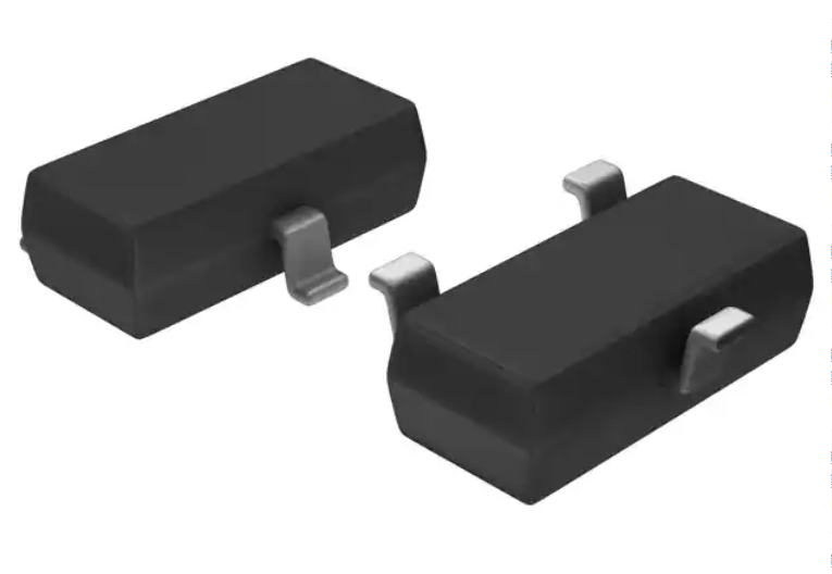
SOT−23
CASE 318
STYLE 8
200
Symbol
PD
RqJA
C2B MG
G
1
C2B = Specific Device Code
M
= Date Code*
G
= Pb−Free Package
(Note: Microdot may be in either location)
*Date Code orientation and/or overbar may vary depending upon manufacturing location.
PIN ASSIGNMENT
1
Cathode
2
Gate
3
Anode
ORDERING INFORMATION
Device
THERMAL CHARACTERISTICS
Characteristic
1
Package
Shipping
NYC0102BLT1G
SOT−23
(Pb−Free)
3000 / Tape &
Reel
SZNYC0102BLT1G
SOT−23
(Pb−Free)
3000 / Tape &
Reel
Stresses exceeding those listed in the Maximum Ratings table may damage the
device. If any of these limits are exceeded, device functionality should not be
assumed, damage may occur and reliability may be affected.
1. VDRM and VRRM for all types can be applied on a continuous basis. Ratings
apply for zero or negative gate voltage; however, positive gate voltage shall
not be applied concurrent with negative potential on the anode. Blocking
voltages shall not be tested with a constant current source such that the
voltage ratings of the devices are exceeded.
Specifications subject to change without notice. © 2016 Littelfuse, Inc.
September 19, 2016 − Rev. 2
1
Publication Order Number:
NYC0102BL/D
�NYC0102BLT1G
ELECTRICAL CHARACTERISTICS (TC = 25°C unless otherwise noted.)
Symbol
Characteristic
Min
Typ
Max
Unit
−
−
−
−
1.0
100
mA
mA
−
−
−
−
1.0
100
mA
mA
OFF CHARACTERISTICS
IDRM
Peak Repetitive Forward Blocking Current
(VDRM = 200 V, RGK = 1 kW)
TC = 25°C
TC = 125°C
Peak Repetitive Reverse Blocking Current
(VDRM = 200 V, RGK = 1 kW)
IRRM
TC = 25°C
TC = 125°C
ON CHARACTERISTICS
Peak Forward On−State Voltage
(ITM = 0.4 A, tp < 1 ms, TC = 25°C)
VTM
−
−
1.7
V
Gate Trigger Current
(VD = 12 V, RL = 100 W, TC = 25°C)
IGT
−
−
200
mA
Gate Trigger Voltage
(VD = 12 V, RL = 100 W, TC = 25°C)
VGT
−
−
0.8
V
Holding Current
(IT = 50 mA, RGK = 1 kW, TC = 25°C)
IH
−
−
6.0
mA
Gate Non−Trigger Voltage
(VD = VDRM , RL = 3.3 kW, TC = 125°C)
VGD
0.1
−
−
V
Latching Current
(IG = 1.0 mA, RGK = 1 kW, TC = 25°C)
IL
−
−
7.0
mA
VRG
8.0
−
−
V
Critical Rate of Rise of Off−State Voltage
(RGK = 1 kW, TC = 125°C)
dv/dt
200
−
−
V/ms
Critical Rate of Rise of On−State Current
(IG = 2xIGT 60 Hz, tr < 100 ns, TJ = 125°C)
di/dt
−
−
50
A/ms
Gate Reverse Voltage
(IRG = 10 mA)
DYNAMIC CHARACTERISTICS
Voltage Current Characteristic of SCR
+ Current
Symbol
Parameter
VDRM
Peak Repetitive Off State Forward Voltage
IDRM
Peak Forward Blocking Current
VRRM
Peak Repetitive Off State Reverse Voltage
IRRM
Peak Reverse Blocking Current
VTM
Peak on State Voltage
IH
Holding Current
Anode +
VTM
on state
IRRM at VRRM
Reverse Blocking Region
(off state)
Reverse Avalanche Region
IH
+ Voltage
IDRM at VDRM
Forward Blocking Region
(off state)
Anode −
Specifications subject to change without notice. © 2016 Littelfuse, Inc.
September 19, 2016 − Rev. 2
2
Publication Order Number:
NYC0102BL/D
�NYC0102BLT1G
0.3
IT, AVERAGE CURRENT (A)
P, AVERAGE POWER (W)
0.25
0.2
0.15
0.1
0.05
0
DC
0.2
0.15
180°
0.1
0.05
0
0
0.05
0.1
0.15
0
0.2
50
150
IT, AVERAGE CURRENT (A)
T, TEMPERATURE (°C)
Figure 2. Current Derating
1
TRANSIENT RESISTANCE
(NORMALIZED)
6
5
4
3
2
1
0
1
10
100
0.8
0.6
0.4
0.2
0
1.E−04 1.E−03 1.E−02 1.E−01 1.E+00 1.E+01 1.E+02 1.E+03
1000
NUMBER OF CYCLES
PULSE DURATION (s)
Figure 3. Surge Current ITSM vs. Number of
Cycles
Figure 4. Thermal Response
10
2
Gate
Open
1.5
ITM, (A)
100
Figure 1. Maximum Average Power vs.
Average Current
7
ITSM (A)
0.25
RGK = 1k
1
1
125°C
25°C
0.1
0
0.5
1
0.5
1.5
2
0
2.5
200
VTM, (V)
September 19, 2016 − Rev. 2
300
350
400
TJ, (K)
Figure 5. ON−State Characteristics
Specifications subject to change without notice. © 2016 Littelfuse, Inc.
250
Figure 6. Gate Trigger Current vs. TJ
(Normalized to 255C)
3
Publication Order Number:
NYC0102BL/D
�NYC0102BLT1G
0.07
2
0.06
Gate
Open
0.05
IGT (mA)
1.5
RGK = 1k
1
0.04
0.03
0.02
0.5
0.01
0 200
250
300
350
0
400
0
2
4
6
8
10
TJ, (K)
RGK, (kW)
Figure 7. Gate Trigger Current vs. TJ
(Normalized to 255C)
Figure 8. Gate Trigger Current vs. RGK
25
12
2000
20
dV/dt (V/ms)
1500
IH,IL (mA)
15
10
500
5.0
0
1000
0
1
2
3
4
6
5
RGK, (kW)
7
8
9
0
0
10
2
Figure 9. Holding and Latching Current vs.
RGK
4
6
RGK, (kW)
8
10
12
Figure 10. dV/dt vs. RGK
1.0
VGT (V)
0.80
0.60
0.40
0.20
0
200
250
300
350
400
TJ, (K)
Figure 11. Gate Triggering Voltage vs. TJ
Specifications subject to change without notice. © 2016 Littelfuse, Inc.
September 19, 2016 − Rev. 2
4
Publication Order Number:
NYC0102BL/D
�NYC0102BLT1G
PACKAGE DIMENSIONS
SOT−23 (TO−236)]
CASE 318−08
ISSUE AP
NOTES:
1. DIMENSIONING AND TOLERANCING PER ANSI Y14.5M, 1982.
2. CONTROLLING DIMENSION: INCH.
3. MAXIMUM LEAD THICKNESS INCLUDES LEAD FINISH
THICKNESS. MINIMUM LEAD THICKNESS IS THE MINIMUM
THICKNESS OF BASE MATERIAL.
4. DIMENSIONS D AND E DO NOT INCLUDE MOLD FLASH,
PROTRUSIONS, OR GATE BURRS.
D
SEE VIEW C
3
HE
E
DIM
A
A1
b
c
D
E
e
L
L1
HE
q
c
1
2
b
0.25
e
q
A
L
A1
MIN
0.89
0.01
0.37
0.09
2.80
1.20
1.78
0.10
0.35
2.10
0°
MILLIMETERS
NOM
MAX
1.00
1.11
0.06
0.10
0.44
0.50
0.13
0.18
2.90
3.04
1.30
1.40
1.90
2.04
0.20
0.30
0.54
0.69
2.40
2.64
−−−
10 °
MIN
0.035
0.001
0.015
0.003
0.110
0.047
0.070
0.004
0.014
0.083
0°
INCHES
NOM
0.040
0.002
0.018
0.005
0.114
0.051
0.075
0.008
0.021
0.094
−−−
MAX
0.044
0.004
0.020
0.007
0.120
0.055
0.081
0.012
0.029
0.104
10°
STYLE 8:
PIN 1. ANODE
2. NO CONNECTION
3. CATHODE
L1
VIEW C
SOLDERING FOOTPRINT
0.95
0.037
0.95
0.037
2.0
0.079
0.9
0.035
SCALE 10:1
0.8
0.031
mm Ǔ
ǒinches
Littelfuse products are not designed for, and shall not be used for, any purpose (including, without limitation, automotive, military,
aerospace, medical, life-saving, life-sustaining or nuclear facility applications, devices intended for surgical implant into the body, or
any other application in which the failure or lack of desired operation of the product may result in personal injury, death, or property
damage) other than those expressly set forth in applicable Littelfuse product documentation. Warranties granted by Littelfuse shall be
deemed void for products used for any purpose not expressly set forth in applicable Littelfuse documentation. Littelfuse shall not be
liable for any claims or damages arising out of products used in applications not expressly intended by Littelfuse as set forth in
applicable Littelfuse documentation. The sale and use of Littelfuse products is subject to Littelfuse Terms and Conditions of Sale,
unless otherwise agreed by Littelfuse.
Littelfuse.com
Specifications subject to change without notice. © 2016 Littelfuse, Inc.
September 19, 2016 − Rev. 2
5
Publication Order Number:
NYC0102BL/D
�