SIDACtor® Protection Thyristors
Broadband OptimizedTM Protection
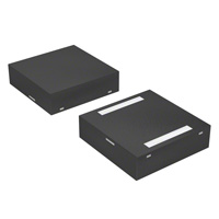
Q2L Series - 3x3 QFN
RoHS
Pb e3
Description
Q2L Series 3x3 QFN are low capacitance SIDACtor®
thyristors designed to protect high density broadband
equipment from damaging overvoltage transients.
The series provides a low profile surface solution that
enables broadband equipment to comply with global
regulatory standards while limiting the impact to
broadband signals and board space.
Agency Approvals
Features and Benefits
Agency
• �Low voltage overshoot
Agency File Number
• �RoHS Compliant and
Halogen-Free
• �Low on-state voltage
E133083
• Pb-free E3 means 2nd level
interconnect is Pb-free and
the terminal finish material
is tin(Sn) (IPC/JEDEC
J-STD-609A.01)
• �Low capacitance
• �Does not degrade surge
capability after multiple
surge events within limit.
Schematic Symbol
• Small footprint
• �Recognized to UL 497B
as an Isolated Loop Circuit
• �Fails short circuit when
Protector
surged in excess of ratings
Applicable Global Standards
Additional Information
Datasheet
Resources
Samples
• �TIA-968-A
• �GR 1089 Inter-building*
• �TIA-968-B
• GR 1089 Intra-building
• �ITU K.20/21/45 Enhanced
Level*
• �YD/T 1082
• YD/T 993
• ��ITU K.20/21/45 Basic Level
• YD/T 950
• �IEC 61000-4-5 2nd edition
* A/B-Rated parts require series resistance
© 2020 Littelfuse, Inc.
Specifications are subject to change without notice.
Revised: 05/08/20
�SIDACtor® Protection Thyristors
Broadband OptimizedTM Protection
Electrical Characteristics
Part Number
Marking
P0080Q12ALRP
P0300Q12ALRP
P0640Q12ALRP
P0720Q12ALRP
P0900Q12ALRP
P1100Q12ALRP
P1200Q12ALRP
P1300Q12ALRP
P1500Q12ALRP
P1800Q12ALRP
P2000Q12ALRP
P2300Q12ALRP
P2500Q12ALRP
P2600Q12ALRP
P3100Q12ALRP
P3500Q12ALRP
P0080Q12BLRP
P0300Q12BLRP
P0640Q12BLRP
P0720Q12BLRP
P0900Q12BLRP
P1100Q12BLRP
P1200Q12BLRP
P1300Q12BLRP
P1500Q12BLRP
P1800Q12BLRP
P2000Q12BLRP
P2300Q12BLRP
P2500Q12BLRP
P2600Q12BLRP
P3100Q12BLRP
P3500Q12BLRP
P-8A
P03A
P06A
P07A
P09A
P11A
P12A
P13A
P15A
P18A
P20A
P23A
P25A
P26A
P31A
P35A
P-8B
P03B
P06B
P07B
P09B
P11B
P12B
P13B
P15B
P18B
P20B
P23B
P25B
P26B
P31B
P35B
V
DRM
@lDRM=5µA
V min
6
25
58
65
75
90
100
120
140
170
180
190
230
220
275
320
6
25
58
65
75
90
100
120
140
170
180
190
230
220
275
320
VS
@100V/µs
V max
25
40
77
88
98
130
130
160
180
220
220
260
290
300
350
450
25
40
77
88
98
130
130
160
180
220
220
260
290
300
350
400
IH
mA min
IS
mA max
IT
A max
50
50
150
150
150
150
150
150
150
150
150
150
150
150
150
150
50
50
150
150
150
150
150
150
150
150
150
150
150
150
150
150
800
800
800
800
800
800
800
800
800
800
800
800
800
800
800
800
800
800
800
800
800
800
800
800
800
800
800
800
800
800
800
800
2.2
2.2
2.2
2.2
2.2
2.2
2.2
2.2
2.2
2.2
2.2
2.2
2.2
2.2
2.2
2.2
2.2
2.2
2.2
2.2
2.2
2.2
2.2
2.2
2.2
2.2
2.2
2.2
2.2
2.2
2.2
2.2
Capacitance
@1MHz, 2V bias
pF Min
pF Max
25
55
15
35
40
60
40
60
35
55
30
50
30
50
25
45
25
40
25
35
25
35
25
35
25
35
25
35
20
35
20
30
25
55
15
35
40
60
40
60
35
55
30
50
30
50
25
45
25
40
25
35
25
35
25
35
25
35
25
35
20
35
20
30
VT@ IT =
2.2Amps
V max
5
5
5
5
5
5
5
5
5
5
5
5
5
5
5
5
5
5
5
5
5
5
5
5
5
5
5
5
5
5
5
5
Notes:
- Absolute maximum ratings measured at TA= 25ºC (unless otherwise noted).
- Components are bi-directional.
Surge Ratings
ITSM
Ipp
Series
2/10µs
1.2/50µs/8/20µs
10/160µs
10/560µs
10/1000µs
50 / 60 Hz
di/dt
A min
A min
A min
A min
A min
A min
A/µs max
A
150
150
90
50
45
20
500
B
250
250
150
100
80
25
500
Notes:
- Peak pulse current rating (IPP) is repetitive and guaranteed for the life of the product.
- IPP ratings applicable over temperature range of -40ºC to +85ºC
- The component must initially be in thermal equilibrium with -40°C < TJ < +150°C
Thermal Considerations
Package
Symbol
Value
Unit
3x3 QFN
TJ
Operating Junction Temperature Range
-40 to +150
°C
TS
Storage Temperature Range
-65 to +150
°C
120
°C/W
RƟJA
Parameter
Thermal Resistance: Junction to Ambient
© 2020 Littelfuse, Inc.
Specifications are subject to change without notice.
Revised: 05/08/20
�SIDACtor® Protection Thyristors
Broadband OptimizedTM Protection
tr x td Pulse Waveform
V-I Characteristics
IPP – Peak Pulse Current – %IPP
+I
IT
IS
IH
IDRM
-V
+V
VT
VDRM
VS
tr = rise time to peak value
td = decay time to half value
Peak
Value
100
Waveform = tr x td
50
Half Value
0
td
tr
0
t – Time (µs)
-I
Normalized VS Change vs. Junction Temperature
Normalized DC Holding Current vs. Case Temperature
Percent of VS Change – %
10
IH
8
6
25 °C
2
0
-4
1.8
1.6
1.4
0.8
0.6
-6
0.4
-8
-40 -20
0
25°C
1.2
1.0
Ratio of
4
IH (TC = 25ºC)
2.0
14
12
-40
20 40 60 80 100 120 140 160
-20
0
20
40
60
80
100 120 140
160
Case Temperature (TC) - ºC
Junction Temperature (TJ) – °C
Soldering Parameters
Reflow Condition
Pre Heat
Pb-Free assembly
- Temperature Min (Ts(min))
+150°C
- Temperature Max (Ts(max))
+200°C
- Time (Min to Max) (ts)
60-180 secs.
Figure 1
TP
- Temperature (TL) (Liquidus)
+217°C
- Temperature (tL)
60-150 secs.
Peak Temp (TP)
+260(+0/-5)°C
Time within 5°C of actual Peak Temp (tp)
30 secs. Max.
Ramp-down Rate
6°C/sec. Max.
Time 25°C to Peak Temp (TP)
8 min. Max.
Do not exceed
+260°C
Temperature
Reflow
3°C/sec. Max.
Critical Zone
TL to TP
Ramp-up
Average ramp up rate (Liquidus Temp (TL) to peak) 3°C/sec. Max.
TS(max) to TL - Ramp-up Rate
tP
TL
T S(max)
tL
Ramp-down
T S(min)
Preheat
tS
25
time to peak temperature
(t 25ºC to peak)
Time
© 2020 Littelfuse, Inc.
Specifications are subject to change without notice.
Revised: 05/08/20
�SIDACtor® Protection Thyristors
Broadband OptimizedTM Protection
Physical Specifications
Environmental Specifications
Lead Material
Copper Alloy
Terminal Finish
100% Matte-Tin Plated
UL Recognized epoxy meeting flammability
classification V-0
Body Material
High Temp Voltage
Blocking
80% Rated VDRM (VAC Peak ) +125°C or +150°C,
504 or 1008 hrs. MIL-STD-750 (Method 1040)
JEDEC, JESD22-A-101
Temp Cycling
-65°C to +150°C, 15 min. dwell, 10 up to 100
cycles. MIL-STD-750 (Method 1051) EIA/
JEDEC, JESD22-A104
52 VDC (+85°C) 85%RH, 504 up to 1008 hrs.
EIA/JEDEC, JESD22-A-101
+150°C 1008 hrs. MIL-STD-750 (Method 1031)
High Temp Storage
JEDEC, JESD22-A-101
Low Temp Storage
-65°C, 1008 hrs.
0°C to +100°C, 5 min. dwell, 10 sec. transfer,
Thermal Shock
10 cycles. MIL-STD-750 (Method 1056)
JEDEC, JESD22-A-106
Resistance to Solder Heat +260°C, 30 secs. MIL-STD-750 (Method 2031)
85%RH, +85°C, 168 hrs., 3 reflow cycles
Moisture Sensitivity Level
(+260°C Peak). JEDEC-J-STD-020, Level 1
Biased Temp & Humidity
Can be A or B
Dimensions — 3x3 QFN
TOP VIEW
C
A
A
E
J
B
F
2.15
1.93
END VIEW
N2
N1
H
K1
SIDE VIEW
M1
M2
Inches
Dimensions
BOTTOM VIEW
0.585
K2
Recommended
Soldering Pad Outline
(Reference Only)
Part Numbering
Max
Min
Max
0.114
0.122
2.900
3.100
3.100
B
0.114
0.122
2.900
C
0.075
0.083
1.900
2.100
E
0.011
0.019
0.285
0.485
2.130
F
0.076
0.084
1.930
H
0.035
0.043
0.900
1.100
J
0.000
0.008
0.000
0.200
K1
0.004
0.012
0.100
0.300
K2
0.004
0.012
0.100
0.300
M1
0.056
0.064
1.430
1.630
M2
0.038
0.046
0.970
1.170
N1
0.096
0.104
2.440
2.640
N2
0.082
0.090
2.080
2.280
Part Marking
Terminals on Back
P xxx 0 Q12 x L RP
TYPE
P = SIDACtor
MEDIAN VOLTAGE
CONSTRUCTION
VARIABLE
Millimeters
Min
REEL PACK
RoHS COMPLIANT
IPP RATING
XXXX
XXXXX
Part Marking Code
(Refer to Electrical Characteristics Table)
Date code
PACKAGE TYPE
Packing Options
Package
Type
Q12
Description
Quantity
3x3 QFN Tape and Reel Pack
5000
Added
Suffix
RP
Industry
Standard
EIA-481-D
© 2020 Littelfuse, Inc.
Specifications are subject to change without notice.
Revised: 05/08/20
�SIDACtor® Protection Thyristors
Broadband OptimizedTM Protection
Tape and Reel Dimensions — 3x3 QFN
Reel Dimension
Symbols
C
A
D
N
W1
B
Tape Leader and Trailer Dimensions
END
START
CARRIER TAPE
COVER TAPE
TRAILER
160mm MIN
LEADER
400mm MIN
Tape Dimension Items
D0
P0
P2
T
CARRIER TAPE
D1
B0 F
W0
K0
P1
A0
E1
E2W
Description
Inches
Millimeters
Min
Max
Min
Max
N/A
12.992
N/A
330.0
A
Reel Diameter
B
Drive Spoke Width
0.059
N/A
1.50
C
Arbor Hole Diameter
0.504
0.531
12.80
13.50
D
Drive Spoke Diameter
0.795
N/A
20.20
N/A
N
Hub Diameter
1.969
N/A
50.00
N/A
W1
Reel Inner Width at Hub
0.488
0.567
12.40
14.40
A0
Pocket Width at bottom
0.126
0.134
3.20
3.40
B0
Pocket Length at bottom
0.126
0.134
3.20
3.40
D0
Feed Hole Diameter
0.059
0.063
1.50
1.60
D1
Pocket Hole Diameter
0.059
N/A
1.50
N/A
E1
Feed hole position 1
0.065
0.073
1.65
1.85
E2
Feed hole position 2
0.400
0.408
10.15
10.35
F
Feed hole
center-Pocket hole
0.215
0.219
5.45
5.55
K0
Pocket Depth
0.039
0.051
1.00
1.30
P0
Feed Hole Pitch
0.153
0.161
3.90
4.10
P1
Component Spacing
0.311
0.319
7.90
8.10
P2
Feed hole
center-Pocket hole
0.077
0.081
1.95
2.05
T
Carrier Tape Thickness
0.010
0.014
0.25
0.35
W
Embossed Carrier
Tape Width
0.453
0.484
11.50
12.30
W0
Cover Tape Width
0.358
0.366
9.10
9.30
N/A
COVER TAPE
Disclaimer Notice - Information furnished is believed to be accurate and reliable. However, users should independently evaluate the suitability of and test each product selected for their own applications. Littelfuse products are
not designed for, and may not be used in, all applications. Read complete Disclaimer Notice at: www.littelfuse.com/disclaimer-electronics.
© 2020 Littelfuse, Inc.
Specifications are subject to change without notice.
Revised: 05/08/20
�