Thyristors Datasheet
SxX8BBS Series
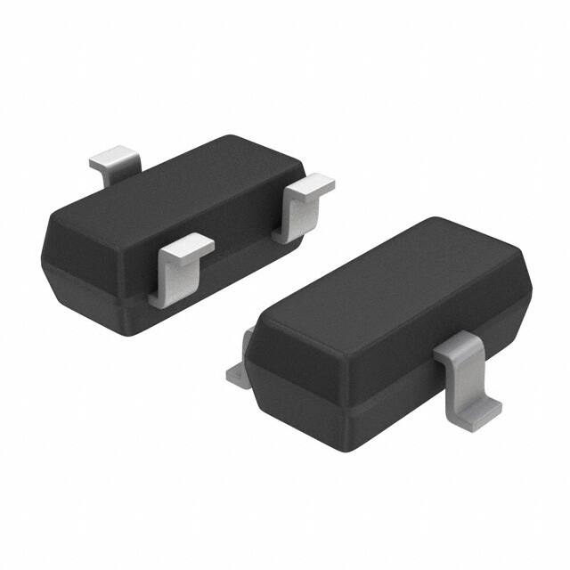
EV Series 0.8 Amp Sensitive SCRs
RoHS
Description
This new sensitive SCR component series offers 600V V DRM and
0.8A IT(RMS) capability in the smallest package size in the industry,
SOT23. It is specifically designed for GFCI (Ground Fault Circuit
Interrupter) applications. All SCRs junctions are glass-passivated to
ensure long term reliability and parametric stability.
Features
■ High dv/dt noise immunity
■ Very compact SOT23 SMT
package
■ Improved turn-off time (tq) <
25 μsec
■ Surge current capability up to
12A @ 60Hz
Main Features
Symbol
Value
Unit
IT(RMS)
0.8
A
VDRM / VRRM
600
V
IGT
200
μA
■ �RoHS compliant and HalogenFree
Applications
The SxX8BBS series is specifically designed for GFCI (Ground
Fault Circuit Interrupter) and applications.
Schematic Symbol
Pin out
G
K
■ Sensitive gate for direct
microprocessor interface
■ Blocking voltage
( VDRM / VRRM )
capability - up to 600V
Anode
3
A
1
2
Cathode
Gate
Absolute Maximum Ratings
Symbol
Parameter
Pw=100μs
Value
Unit
700
V
A
VDSM/ VRSM
Peak non-repetitive blocking voltage
IT(RMS)
RMS on-state current (full sine wave)
TC = 80°C
0.8
IT(AV)
Average on-state current
TC = 80°C
0.51
A
ITSM
Non repetitive surge peak on-state current
(Single cycle, TJ initial = 25°C)
f= 50Hz
10
A
f= 60Hz
12
A
I2t
I2t Value for fusing
tp = 10 ms
f= 50 Hz
0.5
A2s
tp = 8.3 ms
f= 60 Hz
0.6
A 2s
di/dt
Critical rate of rise of on-state current IG = 10mA
60 Hz
TJ = 125°C
80
A/µs
IGM
Peak Gate Current
tp = 20 μs
TJ = 125°C
1.0
A
PG(AV)
Average gate power dissipation
—
TJ = 125°C
0.1
W
Tstg
Storage junction temperature range
—
—
-40 to 150
°C
TJ
Operating junction temperature range
—
—
-40 to 125
°C
1
© 2021 Littelfuse, Inc.
Specifications are subject to change without notice.
Revised: GD. 08/03/21
�Thyristors Datasheet
SxX8BBS Series
EV Series 0.8 Amp Sensitive SCRs
Electrical Characteristics (TJ = 25°C, unless otherwise specified)
Symbol
Description
Test Conditions
Limit
Value
Unit
IGT
DC Gate Trigger Current
VD = 6V, RL = 100 Ω
VGT
DC Gate Trigger Voltage
VD = 6V, RL = 100 Ω
VGRM
Peak Reverse Gate Voltage
IRG = 10μA
MIN.
8
V
IH
Holding Current
Initial Current = 20mA
MAX.
10
mA
(dv/dt)s
Critical Rate-of-Rise of
Off-State Voltage
TJ = 125°C
VD = 67%VDRM /VRRM
Exp. Waveform, RGK =1 kΩ
MIN.
50
V/μs
VGD
Gate Non-Trigger Voltage
VD = VDRM, RGK =1 kΩ
TJ = 125°C
MIN.
0.2
V
tq
Turn-Off Time
IT=0.5A
MAX.
25
μs
tgt
Turn-On Time
IG=10mA,Pw= 15μsec,
IT = 1.6A(pk)
TYP.
2.0
μs
MIN.
50
μA
MAX.
200
μA
MAX.
0.8
V
Static Characteristics (TJ = 25°C, unless otherwise specified)
Symbol
Description
Test Conditions
Limit
Value
Unit
VTM
Peak On-State Voltage
ITM = 1.6A (pk)
MAX.
1.70
V
IDRM/IRRM
VDRM/VRRM
TJ = 25°C
MAX.
5
μA
TJ = 125°C
MAX.
100
μA
Thermal Resistances
Symbol
Description
Value
Unit
RƟ(JC)
Junction to case (AC)
45
°C/ W
RƟ(J-A)
Junction to ambient
220
°C/ W
Figure 1:
Normalized DC Gate Trigger Current vs.
Junction Temperature
Figure 2:
Normalized DC Holding Current vs.
Junction Temperature
1.8
3.00
1.6
IH
2.00
1.50
IH (TJ = 25°C)
1.4
Ratio of
IGT
Ratio of
IGT (TJ = 25°C)
2.50
1.00
0.50
1.2
1
0.8
0.6
0.4
0.2
0.00
-40
-15
10
35
60
85
110
0
135
-40
Junction Temperature (TJ) - °C
-15
10
35
60
85
110
135
Junction Temperature (TJ) - °C
2
© 2021 Littelfuse, Inc.
Specifications are subject to change without notice.
Revised: GD. 08/03/21
�Thyristors Datasheet
SxX8BBS Series
EV Series 0.8 Amp Sensitive SCRs
Figure 3:
Normalized DC Gate Trigger Voltage vs. Junction Temperature
Figure 4:
On-State Current vs. On-State Voltage (Typical)
1
0.8
0.6
0.4
0.2
0
-40
-15
10
35
60
85
110
4
Intantaneous On -state Current (IT) – Amps
VGT (TJ = 25°C)
1.2
Ratio of
VGT
1.4
135
3.5
3
2.5
2
1.5
1
0.5
0
0.8
0.9
1
1.1
1.2
130
0.8
Maximum Allowable Case Temperature
(TC) - oC
CURRENT WAVEFORM: Sinusoidal
LOAD: Resistive or Inductive
CONDUCTION ANGLE: 180o
0.7
1.3
1.4
1.5
1.6
1.7
1.8
1.9
2
Figure 6:
Maximum Allowable Case Temperature vs. On-State Current
Figure 5:
Power Dissipation (Typical) vs. RMS On-State Current
Average On-state Power Dissipation
[PD(AV)] - Watts
0.7
Instantaneous On -state Voltage (VT ) – Volts
Junction Temperature (TJ) - °C
CURRENT WAVEFORM: Sinusoidal
LOAD: Resistive or Inductive
CONDUCTION ANGLE: 180o
CASE TEMPERATURE: Measured as
shown on dimensional drawings
120
0.6
110
100
0.5
0.4
0.3
0.2
0.1
90
80
70
60
50
0.0
0.0
0.1
0.2
0.3
0.4
0.5
0.6
0.7
0.8
0.0
0.1
0.2
0.3
0.4
0.5
0.6
0.7
0.8
RMS On-state Current [IT(RMS)] - Amps
RMS On-state Current [IT(RMS)] - Amps
Figure 7: Surge Peak On-State Current vs. Number of Cycles
Peak Surge (Non-repetitive) On-State
Current (IT S M) – Amps
20
10
Supply Frequency: 60Hz Sinusoidal
Load: Resistive
RMS On-State Current [IT(RMS)]: Max Rated Value at
Specific Case Temperature
0.8
AD
Notes:
1. Gate control may be lost during and immediately
following surge current interval.
2. Overload may not be repeated until junction
temperature has returned to steady-state rated value.
evi
ces
1
1
10
100
1000
Surge Current Duration - Full Cycle
3
© 2021 Littelfuse, Inc.
Specifications are subject to change without notice.
Revised: GD. 08/03/21
�Thyristors Datasheet
SxX8BBS Series
EV Series 0.8 Amp Sensitive SCRs
Figure 9:
Static dv/dt vs. CGK vs. Juntion Temperature
Figure 8:
Static dv/dt vs. RGK vs. Junction Temperature
5000
5000
25ºC
1000
Typical dv/dt value (V/µs)
Typical dv/dt Value (V/µs)
VD=400V
25ºC
125ºC
100
85ºC
10
85ºC
1000
125ºC
100
10
VD=400V
RGK=1kΩ
1
100
1
1000
10000
1
50
10
RGK Resistance (Ω)
CGK Value (nF)
Soldering Parameters
Pre Heat
Pb – Free assembly
- Temperature Min (Ts(min))
150°C
- Temperature Max (Ts(max))
200°C
- Time (min to max) (ts)
60 – 120 secs
Average ramp up rate (Liquidus Temp) (TL) to peak 3°C/second max
TS(max) to TL - Ramp-up Rate
Reflow
5°C/second max
- Temperature (TL) (Liquidus)
217°C
- Time (min to max) (ts)
60 – 150 seconds
Peak Temperature (TP)
260
Time within 5°C of actual peak Temperature (tp)
30 seconds
Ramp-down Rate
6°C/second max
Time 25°C to peak Temperature (TP)
8 minutes Max.
Do not exceed
260°C
+0/-5
tP
TP
Temperature
Reflow Condition
tL
TS(max)
Preheat
TS(min)
°C
25
4
Ramp-up
TL
Ramp-do
Ramp-down
tS
time to peak temperature
Time
© 2021 Littelfuse, Inc.
Specifications are subject to change without notice.
Revised: GD. 08/03/21
�Thyristors Datasheet
SxX8BBS Series
EV Series 0.8 Amp Sensitive SCRs
Physical Specifications
Reliability/Environmental Tests
Terminal Finish
100% Matte Tin-plated.
Body Material
UL Recognized compound meeting
flammability rating V-0.
Lead Material
Copper Alloy
Test
Specifications and Conditions
HTRB (AC Blocking)
MIL-STD-750, M-1040, Cond A Applied Peak
AC voltage @ VDRM @ 125°C for 1008 hours
Temperature Cycling
MIL-STD-750, M-1051,
100 cycles; -55°C to +150°C; 15-min dwell-time
H3TRB
EIA / JEDEC, JESD22-A101
1008 hours; 160V - DC: 85°C; 85%
rel humidity
UHAST
ESD22-A118, 96hours, 130°C, 85%RH
Resistance to
Solder Heat
MIL-STD-750 Method 2031, 260°C, 10s
Solderability
ANSI/J-STD-002, category 3, Test A
Moisture Sensitivity
Level
Level 1, JEDEC-J-STD-020D
Design Considerations
Careful selection of the correct component for the application’s
operating parameters and environment will go a long way toward
extending the operating life of the Thyristor. Good design practice
should limit the maximum continuous current through the main
terminals to 75% of the component rating. Other ways to ensure
long life for a power discrete semiconductor are proper heat
sinking and selection of voltage ratings for worst case conditions.
Overheating, overvoltage (including dv/dt), and surge currents are
the main killers of semiconductors. Correct mounting, soldering,
and forming of the leads also help protect against component
damage.
Dimensions – SOT-23
D
Anode
Dimensions
SEE VIEW C
Max
Min
Typ
Max
A
0.04
0.04
0.04
0.89
1.02
1.12
A1
0.00
0.00
0.01
0.01
0.10
0.15
b
0.02
0.02
0.02
0.38
0.46
0.51
c
0.00
0.01
0.01
0.08
0.13
0.18
D
0.11
0.11
0.12
2.80
2.90
3.04
E
0.05
0.05
0.06
1.19
1.30
1.40
L1
e
0.07
0.08
0.08
1.78
1.91
2.06
VIEW C
L
0.02
0.02
0.02
0.40
0.49
0.60
L1
0.01
0.02
0.03
0.36
0.53
0.74
H
0.08
0.09
0.10
2.10
2.30
2.64
Ɵ
0°
-
10°
0°
-
10°
c
b
e
Cathode
0.25
Gate
A
L
A1
Millimeters
Typ
HE
E
Inches
Min
SOLDERING FOOTPRINT
0.8
0.031
mm
inches
SCALE 10:1
0.9
0.035
2.0
0.079
0.95
0.037
0.95
0.037
Product Selector
Part Number
S6X8BBS
Voltage
600V
X
Packing Options
Gate Sensitivity
Package
Part Number
Marking
Weight
Packing
Mode
Base
Quantity
200 μA
SOT-23
S6X8BBSRP
6X8
0.01g
Tape & Reel
3000
5
© 2021 Littelfuse, Inc.
Specifications are subject to change without notice.
Revised: GD. 08/03/21
�Thyristors Datasheet
SxX8BBS Series
EV Series 0.8 Amp Sensitive SCRs
SOT-23 Reel Pack (RP) Specifications
4mm
4 mm
Ø1.5 mm
2 mm
1.75 mm
3.5 mm
8 mm
180 mm
13 mm Abor
Hole Diameter
11.6 mm
DIRECTION OF FEED
Part Numbering System
Part Marking System
S xX8 B B S xx
Series
S: SCR
Voltage
6: 600V
Current
X8: 0.8A
Packing Type
RP: Reel Pack
6X8
YML
Sensitivity & Type
S: 200µA Sensitive SCR
Package Type
BB: SOT-23
Date Code Marking
Y:Year Code
M: Month Code
L: Location Code
Disclaimer Notice - Information furnished is believed to be accurate and reliable. However, users should independently evaluate the suitability of and test each product selected for their own applications. Littelfuse products are
not designed for, and may not be used in, all applications. Read complete Disclaimer Notice at http://www.littelfuse.com/disclaimer-electronics.
6
© 2021 Littelfuse, Inc.
Specifications are subject to change without notice.
Revised: GD. 08/03/21
�
很抱歉,暂时无法提供与“S6X8BBSRP”相匹配的价格&库存,您可以联系我们找货
免费人工找货- 国内价格 香港价格
- 1+8.208461+1.01943
- 10+5.0926610+0.63247
- 100+3.31007100+0.41109
- 500+2.54307500+0.31583
- 1000+2.295731000+0.28511
- 国内价格 香港价格
- 3000+1.783373000+0.22148
- 6000+1.640946000+0.20379
- 9000+1.589969000+0.19746
- 国内价格 香港价格
- 3000+1.680313000+0.20868
- 6000+1.653506000+0.20535
- 9000+1.644569000+0.20424
- 12000+1.6356212000+0.20313
- 15000+1.6088115000+0.19980
- 国内价格
- 1+2.04120
- 10+1.98720
- 30+1.95480
- 100+1.92240


 工商网监
湘ICP备2023018690号
工商网监
湘ICP备2023018690号
