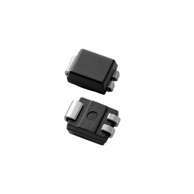
Sx02CSx
Thyristor Datasheet
Teccor® brand Thyristors
Sx02CSx Series 1.25 Amp Sensitive SCRs
Product Description
The Sx02CSx offers excellent unidirectional
switches for phase control applications such as
heating and motor speed controls.
Sensitive gate SCRs are easily triggered with
microAmps of current as furnished by sense coils,
proximity switches, and microprocessors.
Features
• RoHS compliant
• Glass-passivated junctions
• Voltage capability up to 800 V
• Surge capability up to 20 A
Agency Approvals and Environmental
Environmental Approvals
Applications
Typical applications are capacitive discharge
systems for strobe lights and gas engine ignition.
They also include controls for power tools,
home/brown goods, and white goods appliances
Product Summary
Characteristic
Value
Unit
A
IT(RMS)
1.25
VDRM / VRRM
800
V
IGT
50 to 200
µA
Schematic Symbol
1
Specifications are subject to change without notice.
Read complete Disclaimer Notice at www.littelfuse.com/disclaimer-electronics.
© 2021 Littelfuse, Inc.
Revised: 6/2/2021
�Sx02CSx
Thyristor Datasheet
1. Maximum Ratings ...........................................................................................................................................3
2. Thermal Characteristics ..................................................................................................................................3
3. Electrical Characteristics (TJ = 25 °C unless otherwise specified) .................................................................3
4. Static Characteristics ......................................................................................................................................3
5. Performance Curves .......................................................................................................................................4
6. Soldering Parameters .....................................................................................................................................7
7. Physical Specifications ....................................................................................................................................7
8. Environmental Specifications..........................................................................................................................7
9. Design Considerations ....................................................................................................................................7
10. Package Dimensions ....................................................................................................................................8
11. Part Numbering and Marking ........................................................................................................................8
12. Packing Options ............................................................................................................................................8
13. Packing Specifications ..................................................................................................................................9
2
Specifications are subject to change without notice.
Read complete Disclaimer Notice at www.littelfuse.com/disclaimer-electronics.
© 2021 Littelfuse, Inc.
Revised: 6/2/2021
�Sx02CSx
Thyristor Datasheet
1. Maximum Ratings
Symbol
Characteristic
Conditions
Value
Unit
V
VDSM
Non-repetitive Peak Off-state Voltage
TJ = 25°C, tp = 1 ms, RGK = 220
1250
VRSM
Non-repetitive Peak Reverse Voltage
TJ = 25°C, tp = 1 ms, RGK = 220
900
V
IT(RMS)
RMS On-state Current
TC = 75 °C
1.25
A
IT(AV)
Average On-state Current
TC = 75 °C
0.8
A
ITSM
Peak Non-repetitive Surge Current (Single Half
Cycle, TJ,Initial = 25 °C)
f = 50 Hz
16
f = 60 Hz
20
I2t
I2t Value for Fusing
tp = 8.3 ms
1.6
A2s
50
A/µs
di/dt
Critical Rate of Rise of On-state Current
IGM
f = 60 Hz
TJ = 110 °C
A
Peak Gate Current
TJ = 110 °C
1.0
A
PG(AV)
Average Gate Power Dissipation
TJ = 110 °C
0.1
W
TSTG
Storage Temperature
-
-40 to 150
°C
Operating Junction Temperature
-
-40 to 110
°C
TJ
2. Thermal Characteristics
Symbol
Rth(JC)
Characteristic
Value
Unit
1
Thermal Resistance, junction-to-case (AC)
60
°C/W
2
Footnote 1: Mounted on 1 cm copper (two-ounce) foil surface
3. Electrical Characteristics (T
J
Symbol
= 25 °C unless otherwise specified)
Description
Conditions
Min
S802CS1
Typ
Max
Min
S802CS2
Typ
Max
Unit
IGT
DC Gate Trigger Current
VD = 6 V, RL = 10
-
-
50
-
-
200
µA
VGT
DC Gate Trigger Voltage
VD = 6 V, RL = 10
-
-
0.8
-
-
0.8
V
VGRM
Peak Reverse Gate Voltage
5
-
-
5
-
-
V
-
-
3
-
-
5
mA
10
-
-
15
-
-
V/µs
-
-
50
-
-
50
µs
-
3
-
-
20
-
µs
0.25
-
-
0.25
-
-
V
IH
IRG = 10 µA
Holding Current
dv/dt
IT = 20 mA (initial), RGK
Critical Rate-of-rise of Off-stage
Voltage
VD =VDRM, RGK
TJ = 110°C
tq
Turn-off Time
tgt
Turn-on Time
IG = 2 x IGT, PW = 15
Gate Non-trigger Voltage
VD = VDRM, RL
VGD
IT = 1 A, tp = 50
, dv/dt = 5
, di/dt = 5
, IT = 1.6 A
J
= 110°C
4. Static Characteristics
Symbol
VTM
IDRM/IRRM
Description
Peak On-state Voltage
Conditions
IT = 2.5 A; tp
Off-state Current, Peak Repetitive
(VDRM = VRRM, RGK = 1
)
3
Value (Max)
1.70
TJ = 25°C
1
TJ = 100°C
50
TJ = 110°C
500
Unit
V
µA
Specifications are subject to change without notice.
Read complete Disclaimer Notice at www.littelfuse.com/disclaimer-electronics.
© 2021 Littelfuse, Inc.
Revised: 6/2/2021
�Sx02CSx
Thyristor Datasheet
5. Performance Curves
Figure 2. Normalized DC Gate Trigger Voltage vs. Junction
Temperature
4.0
2.0
3.0
1.5
Ratio of
VGT / VGT (TJ = 25 °C)
Ratio of
IGT / IGT (TJ = 25 °C)
Figure 1. Normalized DC Gate Trigger Current vs. Junction
Temperature
2.0
1.0
0.0
1.0
0.5
0.0
-40
-15
10
35
60
85
110
-40
-15
Junction Temperature, TJ (°C)
Figure 3. Normalized DC Holding Current vs. Junction
Temperature
Instantaneous On-state Current, IT (A)
Ratio of IH / IH
(TJ = 25 °C)
2.5
2
1.5
1
0.5
0
-15
10
35
60
35
60
85
110
Figure 4. Typical On-state Current vs. On-state Voltage
3
-40
10
Junction Temperature, TJ (°C)
85
110
10
TJ = 25°C
8
6
4
2
0
0.7
Junction Temperature, TJ (°C)
0.8
0.9
1
1.1
1.2
1.3
1.4
1.5
1.6
Instantaneous On-state Voltage, VT (V)
4
Specifications are subject to change without notice.
Read complete Disclaimer Notice at www.littelfuse.com/disclaimer-electronics.
© 2021 Littelfuse, Inc.
Revised: 6/2/2021
�Sx02CSx
Thyristor Datasheet
Figure 5. Typical Power Dissipation vs. RMS On-state Current
Figure 6. Maximum Allowable Case Temperature vs. RMS Onstate Current
Max Allowable Case Temperature, TC (°C)
Average On-state Power Dissipation,
PD (W)
0.7
0.6
0.5
0.4
0.3
0.2
0.1
115
105
95
85
Current Waveform: Sinusoidal
Load: Resistive or Inductive
Conduction Angle: 180°
75
65
0
0
0
0.1
0.2
0.3
0.4
0.5
0.6
0.7
0.8
0.2
0.4
0.6
0.8
1
1.2
1.4
RMS On-state Current, IT(RMS) (A)
RMS On-state Current, IT(RMS) (A)
Figure 7. Maximum Allowable Case Temperature vs. Average Onstate Current
Figure 8. Peak Capacitor Discharge Current
Peak Discharge Current, ITM (A)
Max Allowable Case Temperature, TC (°C)
180
115
105
95
85
Current Waveform: Sinusoidal
Load: Resistive or Inductive
Conduction Angle: 180°
75
160
140
1 Hz
120
12 Hz
100
60 Hz
80
60
40
20
0
1
65
0
0.2
0.4
0.6
0.8
1
10
100
Pulse Current Duration, tw (µs)
Average On-state Current, IT(AVE) (A)
Figure 9. Peak Repetitive Sinusoidal Pulse Current
Peak Discharge Current, ITM (A)
180
160
140
1 Hz
120
100
12 Hz
80
60 Hz
60
40
20
0
1
10
100
Pulse Current Duration, tw (µs)
5
Specifications are subject to change without notice.
Read complete Disclaimer Notice at www.littelfuse.com/disclaimer-electronics.
© 2021 Littelfuse, Inc.
Revised: 6/2/2021
�Sx02CSx
Thyristor Datasheet
Peak Surge (Non-repetitive) On-state
Current, ITSM (A)
Figure 10. Surge Peak On-state Current vs. Number of Cycles
100.0
Notes
1. Gate control may be lost during and immediately
following surge current interval.
2. Overload may not be repeated until junction
temperature has returned to steady-state rated value.
10.0
1.0
Supply Frequency: 60 Hz Sinusoidal
Load: Resistive
RMS Onstate Current [IT,RMS]: Max rated value at specific case temperature
0.1
1
10
100
1000
Surge Current Duration - Full Cycle
Figure 11. Simple Test Circuit for Gate Trigger Voltage and Current
Notes
V1
VGT
IG
R1
0 V to 10 V dc meter
0 V to 1 V dc meter
0 mA to 1 mA dc milliammeter
1 k potentiometer
To measure gate trigger voltage and current, raise gate
voltage (VGT) until meter reading V1 drops from 6 V to 1
V. Gate trigger voltage is the reading on VGT just prior to
V1 dropping. Gate trigger current IGT Can be computed
from the relationship.
IGT = IG- - VGT /1000 A
where IG is reading (in amperes) on meter just prior to
V1 dropping.
2. IGT may turn out to be a negative quantity (trigger
current flows out from gate lead). If negative current
occurs, IGT value is not a valid reading. Remove 1 k
resistor and use IG as the more correct IGT value. This will
occur on 12 µA gate products.
6
Specifications are subject to change without notice.
Read complete Disclaimer Notice at www.littelfuse.com/disclaimer-electronics.
© 2021 Littelfuse, Inc.
Revised: 6/2/2021
�Sx02CSx
Thyristor Datasheet
6. Soldering Parameters
Parameter
Value
Reflow Condition
Pre-Heat
Pb-free Assembly
Temperature Min, TS(Min)
150 °C
Temperature Max, TS(Max)
200 °C
Time (Min to Max), ts
60 to 180 s
Average Ramp-up Rate Liquidus Temp., TL to peak
5 °C/s (Max)
TS(Max) to TL Ramp-up Rate
5 °C/s (Max)
Temperature, TL Liquidus
Reflow
217 °C
Time, tS
60 to 150 s
Peak Temperature, TP
260 °C (±5 °C)
Time within 5 °C of Actual Peak Temperature, tP
20 to 40 s
Ramp-down Rate
5 °C/s (Max)
Time 25 °C to Peak Temperature, TP
8 minutes (Max)
Do Not Exceed
7. Physical Specifications
Device Feature
280 °C
8. Environmental Specifications
Detail
Terminal Finish
100% Matte Tin-plated/ Pb-free Solder Dipped
Body Material
UL Recognized epoxy meeting Flammability Rating V-0
Lead Material
Copper Alloy
Test
AC Blocking
Temperature Cycling
Temperature/Humidity
High Temperature
Storage
Low Temperature
Storage
Resistance to Solder
Heat
9. Design Considerations
Careful selection of the correct component for the
will go a long way toward extending the operating life
of the Thyristor. Good design practice should limit the
maximum continuous current through the main
terminals to 75% of the component rating. Other
ways to ensure long life for a power discrete
semiconductor are proper heat sinking and selection
of voltage ratings for worst case conditions.
Overheating, overvoltage (including dv/dt), and surge
currents are the main killers of semiconductors.
Correct mounting, soldering, and forming of the leads
also help protect against component damage.
7
Specifications and Conditions
MIL-STD-750, M-1040, Cond A Applied Peak
AC voltage @ 110°C for 1008 hours
MIL-STD-750, M-1051, 100 cycles, -40°C to
+150°C, 15 min dwell time
EIA / JEDEC, JESD22-A101 1008 hours;
320V - DC: 85°C; 85% relative humidity
MIL-STD-750, M-1031, 1008 hours, 150°C
1008 hours, -40°C
MIL-STD-750 Method 2031
Solderability
ANSI/J-STD-002, category 3, Test A
Lead Bend
MIL-STD-750, M-2036 Cond E
Specifications are subject to change without notice.
Read complete Disclaimer Notice at www.littelfuse.com/disclaimer-electronics.
© 2021 Littelfuse, Inc.
Revised: 6/2/2021
�Sx02CSx
Thyristor Datasheet
10. Package Dimensions
Compak (C Package)
Inches
Dimension
Millimeters
Min
Max
Min
Max
A
0.130
0.156
3.30
3.95
B
0.201
0.220
5.10
5.60
C
0.077
0.087
1.95
2.20
D
0.159
0.181
4.05
4.60
E
0.030
0.063
0.75
1.60
F
0.075
0.096
1.90
2.45
G
0.002
0.008
0.05
0.20
H
0.077
0.104
1.95
2.65
J
0.043
0.053
1.09
1.35
K
0.006
0.016
0.15
0.41
L
0.030
0.055
0.76
1.40
M
0.022
0.028
0.56
0.71
N
0.027
0.033
0.69
0.84
P
0.052
0.058
1.32
1.47
11. Part Numbering and Marking
12. Packing Options
Part Number
Marking
Gate Sensitivity
Weight
Packing Mode
Base Quantity
S802CS1RP
S802S1
50 µA
0.08 g
Embossed Carrier
2500
S802CS2RP
S802S2
200 µA
0.08 g
Embossed Carrier
2500
8
Specifications are subject to change without notice.
Read complete Disclaimer Notice at www.littelfuse.com/disclaimer-electronics.
© 2021 Littelfuse, Inc.
Revised: 6/2/2021
�Sx02CSx
Thyristor Datasheet
13. Packing Specifications
Compak Embossed Carrier Reel Pack (RP) Specifications
Meets all EIA-481-1 Standards
For additional information please visit www.Littelfuse.com/powersemi
Disclaimer Notice - Littelfuse products are not designed for, and shall not be used for, any purpose (including, without limitation, automotive, military, aerospace, medical, lifesaving, life-sustaining or nuclear facility applications, devices intended for surgical implant into the body, or any other application in which the failure or lack of desired operation of
the product may result in personal injury, death, or property damage) other than those expressly forth in applicable Littelfuse product documentation. Littelfuse shall not be liable for
any claims or damages arising out of products used in applications not expressly intended by Littelfuse as set forth in applicable Littelfuse documentation.
Read complete Disclaimer Notice at www.littelfuse.com/disclaimer-electronics
9
Specifications are subject to change without notice.
Read complete Disclaimer Notice at www.littelfuse.com/disclaimer-electronics.
© 2021 Littelfuse, Inc.
Revised: 6/2/2021
�