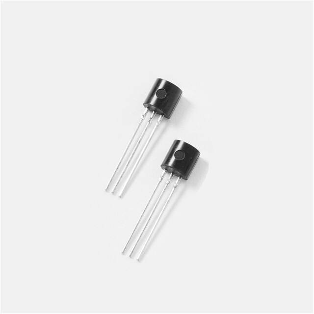
S802xSx
Thyristor Datasheet
S802xSx Series
EV Series 1.5 Amp Sensitive SCRs
Product Description
The S802xSx offers a high static dv/dt with a low
turn off (tq) time. It is specifically designed for GFCI
(Ground Fault Circuit Interrupter) and AFCI (Arc
Fault Circuit Interrupter), RCD (Residual Current
Device) and RCBO (Residual Current Circuit
Breaker with Overload Protection) applications.
All SCR junctions are glass-passivated to ensure
long term reliability and parametric stability.
Features
Agency Approvals and Environmental
• Surge current capability up to 24 A
• Blocking voltage (VDRM / VRRM) capability up to
800 V
• Non-repetitive direct surge peak off-state voltage
(VDSM) up to 1250 V
• Non-repetitive reverse surge peak off-state
voltage (VRSM) up to 900 V
• High dv/dt noise immunity
• Improved turn-off time (tq)
• Sensitive gate for direct microprocessor interface
• Halogen-free and RoHS compliant
Environmental Approvals
Product Summary
Characteristic
Value
Unit
IT(RMS)
1.5
A
VDRM / VRRM
800
V
VDSM (tp = 50 µs)
1250
V
VRSM (tp = 50 µs)
900
V
IGT
20 to 100
µA
Applications
• GFCI
• AFCI
• RCD
• RCBO
Schematic Symbol
*TO-92 with GAK pin output
1
Specifications are subject to change without notice.
Read complete Disclaimer Notice at www.littelfuse.com/disclaimer-electronics.
© 2021 Littelfuse, Inc.
Revised: 6/10/2021
�S802xSx
Thyristor Datasheet
1. Maximum Ratings...........................................................................................................................................3
2. Thermal Characteristics ..................................................................................................................................3
3. Electrical Characteristics (TJ = 25 °C, unless otherwise specified) ................................................................3
4. Static Characteristics (TJ = 25 °C, unless otherwise specified) ......................................................................3
5. Performance Curves .......................................................................................................................................4
6. Soldering Parameters .....................................................................................................................................6
7. Physical Specifications....................................................................................................................................6
8. Environmental Specifications..........................................................................................................................6
9. Design Considerations ....................................................................................................................................6
10. Package Dimensions ....................................................................................................................................7
11. Part Numbering and Marking ........................................................................................................................8
12. Product Selector ...........................................................................................................................................8
13. Packing Options ............................................................................................................................................8
14. Packing Specifications ..................................................................................................................................8
2
Specifications are subject to change without notice.
Read complete Disclaimer Notice at www.littelfuse.com/disclaimer-electronics.
© 2021 Littelfuse, Inc.
Revised: 6/10/2021
�S802xSx
Thyristor Datasheet
1. Maximum Ratings
Symbol
Characteristic
Conditions
IT(RMS)
RMS On-state Current (Full Sine Wave)
IT(AV)
Average On-state Current
ITSM
Non-repetitive Surge Peak On-state Current (Sine
Half Wave, TJ,Initial = 25 °C)
I2t
I2t Value for Fusing
di/dt
IGM
TO-92
TC = 65 °C
SOT-223
TC = 80 °C
TO-92
TC = 65 °C
SOT-223
TC = 80 °C
Unit
1.5
A
0.9
A
f = 50 Hz
20.0
f = 60 Hz
24.0
f = 50 Hz
2.0
A2s
TJ = 125 °C
80
A/µs
tp = 20 µs
TJ = 125 °C
0.5
A
tp = 10 ms
Critical Rate of Rise of On-state Current IG =10 mA
Peak Gate Current
Value
A
PG(AV)
Average Gate Power Dissipation
-
TJ = 125 °C
0.2
W
TSTG
Storage Junction Temperature Range
-
-
-40 to 150
°C
Operating Junction Temperature Range
-
-
-40 to 125
°C
Value
Unit
TJ
2. Thermal Characteristics
Symbol
Characteristic
Rth(JC)
Thermal Resistance, junction-to-case (AC)
IT = 1.5 ARMS1
Rth(JA)
Thermal Resistance, junction-to-ambient (AC)
IT = 1.5 ARMS1
TO-92
35
SOT-223
25
TO-92
150
SOT-223
60
°C/W
°C/W
Footnote 1: 60 Hz AC resistive load condition, 100% conduction
3. Electrical Characteristics (T
J
Symbol
= 25 °C, unless otherwise specified)
Description
Conditions
Value
Typ
Min
Max
Unit
IGT
DC Gate Trigger Current
VD = 6 V, RL = 10
20
60
100
µA
VGT
DC Gate Trigger Voltage
VD = 6 V, RL = 10
-
-
0.8
V
8
-
-
V
-
-
3
mA
VGRM
IH
dv/dt
VGD
Peak Reverse Gate Voltage
IRG = 10 µA
Holding Current
RGK
Critical Rate-of-rise of Off-stage Voltage
Gate Non-trigger Voltage
tq
Turn-off Time
tgt
Turn-on Time
RGK
TJ = 125 °C, VD = 67% of
VDRM, Exponential waveform
VD = ½ VDRM, RGK = 1
J
40
-
-
RGK
250
-
-
= 125 °C
0.2
-
-
V
-
-
35
µs
-
2.3
-
µs
IT = 0.5 A
IG = 10 mA, PW
4. Static Characteristics (T
J
Symbol
, Initial current = 20 mA
T
= 1.6 APK
V/µs
= 25 °C, unless otherwise specified)
Description
Conditions
Maximum Value
Unit
VTM
Peak On-state Voltage
1.5 A device, ITM = 4 A, tp = 380 µs
1.8
V
VTO
Threshold Voltage
-
1.03
V
RD
Dynamic Resistance
-
106
IDRM/IRRM
Off-state Current, Peak Repetitive
3
TJ = 25 °C
3
TJ = 125 °C
500
µA
Specifications are subject to change without notice.
Read complete Disclaimer Notice at www.littelfuse.com/disclaimer-electronics.
© 2021 Littelfuse, Inc.
Revised: 6/10/2021
�S802xSx
Thyristor Datasheet
5. Performance Curves
Figure 1. Normalized DC Gate Trigger Current for All Quadrants
vs. Junction Temperature
Figure 2. Normalized DC Holding Current vs. Junction
Temperature
1.5
1.5
Ratio of IH/IH (TJ = 25 °C)
2
Ration of IGT/IGT
(TJ = 25 °C)
2
1
0.5
1
0.5
0
0
-40
-25
-10
5
20
35
50
65
80
95 110 125
-40
-25
-10
Junction Temperature, TJ (°C)
Figure 3. Normalized DC Gate Trigger Voltage vs. Junction
Temperature
Instantaneous On-state Current, IT (A)
Ratio of VGT/VGT
(TJ = 25 °C)
1.2
1
0.8
0.6
0.4
0.2
0
5
20
35
50
65
80
20
35
50
65
80
95
110 125
Figure 4. Typical On-state Current vs. On-state Voltage
1.4
-40 -25 -10
5
Junction Temperature, TJ (°C)
95 110 125
9
8
7
6
5
4
3
2
1
0
0.5
Junction Temperature, TJ (°C)
0.8
1.1
1.4
1.7
2
Instantaneous On-state Voltage, VT (V)
4
Specifications are subject to change without notice.
Read complete Disclaimer Notice at www.littelfuse.com/disclaimer-electronics.
© 2021 Littelfuse, Inc.
Revised: 6/10/2021
�S802xSx
Thyristor Datasheet
Figure 6. Maximum Allowable Case Temperature vs. On-state
Current
3
Max Allowable Case Temperature, TC (°C)
Average On-state Power Dissipation,
PD(AV) (W)
Figure 5. Typical Power Dissipation vs. RMS On-state Current
2.5
2
1.5
1
0.5
0
0
0.3
0.6
0.9
1.2
1.5
130
Trendline Error
120
110
Current Waveform: Sinusoidal
Load: Resistive or Inductive
Conduction Angle: 180°
Case Temperature: Measured as
shown on dimensional drawings
100
90
0
RMS On-state Current, IT(RMS) (A)
0.05
0.1
0.15
0.2
0.25
0.3
0.35
0.4
0.45
0.5
RMS On-state Current, IT(RMS) (A)
Peak Surge (Non-repetitive) On-state
Current, ITSM (A)
Figure 7. Surge Peak On-state Current vs. Number of Cycles
100
Notes
Supply Frequency: 60 Hz Sinusoidal
Load: Resistive
RMS Onstate Current [IT,RMS]: Max rated value at specific case temperature
1. Gate control may be lost during and immediately
following surge current interval.
2. Overload may not be repeated until junction
temperature has returned to steady-state rated value.
10
1
1
10
100
1000
Surge Current Duration - Full Cycle
5
Specifications are subject to change without notice.
Read complete Disclaimer Notice at www.littelfuse.com/disclaimer-electronics.
© 2021 Littelfuse, Inc.
Revised: 6/10/2021
�S802xSx
Thyristor Datasheet
6. Soldering Parameters
Parameter
Value
Reflow Condition
Pre-Heat
Pb-free Assembly
Temperature Min, TS(Min)
150 °C
Temperature Max, TS(Max)
200 °C
Time (Min to Max), ts
3 °C/s (Max)
TS(Max) to TL Ramp-up Rate
3 °C/s (Max)
Temperature, TL Liquidus
Reflow
Time (min to max), tS
Peak Temperature, TP
Ramp-down Rate
30* s
6 °C/s (Max)
Time 25 °C to Peak Temperature, TP
Do Not Exceed
Device Feature
217 °C
60 to 150 s
260 °C (+0/ -5 °C)
Time within 5 °C of Actual Peak Temperature, tP
7. Physical Specifications
60 to 120 s
Average Ramp-up Rate Liquidus Temp., TL to peak
8 minutes (Max)
260 °C
8. Environmental Specifications
Detail
Test
Terminal Finish
100% Matte Tin-plated
AC Blocking
Body Material
UL Recognized Compound meeting Flammability
Rating V-0
Temperature Cycling
Lead Material
Copper Alloy
Temperature/Humidity
9. Design Considerations
Careful selection of the correct component for the
will go a long way toward extending the operating life
of the Thyristor. Good design practice should limit the
maximum continuous current through the main
terminals to 75% of the component rating. Other
ways to ensure long life for a power discrete
semiconductor are proper heat sinking and selection
of voltage ratings for worst case conditions.
Overheating, overvoltage (including dv/dt), and surge
currents are the main killers of semiconductors.
Correct mounting, soldering, and forming of the leads
also help protect against component damage.
6
Specifications and Conditions
MIL-STD-750, M-1040, Cond A Applied Peak
AC voltage @ 125°C for 1008 hours
MIL-STD-750, M-1051, 1000 cycles; -55°C to
+150°C; 15 min dwell time
EIA / JEDEC, JESD22-A101 1008 hours;
320V - DC: 85°C; 85% relative humidity
UHAST
JESD22-A118, 96 hours, 130°C, 85%RH
High-Temp Storage
MIL-STD-750, M-1031, 1008 hours; 150°C
Low-Temp Storage
1008 hours; -40°C
Resistance to Solder
Heat
MIL-STD-750 Method 2031
Solderability
ANSI/J-STD-002, category 3, Test A
Specifications are subject to change without notice.
Read complete Disclaimer Notice at www.littelfuse.com/disclaimer-electronics.
© 2021 Littelfuse, Inc.
Revised: 6/10/2021
�S802xSx
Thyristor Datasheet
10. Package Dimensions
TO-92
Dimension
Millimeters
Inches
Min
Max
Min
Max
4.450
5.200
0.175
0.205
B
4.320
5.330
0.170
0.210
C
12.700
-
0.500
-
D
3.430
-
0.135
-
E
3.180
4.190
0.125
0.165
F
2.040
2.660
0.080
0.105
G
0.407
0.533
0.016
0.021
H
1.150
1.390
0.045
0.055
I
2.420
2.660
0.095
0.105
J
0.380
0.500
0.015
0.020
A
SOT-223
Dimension
*Dimensions in millimeters (inches)
Millimeters
Inches
Min
Typ
Max
Min
Typ
Max
A
6.30
6.50
6.70
0.248
0.256
0.264
B
3.30
3.50
3.70
0.130
0.138
0.146
C
-
-
1.80
-
-
0.071
D
0.02
-
0.10
0.001
-
0.004
E
2.90
3.00
3.15
0.114
0.118
0.124
F
0.60
0.70
0.85
0.024
0.027
0.034
G
-
2.30
-
-
0.090
-
H
-
4.60
-
-
0.181
-
I
6.70
7.00
7.30
0.264
0.276
0.287
J
0.24
0.26
0.35
0.009
0.010
0.014
K
7
10° MAX
Specifications are subject to change without notice.
Read complete Disclaimer Notice at www.littelfuse.com/disclaimer-electronics.
© 2021 Littelfuse, Inc.
Revised: 6/10/2021
�S802xSx
Thyristor Datasheet
11. Part Numbering and Marking
12. Product Selector
Voltage
Part Number
800 V
Gate Sensitivity
Package
S802ECS
X
100 µA
TO-92
S802TS
X
100 µA
SOT-223
13. Packing Options
Part Number
Marking
Weight
Packing Mode
Base Quantity
S802ECS
S802ECS
0.217 g
Bulk
2500
S802ECSRP
S802ECS
0.217 g
Tape & Reel
2000
S802ECSAP
S802ECS
0.217 g
Ammo Pack
2000
S802TSRP
S802TS
0.120 g
Tape & Reel
1000
14. Packing Specifications
TO-92 (3-lead) Reel Pack (RP) Radial Leaded Specifications
Meets all EIA-468-C Standards
8
Specifications are subject to change without notice.
Read complete Disclaimer Notice at www.littelfuse.com/disclaimer-electronics.
© 2021 Littelfuse, Inc.
Revised: 6/10/2021
�S802xSx
Thyristor Datasheet
TO-92 (3-lead) Ammo Pack (AP) Radial Leaded Specifications
Meets all EIA-468-C Standards
SOT-223 Reel Pack (RP) Specifications
For additional information please visit www.Littelfuse.com/powersemi
Disclaimer Notice - Littelfuse products are not designed for, and shall not be used for, any purpose (including, without limitation, automotive, military, aerospace, medical, lifesaving, life-sustaining or nuclear facility applications, devices intended for surgical implant into the body, or any other application in which the failure or lack of desired operation of
the product may result in personal injury, death, or property damage) other than those expressly forth in applicable Littelfuse product documentation. Littelfuse shall not be liable for
any claims or damages arising out of products used in applications not expressly intended by Littelfuse as set forth in applicable Littelfuse documentation.
Read complete Disclaimer Notice at www.littelfuse.com/disclaimer-electronics
9
Specifications are subject to change without notice.
Read complete Disclaimer Notice at www.littelfuse.com/disclaimer-electronics.
© 2021 Littelfuse, Inc.
Revised: 6/10/2021
�