Thyristors
EV Series 0.8 Amp Sensitive SCRs
S8X5ECSx
RoHS
Description
The S8X5ECSx offers a high static dv/dt with a low turn off
(tq) time. It is specifically designed for GFCI (Ground Fault
Circuit Interrupter) and AFCI (Arc Fault Circuit Interrupter),
RCD (Residual Current Device) and RCBO (Residual Current
Circuit Breaker with Overload Protection) applications. All
SCR junctions are glass-passivated to ensure long term
reliability and parametric stability.
Features
Main Features
Symbol
Value
Unit
IT(RMS)
0.5
A
VDRM / VRRM
800
V
VDSM (tp = 50 μs)
1250
V
VRSM (tp = 50 μs)
900
V
IGT
20 to 100
μA
• �Non-repetitive reverse
surge peak off-state
voltage (VRSM) up to 900V
• �Thru-hole packages
• �Surge current
capability < 20Amps
• High dv/dt noise immunity
• �Blocking voltage
( VDRM / VRRM )
capability - up to 800V
• �Improved turn-off time (tq)
• �Non-repetitive direct surge
peak off-state voltage
(VDSM) up to 1250V
•S
� ensitive gate for direct
microprocessor interface
•H
� alogen free and RoHS
compliant
Schematic Symbol
A
G
K
* TO92 with "GAK" pin output
Absolute Maximum Ratings
Symbol
Value
Unit
IT(RMS)
RMS on-state current (full sine wave)
TC = 85°C
0.5
A
IT(AV)
Average on-state current
TC = 85°C
0.3
A
ITSM
Non repetitive surge peak on-state current
(Sine half wave, TJ initial = 25°C)
F= 50Hz
10
A
F= 60Hz
12
A
I2t
I2t Value for fusing
tp = 10 ms
F = 50 Hz
0.5
A 2s
TJ = 125°C
80
A/µs
tp = 20 μs
TJ = 125°C
0.5
A
Average gate power dissipation
—
TJ = 125°C
0.2
W
Tstg
Storage junction temperature range
—
—
-40 to 150
°C
TJ
Operating junction temperature range
—
—
-40 to 125
°C
di/dt
IGM
PG(AV)
Parameter
Critical rate of rise of on-state current IG = 10mA
Peak Gate Current
© 2020 Littelfuse, Inc.
Specifications are subject to change without notice.
Revised: BO.12/08/20
�Thyristors
EV 0.5
Series
Amp Sensitive
EV Series
Amp0.8
Sensitive
SCRs SCRs
Electrical Characteristics (TJ = 25°C, unless otherwise specified)
Value
Symbol
Description
Test Conditions
Limit
IGT
DC Gate Trigger Current
VD = 6V
RL = 100 Ω
Min.
Max.
VGT
DC Gate Trigger Voltage
VD = 6V
RL = 100 Ω
Max.
0.8
V
VGRM
Peak Reverse Gate Voltage
IRG = 10μA
Min.
8
V
IH
Holding Current
RGK = 1 KΩ
Initial Current = 20mA
Max.
3
mA
dv/dt
Critical Rate-of-Rise of
Off-State Voltage
TJ = 125°C
VD = 67% of VDRM
Exp. Waveform
RGK =1 kΩ
Min.
40
V/μs
VGD
Gate Non-Trigger Voltage
VD = 1/2 VDRM
RGK =1 kΩ
TJ = 125°C
Min.
0.2
V
tq
Turn-Off Time
IT = 0.5A
Max.
35
μs
Turn-On Time
IG=10mA
PW = 15μsec
IT = 1.6A(pk)
Typ.
2.3
μs
tgt
S8X5ECS
20
100
S8X5ECS2
20
50
Unit
μA
μA
Static Characteristics (TJ = 25°C, unless otherwise specified)
Symbol
Description
Test Conditions
Limit
Value
Unit
VTM
Peak On-State Voltage
0.5A device ITM = 4A tp = 380 μs
MAX.
1.8
V
VT0
Threshold Voltage
-
MAX
1.03
V
RD
Dynamic Resistance
-
MAX
106
mΩ
IDRM / IRRM
Off-State Current, Peak Repetitive
TJ = 25°C
MAX.
3
μA
TJ = 125°C
MAX.
500
μA
Thermal Resistances
Symbol
Description
Test Conditions
Value
Unit
Rth(JC)
Junction to case (AC)
IT = 0.8A (RMS)1
35
°C/ W
Rth(j-a)
Junction to ambient
IT = 0.8A (RMS)1
150
°C/ W
1. 60Hz AC resistive load condition, 100% conduction.
© 2020 Littelfuse, Inc.
Specifications are subject to change without notice.
Revised: BO.12/08/20
�Thyristors
EV 0.5
Series
Amp Sensitive
EV Series
Amp0.8
Sensitive
SCRs SCRs
Figure 1: �Normalized DC Gate Trigger Current For All
Quadrants vs. Junction Temperature
Figure 2: N
� ormalized DC Holding Current
vs. Junction Temperature
2.0
Ratio of IH / IH (TJ = 25 ij)
Ratio of IGT / IGT (TJ = 25 ij)
2.0
1.5
1.0
0.5
0.0
-40
-25
-10
5
20
35
50
65
80
95
110
1.5
1.0
0.5
0.0
125
-40
-25
-10
Junction Temperature (TJ) -- ( ij)
50
65
80
95
110
125
6
Intantaneous On-state Current (I T) –
Amps
Ratio of VGT / VGT (TJ = 25 ij)
35
Figure 4: O
� n-State Current vs. On-State
Voltage (Typical)
1.4
1.2
1.0
0.8
0.6
0.4
0.2
-40
-25
-10
5
20
35
50
65
80
95
110
125
5
4
3
2
1
0
0.5
0.8
0.4
0.3
0.2
0.1
0.1
0.2
0.3
0.4
RMS On-state Current [I T(RMS)] - (Amps)
0.5
Maximum Allowable Case Temperature (TC) - oC
0.5
0
1.4
1.7
2.0
Figure 6: M
� aximum Allowable Case Temperature
vs. On-State Current
Figure 5: �Power Dissipation (Typical)
vs. RMS On-State Current
0
1.1
Instantaneous On-state Voltage (VT ) – Volts
Junction Temperature (TJ) -- ( ij)
Average On-State Power
Dissipation [PD(AV)] - (Watts)
20
Junction Temperature (TJ) -- ( ij)
Figure 3: �Normalized DC Gate Trigger Voltage
vs. Junction Temperature
0.0
5
130
CURRENT WAVEFORM: Sinusoidal
LOAD: Resistive or Inductive
CONDUCTION ANGLE: 180o
CASE TEMPERATURE: Measured as
shown on dimensional drawings
120
110
100
90
0.0
0.05
0.10
0.15
0.20
0.25
0.30
0.35
0.40
0.45
0.50
RMS On-state Current [IT(RMS)] - Amps
© 2020 Littelfuse, Inc.
Specifications are subject to change without notice.
Revised: BO.12/08/20
�Thyristors
EV 0.5
Series
Amp Sensitive
EV Series
Amp0.8
Sensitive
SCRs SCRs
Figure 7: �Surge Peak On-State Current vs. Number of Cycles
Peak Surge (Non-repetitive) On-State
Current (IT S M) – Amps .
20
Supply Frequency: 60Hz Sinusoidal
Load: Resistive
RMS On-State Current [IT(RMS)]: Max Rated Value at
Specific Case Temperature
10
Notes:
1. Gate control may be lost during and immediately
following surge current interval.
2. Overload may not be repeated until junction
temperature has returned to steady-state rated value.
0
1
10
100
1000
Surge Current Duration - Full Cycle
Soldering Parameters
Pre Heat
- Temperature Min (Ts(min))
150°C
- Temperature Max (Ts(max))
200°C
- Time (min to max) (ts)
60 – 180 secs
Average ramp up rate (Liquidus Temp) (TL) to peak
TS(max) to TL - Ramp-up Rate
Reflow
Pb – Free assembly
5°C/second max
5°C/second max
- Temperature (TL) (Liquidus)
217°C
- Time (min to max) (ts)
60 – 150 seconds
Peak Temperature (TP)
260+0/-5 °C
Time within 5°C of actual peak Temperature (tp)
20 – 40 seconds
Ramp-down Rate
5°C/second max
Time 25°C to peak Temperature (TP)
8 minutes Max.
Do not exceed
280°C
tP
TP
Ramp-up
Temperature
Reflow Condition
TL
tL
T S(max)
Preheat
T S(min)
Ramp-dow
Ramp-down
tS
25
time to peak temperature
Time
© 2020 Littelfuse, Inc.
Specifications are subject to change without notice.
Revised: BO.12/08/20
�Thyristors
EV 0.5
Series
Amp Sensitive
EV Series
Amp0.8
Sensitive
SCRs SCRs
Physical Specifications
Reliability/Environmental Tests
100% Matte Tin-plated.
UL Recognized compound meeting flammability
rating V-0.
Copper Alloy
Terminal Finish
Body Material
Lead Material
Test
UHAST
Specifications and Conditions
MIL-STD-750, M-1040, Cond A Applied Peak AC
voltage @ 125°C for 1008 hours
MIL-STD-750, M-1051,
1000 cycles; -55°C to +150°C; 15-min dwell-time
EIA / JEDEC, JESD22-A101
1008 hours; 320V - DC: 85°C; 85% rel humidity
JESD22-A118, 96 hours, 130°C, 85%RH
High Temp Storage
MIL-STD-750, M-1031,1008 hours; 150°C
Low-Temp Storage
Resistance to
Solder Heat
Solderability
1008 hours; -40°C
Lead Bend
MIL-STD-750, M-2036 Cond E
AC Blocking
Temperature Cycling
Temperature/Humidity
Design Considerations
Careful selection of the correct component for the
application’s operating parameters and environment will
go a long way toward extending the operating life of the
Thyristor. Good design practice should limit the maximum
continuous current through the main terminals to 75% of
the component rating. Other ways to ensure long life for
a power discrete semiconductor are proper heat sinking
and selection of voltage ratings for worst case conditions.
Overheating, overvoltage (including dv/dt), and surge
currents are the main killers of semiconductors. Correct
mounting, soldering, and forming of the leads also help
protect against component damage.
MIL-STD-750 Method 2031
ANSI/J-STD-002, category 3, Test A
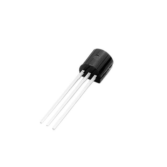
Dimensions – TO-92
A
TC Measuring Point
Dimension
A
B
Seating
Plane
C
Anode
Inches
Millimeters
Min
Max
Min
Max
0.175
0.205
4.450
5.200
0.210
4.320
5.330
B
0.170
C
0.500
D
0.135
E
0.125
0.165
3.180
4.190
F
0.080
0.105
2.040
2.660
G
0.016
0.021
0.407
0.533
H
0.045
0.055
1.150
1.390
I
0.095
0.105
2.420
2.660
J
0.015
0.020
0.380
0.500
12.70
3.430
Cathode
G
H
Gate
I
D
F
J
E
F
Packing Option
Part Number
Marking
Weight
Packing Mode
S8X5ECS
S8X5ECS
0.217G
Bulk
Base Quantity
2500
S8X5ECSRP
S8X5ECS
0.217G
Tape & Reel
2000
2000
S8X5ECSAP
S8X5ECS
0.217G
Ammo Pack
S8X5ECS2
S8X5ECS2
0.217G
Bulk
2500
S8X5ECS2RP
S8X5ECS2
0.217G
Tape & Reel
2000
S8X5ECS2AP
S8X5ECS2
0.217G
Ammo Pack
2000
© 2020 Littelfuse, Inc.
Specifications are subject to change without notice.
Revised: BO.12/08/20
�Thyristors
EV Series
Amp Sensitive
EV Series
0.5 Amp0.8Sensitive
SCRs SCRs
TO-92 (3-lead) Reel Pack (RP) Radial Leaded Specifications
0.02 (0.5 )
0.236
(6.0)
1.6
(41.0)
0.708
(18.0)
0.098 (2.5) MAX
1.2 6
(32.0)
0.354
(9.0)
0. 5
(12.7)
Gate
Cathode
0.2 (5.08)
Anode
0.1 (2.54)
0.157 DI A
(4.0)
14.17(360.0)
Flat up
1.9 7
(50.0)
Meets all EIA-468-C Standards
Dimensions
are in inches
(and millimeters).
Direction of Feed
TO-92 (3-lead) Ammo Pack (AP) Radial Leaded Specifications
0.236
(6.0 )
0.02 (0.5 )
0.098 (2.5) MAX
1.27
(32.2)
1.62
(41.2)
0.708
(18.0)
0.35 4
(9.0 )
0.1 (2.54)
0. 5
(12.7)
Cathode
0.2 (5.08)
0.157
(4.0 ) DI A
Gate
Anode
Flat down
n of Feed
Direc tio
25 Devices per fold
Meets all
EIA-468-C Standards
1.85
(47.0)
12. 2
(310.0 )
1.85
(47.0)
Dimensions
are in inche s
(and millimeters).
13. 3
(338.0)
Part Numbering System
Part Marking System
S 8X5 E C S xx
Series
S: SCR
Voltage
8: 800V
Current
X5: 0.5A
SOT89
Package Type
Blank: Bulk Pack
RP: Reel Pack
AP: Ammo Pack
Sesitivity & Type
S: 100µA Sensitive SCR
S2: 50µA Sensitive SCR
Package Type
EC: TO-92 Center Anode
SOT223
Line1 = Littelfuse Part Number
Line2 = continuation…Littelfuse Part Number
Y = Last Digit of Calendar Year
M = Letter Month Code (A-L for Jan-Dec)
L = Location Code
DD = Calendar Date
TO-92
Disclaimer Notice - Information furnished is believed to be accurate and reliable. However, users should independently evaluate the suitability of and test each product selected for their own applications. Littelfuse products are
not designed for, and may not be used in, all applications. Read complete Disclaimer Notice at http://www.littelfuse.com/disclaimer-electronics.
© 2020 Littelfuse, Inc.
Specifications are subject to change without notice.
Revised: BO.12/08/20
�
很抱歉,暂时无法提供与“S8X5ECSRP”相匹配的价格&库存,您可以联系我们找货
免费人工找货- 国内价格 香港价格
- 2000+2.294852000+0.29625
- 4000+2.109674000+0.27234
- 6000+2.024276000+0.26132
- 国内价格 香港价格
- 1+8.768451+1.13194
- 10+5.4805510+0.70750
- 100+3.58854100+0.46325
- 500+2.77666500+0.35845
- 1000+2.515011000+0.32467