TVS Diode Array (SPA® Diodes)
General Purpose ESD Protection - SP5003 Series
SP5003 Series 4 Channel Common Mode Filter
12/31/2020
RoHS Pb GREEN
ESU270-49
N/A
Description
The SP5003 Series is a highly integrated Common Mode
Filter (CMF) providing both ESD protection and EMI
common mode noise filtering for systems using high
speed differential serial interfaces, such as MIPI D-PHY or
HDMI.
The SP5003 Series can protect and filter two differential
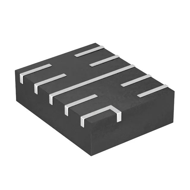
line pairs in a small RoHS-compliant TDFN-10 package, with
cost and space savings over discrete solutions.
Pinout
Features
10
1
• Large differential
bandwidth > 4.0 GHz
9
2
• High Common Mode
Stop Band Attenuation:
8
3
7
4
6
> 16 dB at 900 MHz
• Common Mode Imped
ance: Zc: 32Ω at 100 MHz
• TDFN-10 2.50mm ×
2.00mm × 0.75mm
package with 0.50mm
lead pitch
5
Note: Bottom-view
Functional Block Diagram
External
• RoHS-compliant, Leadfree packaging
• Moisture Sensitivity Level
(MSL-1)
Applications
Pin1
Pin10
Pin2
Pin9
Pin4
Pin7
Pin5
Pin6
(Connector)
Pin3
• ±15kV ESD protection
per channel (IEC 610004-2 Level 4, contact
discharge)
• HDMI/DVI Display in
Mobile Phones
Internal
(ASIC)
• MIPI D-PHY (CSI-2, DSI,
etc) in Mobile Phones and
Digital Still Cameras
Pin8
© 2021 Littelfuse, Inc.
Specifications are subject to change without notice.
Revised: 08/27/21
�TVS Diode Array (SPA® Diodes)
General Purpose ESD Protection - SP5003 Series
Absolute Maximum Ratings
Symbol
Parameter
Value
Units
IDC
DC Current Per Line
100
mA
PDC
DC Package Power Rating
0.5
Watts
TOP
Operating Temperature
-40 to 125
°C
TSTOR
Storage Temperature
-55 to 150
°C
CAUTION: Stresses above those listed in “Absolute Maximum Ratings” may cause permanent damage to the component. This is a stress only rating and operation of the component at these or any other conditions above those
indicated in the operational sections of this specification is not implied.
Electrical Characteristics (TOP=25ºC)
Parameter
Symbol
Test Conditions
RCH
Total Channel Capacitance
CTOTAL
Reverse Standoff Voltage
VRWM
Channel Resistance
Breakdown Voltage
Typ
Max
Units
Pins 1−10, 2−9, 4−7 and 5−6
3.5
5.0
Ω
VI/O = 1.65VDC Reverse Bias;
f=1MHz, 30mVAC
0.8
1.3
pF
5.0
V
8.0
10.0
V
VBR
Forward Voltage at IF
Min
IT=1mA
6.0
0.4
VF
IF=1mA
0.7
1.5
V
Reverse Leakage Current
ILEAK
VLeak=+3.3V
0.01
0.10
µA
Positive (tp=8/20µs)
1.36
Dynamic Resistance2 3
RDYN
Negative (tp=8/20µs)
0.6
TLP, tp=100ns, I/O to GND
Ω
0.42
IEC 61000-4-2 (Contact Discharge)
±15
kV
IEC 61000-4-2 (Air Discharge)
±30
kV
ESD Withstand Voltage1 2
VESD
Differential Mode Cutoff
Frequency2
F3dB
ZSOURCE=50 Ω, ZLOAD50 Ω
4.0
GHz
Common Mode Impedance
ZC
@100MHz
32
Ω
Common Mode Stop Band
Attenuation2
Fatten
f=900MHz
16
dB
Notes:
1. ESD zapping at I/O pins (1,2,4,5) with respect to GND.
2. Guaranteed by design.
3. Transmission Line Pulse (TLP) with 100ns width and 200ps rise time.
Differential Mode Attenuation vs. Frequency
Common Mode Attenuation vs. Frequency
0
0
−1
−5
−10
−3
Inser�on Loss(dB)
Inser�on Loss(dB)
−2
−4
−5
−6
−7
−15
−20
−25
−30
−8
−35
−9
−40
−10
1
10
100
Frequency (MHz)
1000
10000
1
10
100
1000
10000
Frequency (MHz)
© 2021 Littelfuse, Inc.
Specifications are subject to change without notice.
Revised: 08/27/21
�TVS Diode Array (SPA® Diodes)
General Purpose ESD Protection - SP5003 Series
Transmission Line Pulsing (TLP) Plot
22
20
18
TLP Current (A)
16
14
12
10
8
6
4
2
0
0
2
4
6
8
10
12
14
16
18
20
TLP Voltage (V)
Soldering Parameters
Pb – Free assembly
Pre Heat
- Temperature Min (Ts(min))
150°C
- Temperature Max (Ts(max))
200°C
- Time (min to max) (ts)
60 – 180 secs
Reflow
Critical Zone
TL to TP
Ramp-up
Average ramp up rate (Liquidus) Temp (TL) to peak 3°C/second max
3°C/second max
TS(max) to TL - Ramp-up Rate
tP
TP
- Temperature (TL) (Liquidus)
217°C
- Temperature (tL)
60 – 150 seconds
Peak Temperature (TP)
260
Time within 5°C of actual peak Temperature (tp)
20 – 40 seconds
Ramp-down Rate
6°C/second max
Time 25°C to peak Temperature (TP)
8 minutes Max.
Do not exceed
260°C
+0/-5
°C
Ordering Information
Temperature
Reflow Condition
TL
T S(max)
tL
Ramp-dow
Ramp-down
Preheat
T S(min)
tS
25
time to peak temperature
Time
Part Marking System
Part Number
Package
Size
Marking
SP5003-04TTG
TDFN-10
2.5x2.0mm
42***
Min. Order
Qty.
3000
Product Series
42 = SP5003
Part Numbering System
SP 5003
42 ***
–
04 T T G
TVS Diode Arrays
(SPA® Diodes )
Date Code
(Year / Week)
G= Green
T= Tape & Reel
Series
Number of Channels
04 = 4 Channel TDFN-10
Package
TDFN-10 (2.5x2.0mm)
© 2021 Littelfuse, Inc.
Specifications are subject to change without notice.
Revised: 08/27/21
�General Purpose ESD Protection - SP5003 Series
Package Dimensions —TDFN-10
D
0.10
TDFN-10
A B
L
2X
C
L
L1
PIN 1
MARKING
Symbol
Millimeters
DETAIL A
ALTERNATE TERMINAL
CONSTRUCTIONS
2X
JEDEC MO-229
E
C
0.10
0.05
C
TOP VIEW
DETAIL B
A3
C
A1
A1
DETAIL A
ALTERNATE
CONSTRUCTIONS
C
8X
PA C K A G E
O U T L INE
8X
1.07
5
0.30
8X L
0.10
MIN
Min
Max
A
0.70
0.80
0.028
0.031
A1
0.00
0.05
0.000
0.002
0.2 REF
0.15
b
DETAIL B
SIDE VIEW
1
Max
A3
A
0.05
A3
MOLD CMPD
EXPOSED Cu
Inches
Min
0.008 REF
0.25
0.006
0.010
D
2.50 BSC
0.098 BSC
E
2.00 BSC
0.079 BSC
e
0.50 BSC
0.020 BSC
L
0.70
0.90
0.028
0.035
L1
0.05
0.15
0.002
0.006
2.30
2
TVS Diode Array (SPA® Diodes)
1
10
e
6
0.45
9X b
0.10
M
C
0.05
M
C
A B
BOTTOM VIEW
0.50 P I T C H
Recommended
Soldering
Footprint
Tape & Reel Specification –TDFN-10
P0
T
P2
Φ 1.50 +0.10
E
Top
Cover
Tape
A0
F
W
5° Max
K0
B0
Φ 1.00 ±0.05
P
Φ 1.50 +0.10
Device Orientation
in Tape
Symbol
Dimensions
Millimetres
E
1.75+/- 0.10
F
3.5 +/- 0.05
P
4.0 +/- 0.10
P0
4.0 +/- 0.10
P2
2.0 +/- 0.05
W
8.00 +0.30/- 0.10
A0
Pin1 Location
2.19 +/- 0.05
B0
2.77 +/- 0.05
K0
1.05 +/- 0.05
T
0.25+/- 0.02
Device Orientation in Tape
E
F
Φ 1.00 ±0.05
Pin1 Location
Disclaimer Notice - Information furnished is believed to be accurate and reliable. However, users should independently evaluate the suitability of and test each product selected for their own applications. Littelfuse products are
not designed for, and may not be used in, all applications. Read complete Disclaimer Notice at http://www.littelfuse.com/disclaimer-electronics.
© 2021 Littelfuse, Inc.
Specifications are subject to change without notice.
Revised: 08/27/21
�
很抱歉,暂时无法提供与“SP5003-04TTG”相匹配的价格&库存,您可以联系我们找货
免费人工找货- 国内价格 香港价格
- 3000+3.508023000+0.45390