TVS Diode Arrays (SPA®® Diodes)
General Purpose ESD Protection - SP712
SP712 Series 640W Asymmetrical TVS Diode Array
RoHS
Pb GREEN
Description
The SP712 TVS Diode Array is designed to protect RS-485
applications with asymmetrical working voltages (-7V to
12V) from damage due to electrostatic discharge (ESD),
electrical fast transients (EFT), and lightning induced surges.
The SP712 can absorb repetitive ESD strikes above the
maximum level specified in IEC 61000-4-2 international
standard without performance degradation and safely
dissipate up to 20A of 8/20us induced surge current (IEC
61000-4-5) with very low clamping voltages.
Pinout and Functional Block Diagram
2
Features
1
12V
12V
7V
7V
• ESD, IEC 61000-4-2,
±30kV contact, ±30kV air
• Low clamping voltage
• EFT, IEC 61000-4-4, 50A
(5/50ns)
• Halogen free, Lead free
and RoHS compliant
• Lightning, IEC 610004-5 2nd edition, 20A
(tP=8/20μs)
• Moisture Sensitivity
Level(MSL -1)
• Working Voltages: -7V to
12V
• Low leakage current
• AEC-Q101 qualified
Applications
3
• RS-485
• Security Systems
• Fieldbus
• Modbus
• Automated Teller
Machines (ATMs)
• Profibus
• Lighting Control - DALI
• DMX512
• Communication
Equipments
RS-485 Application Example
RS-485 Port
Receiver
A
B
IC
SM712
SP712
GND
Life Support Note:
Not Intended for Use in Life Support or Life Saving Applications
The products shown herein are not designed for use in life sustaining or life saving
applications unless otherwise expressly indicated.
©2020 Littelfuse, Inc.
Specifications are subject to change without notice.
Revision: 01/13/20
�TVS Diode Arrays (SPA®® Diodes)
General Purpose ESD Protection - SP712
Absolute Maximum Ratings
Value
Units
PPk
Symbol
Peak Pulse Power (tp=8/20μs)
Parameter
640
W
IPP
Peak Pulse Current (tp=8/20μs)
20
A
TOP
Operating Temperature
-40 to 125
°C
TSTOR
Storage Temperature
-55 to 150
°C
Notes:
CAUTION: Stresses above those listed in “Absolute Maximum Ratings” may cause permanent damage to the component. This is a stress only rating and
operation of the component at these or any other conditions above those indicated in the operational sections of this specification is not implied.
Electrical Characteristics (TOP=25ºC)
Parameter
Symbol
Reverse Standoff Voltage
Test Conditions
VRWM
Breakdown Voltage
VC
Dynamic Resistance
12.0
V
9
V
IR=1mA, Pin 1 or Pin 2 to Pin 3
13.3
14.5
V
VR=7V
20
μA
VR=12V
1
μA
17
19
V
IPP=1A, tp=8/20µs, Pin 3 to Pin 1 or Pin 2
10
11
V
IPP=20A, tp=8/20µs, Pin 1 or Pin 2 to Pin 3
28
32
V
IPP=20A, tp=8/20µs, Pin 3 to Pin 1 or Pin 2
17
20
V
TLP, tP=100ns
0.26
Ω
IEC 61000-4-2 (Contact Discharge)
±30
kV
IEC 61000-4-2 (Air Discharge)
±30
kV
Reverse Bias=0V, f=1MHz;
Pin 1 or Pin 2 to Pin 3
CI/O-GND
Diode Capacitance1
V
IPP=1A, tp=8/20µs, Pin 1 or Pin 2 to Pin 3
VESD
ESD Withstand Voltage1
Units
7.0
7.5
RDYN
2
Max
IR=1mA, Pin 3 to Pin 1 or Pin 2
ILEAK
Clamp Voltage1
Typ
IR=1μA, Pin 1 or Pin 2 to Pin 3
VBR
Reverse Leakage
Current
Min
IR=1μA, Pin 3 to Pin 1 or Pin 2
75
pF
Notes : 1. Parameter is guaranteed by design and/or component characterization.
2 Transmission Line Pulse (TLP) test setting : Std.TDR(50Ω),tp=100ns, tr=0.2ns ITLP and VTLP averaging window: start t1=70ns to end t2=90ns
Clamping Voltage vs. IPP
80
35.0
70
30.0
Clamp Voltage-VC (V)
Capacitance (pF)
Capacitance vs. Reverse Bias
60
50
40
30
20
15.0
Pin3 to Pin1 or Pin2
10.0
0.0
0
2
4
6
Bias Voltage (V)
©2020 Littelfuse, Inc.
Specifications are subject to change without notice.
Revision: 01/13/20
20.0
5.0
10
0
Pin 1 or Pin 2 to Pin 3
25.0
8
10
12
0.0
5.0
10.0
15.0
Peak Pulse Current-IPP (A)
20.0
�TVS Diode Arrays (SPA®® Diodes)
General Purpose ESD Protection - SP712
Positive Transmission Line Pulsing (TLP) Plot
Negative Transmission Line Pulsing (TLP) Plot
0
25
-5
TLP Current (A)
TLP Current (A)
20
15
10
0
0
5
10
15
TLP Voltage (V)
20
25
IEC 61000-4-2 +8kV Contact ESD Clamping Voltage
8/20μs Pulse Waveform
110%
100%
90%
80%
Percent of IPP
-15
-20
5
70%
60%
50%
40%
30%
20%
10%
0%
-10
0.0
5.0
10.0
15.0
Time (μs)
©2020 Littelfuse, Inc.
Specifications are subject to change without notice.
Revision: 01/13/20
20.0
25.0
30.0
-25
-20
-15
-10
TLP Voltage (V)
-5
IEC 61000-4-2 -8kV Contact ESD Clamping Voltage
0
�TVS Diode Arrays (SPA®® Diodes)
General Purpose ESD Protection - SP712
Soldering Parameters
Pre Heat
Pb – Free assembly
- Temperature Min (Ts(min))
150°C
- Temperature Max (Ts(max))
200°C
- Time (min to max) (ts)
60 – 180 secs
Average ramp up rate (Liquidus) Temp (TL)
to peak
3°C/second max
TS(max) to TL - Ramp-up Rate
3°C/second max
Reflow
- Temperature (TL) (Liquidus)
217°C
- Temperature (tL)
60 – 150 seconds
260
Time within 5°C of actual peak
Temperature (tp)
20 – 40 seconds
Ramp-down Rate
6°C/second max
Time 25°C to peak Temperature (TP)
8 minutes Max.
Do not exceed
260°C
Critical Zone
TL to TP
Ramp-up
TL
TS(max)
tL
Ramp-do
Ramp-down
Preheat
TS(min)
25
Peak Temperature (TP)
+0/-5
tP
TP
Temperature
Reflow Condition
tS
time to peak temperature
Time
°C
Part Marking System
Product Characteristics
Lead Plating
Matte Tin
Lead Material
Copper Alloy
Lead Coplanarity
0.004 inches(0.102mm)
Substrate Material
Silicon
Body Material
Molded Compound
Flammability
UL Recognized compound meeting
flammability rating V-0
AEFD
AE : Part code
F : Assembly code
D : Date code
Ordering Information
Part Numbering System
Part Number
Package
SP712-02HTG
SOT23-3L
Min. Order Qty.
3000
SP 712 – 02 H T G
TVS Diode Arrays
(SPA® Diodes)
Series
Working
Voltage
Number of
Channels
©2020 Littelfuse, Inc.
Specifications are subject to change without notice.
Revision: 01/13/20
G= Green
T= Tape & Reel
Package
H: SOT23-3L
�TVS Diode Arrays (SPA®® Diodes)
General Purpose ESD Protection - SP712
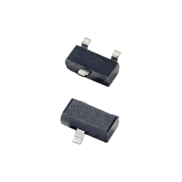
Package Dimensions — SOT23-3
Package
Pins
JEDEC
L1 (Guage Plan)
Pin1
E
E1
D
A
A1
b
c
D
E
E1
e
e1
L
L1
θ
bx3
e
θ
e1
L
Top View
Detail A
Side View
Side View
c
A1
A
Detail A
SOT23-3
3
TO-236
Millimeters
Min
Max
0.90
1.15
0.00
0.10
0.30
0.51
0.08
0.20
2.80
3.04
2.10
2.64
1.20
1.40
0.95 BSC
1.90 BSC
0.30
0.55
0.25 BSC
0°
8°
Inches
Min
Max
0.035
0.045
0.000
0.004
0.012
0.020
0.003
0.008
0.110
0.120
0.083
0.104
0.047
0.055
0.038 BSC
0.075 BSC
0.012
0.022
0.010 BSC
0°
8°
Millimeters
Inches
2.90
0.80
1.30
0.60
1.30
2.50
Recommended soldering pad layout (unit :mm)
Drawing# : H03-B
Embossed Carrier Tape & Reel Specification — SOT23-3
Symbol
8mm TAPE AND REEL
GENERAL INFORMATION
1. 3000 PIECES PER REEL.
2. ORDER IN MULTIPLES OF FULL REELS ONLY.
3. MEETS EIA-481 REVISION "A" SPECIFICATIONS.
ACCESS HOLE
14.4mm
SOT23-3 (8mm POCKET PITCH)
13mm
180mm
60mm
USER DIRECTION OF FEED
Min
Max
Min
Max
E
1.65
1.85
0.065
0.073
F
3.40
3.60
0.134
0.142
P2
1.90
2.10
0.075
0.083
D
1.40
1.60
0.055
0.063
P0
3.90
4.10
0.154
0.161
W
7.70
8.30
0.303
0.327
P
3.90
4.10
0.154
0.161
A0
3.05
3.25
0.120
0.128
B0
2.67
2.87
0.105
0.113
K0
1.12
1.32
0.044
0.052
t
0.22
0.24
0.009
0.009
PIN 1
8.4mm
Disclaimer Notice - Information furnished is believed to be accurate and reliable. However, users should independently evaluate the suitability of and
test each product selected for their own applications. Littelfuse products are not designed for, and may not be used in, all applications.
Read complete Disclaimer Notice at http://www.littelfuse.com/disclaimer-electronics.
©2020 Littelfuse, Inc.
Specifications are subject to change without notice.
Revision: 01/13/20
COVER TAPE
�
很抱歉,暂时无法提供与“SP712-02HTG”相匹配的价格&库存,您可以联系我们找货
免费人工找货