Thyristors Datasheet
SVxx12xx series
12 Amp High Junction Temperature SCRs
RoHS
Description
The SVxx12xx high junction temperature SCR series is ideal for
uni-directional switch applications such as phase control in heating,
motor speed controls, converters/rectifiers, inrush current control
and capacitive discharge ignitions.
These SCRs have a low gate current, (IGT) trigger level of 6mA
and 10mA maximum at approximately 1.5V for SVxx12x1 and
SVxx12x2, respectively.
Features & Benefits
■ �Halogen free and RoHS
compliant
■ 150°C maximum junction
temperature
Agency File Number
Applications
L Packages: E71639
Typical applications include AC Generator (ACG) rectifiers, battery
voltage regulators and generic converters and inrush current
controller in various AC to DC applications. Additional applications
include controls for power tools, home/brown good and white
goods appliances.
Internally constructed isolated packages offered for ease of heat
sinking with high isolation voltage.
Main Features
Symbol
■ Recognized to UL 1557 as an
Electrically Semiconductor
Device
■ Surge capability up to 120A at
60Hz half cycle
Agency Approval
Agency
■ �High dv/dt performance
Value
Unit
A
IT(RMS)
12
VDRM /VRRM
600
V
IGT
6 to 10
mA
Schematic Symbol
A
K
G
1
© 2021 Littelfuse, Inc.
Specifications are subject to change without notice.
Revised: GD.06/16/21
�Thyristors Datasheet
SVxx12xx series
12 Amp High Junction Temperature SCRs
Absolute Maximum Ratings
Symbol
Parameter
Test Conditions
Value
Unit
VDSM/VRSM
Peak non-repetitive blocking voltage
PW=100 μs
800
V
IT(RMS)
RMS on-state current
12
A
IT(AV)
Average on-state current
7.6
A
ITSM
Peak non-repetitive surge current
(single half cycle, TJ (initial) = 25°C)
f = 50Hz
100
f = 60Hz
120
I2t
I2t Value for fusing
tp = 8.3 ms
60
A2s
di/dt
Critical rate of rise of on-state current
f = 60Hz; TJ = 150°C
100
A/μs
IGM
Peak gate current
TJ = 150°C
4
A
PG(AV)
Average gate power dissipation
TJ = 150°C
0.8
W
Tstg
Storage temperature range
-40 to 150
TJ
Operating junction temperature range
-40 to 150
SVxx12Lx
SVxx12Rx
SVxx12Nx
SVxx12Lx
SVxx12Rx
SVxx12Nx
TC = 110°C
TC = 135°C
TC = 110°C
TC = 135°C
A
°C
Note: xx=voltage/10, x=sensitivity
Electrical Characteristics (TJ = 25°C, unless otherwise specified)
Symbol
Test Conditions
IGT
VD = 12V RL = 60 Ω
dv/dt
SVxx12x1
SVxx12x2
MAX.
6
10
MIN.
2
5
400
800
200
400
VD = 67% VDRM; gate open; TJ = 125°C
MIN.
VD = 67% VDRM; gate open; TJ = 150°C
Unit
mA
V/μs
VGD
VD = VDRM RL = 3.3 kΩ TJ = 150°C
MIN.
0.2
0.2
V
IH
IT = 200mA (initial)
MAX.
22
35
mA
tq
IT = 2A; tp = 50µs; dv/dt = 5V/µs; di/dt = 30A/µs
MAX.
25
25
μs
tgt
IG = 2 x IGT PW = 15µs IT = 24A
TYP.
2.6
2.6
μs
Note: xx=voltage/10, x=package
Static Characteristics
Symbol
Test Conditions
VTM
IT = 24A; tp = 380 µs
MAX.
TJ = 25°C
IDRM / IRRM
VDRM = VRRM
Value
Unit
1.6
V
10
MAX.
TJ = 125°C
TJ = 150°C
μA
500
2000
Thermal Resistances
Symbol
RƟ(JC)
Parameter
Junction to case (AC)
Value
SVxx12Lx
SVxx12Rx
SVxx12Nx
2.5
1.1
Unit
°C/W
Note: xx=voltage/10, x=package
2
© 2021 Littelfuse, Inc.
Specifications are subject to change without notice.
Revised: GD.06/16/21
�Thyristors Datasheet
SVxx12xx series
12 Amp High Junction Temperature SCRs
Figure 1:
Normalized DC Gate Trigger Current
vs. Junction Temperature
Figure 2:
Normalized DC Gate Trigger Voltage
vs. Junction Temperature
1.4
2.0
1.8
1.2
Ratio of VGT/VGT(TJ=25˚C)
Ratio of IGT/IGT(TJ=25˚C)
1.6
1.4
1.2
1.0
0.8
0.6
1.0
0.8
0.6
0.4
0.4
0.2
0.2
0.0
-40
-15
10
35
60
85
110
Junction Temperature (TJ)- ºC
135
0.0
150
Figure 3:
Normalized DC Holding Current vs. Junction Temperature
30
Instantaneous On-State Current(IT) -Amps
1.8
Ratio of IH/IH(TJ=25˚C)
1.6
1.4
1.2
1.0
0.8
0.6
0.4
0.2
-40
-15
10
35
60
85
110
Junction Temperature (TJ)- ºC
135
-15
10
35
60
85
110
Junction Temperature (TJ)- ºC
TJ=25º
20
15
10
5
0
150
0.7
0.8
0.9
1
1.1
1.2
1.3
Instantaneous On-State Voltage(VT) -Volts
1.4
1.5
Figure 6:
Maximum Allowable Case Temperature
vs. RMS On-State Current
25
150
SVxx12Rx
SVxx12Nx
140
20
Maximum Allowable
Case Temperature (TC)- °C
Average On-State
Power Dissipation (PD(AV))-Watts
150
25
Figure 5:
Power Dissipation (Typical) vs. RMS On-State Current
15
10
5
130
SVxx12Lx
120
110
100
90
80
0
135
Figure 4:
On-State Current vs. On-State Voltage (Typical)
2.0
0.0
-40
0
5
10
15
RMS On-State Current (IT(RMS))
- Amps
20
CURRENT WAVEFORM: Sinusoidal
LOAD: Resistive or Inductive
CONDUCTION ANGLE: 180°
0
2
4
6
8
10
12
14
RMS On-State Current [IT(RMS)] - Amps
3
© 2021 Littelfuse, Inc.
Specifications are subject to change without notice.
Revised: GD.06/16/21
�Thyristors Datasheet
SVxx12xx series
12 Amp High Junction Temperature SCRs
Figure 7:
Maximum Allowable Case Temperature
vs. Average On-State Current
Figure 8:
Peak Capacitor Discharge Current
1000
150
Peak Discharge Current (ITM) - Amps
SVxx12Rx
SVxx12Nx
Maximum Allowable Case
Temperature (TC) - °C
140
130
120
SVxx12Lx
110
100
CURRENT WAVEFORM: Sinusoidal
LOAD: Resistive or Inductive
CONDUCTION ANGLE: 180°
90
80
0
1
2
3
SJxx16Dx
SJxx16Vx
4
5
6
7
100
ITRM
tW
8
10
05
.
Average On-State Current [IT(AVE)] - Amps
5 .0
25.0
50.0
Pulse Current Duration (tw) - ms
Figure 9:
Peak Capacitor Discharge Current Derating
1.2
Normalized Peak Current
1.0
0.8
0.6
0.4
0.2
0.0
0
25
50
75
100
125
150
Case Temperature (TC) - ºC
Figure 10: Surge Peak On-State Current vs. Number of Cycles
Peak Surge (Non-repetitive)
On-state Current (ITSM ) – Amps
1000
SUPPLY FREQUENCY: 60 Hz Sinusoidal
LOAD: Resistive
RMS On-State Current: [IT(RMS)]: Maximum Rated
Value at Specified Case Temperature
Notes:
1. G
� ate control may be lost during and immediately
following surge current interval.
2. O
� verload may not be repeated until junction
temperature has returned to steady-state
rated value.
100
10
1
1
10
10 0
10 0 0
Surge Current Duration - Full Cycles
4
© 2021 Littelfuse, Inc.
Specifications are subject to change without notice.
Revised: GD.06/16/21
�Thyristors Datasheet
SVxx12xx series
12 Amp High Junction Temperature SCRs
Soldering Parameters
Pb – Free assembly
Pre Heat
- Temperature Min (Ts(min))
150°C
- Temperature Max (Ts(max))
200°C
- Time (min to max) (ts)
Average ramp up rate (Liquidus Temp) (TL) to
peak
TS(max) to TL - Ramp-up Rate
Reflow
Ramp-up
60 – 180 secs
5°C/second max
5°C/second max
- Temperature (TL) (Liquidus)
217°C
- Time (tL)
60 – 150 seconds
Peak Temperature (TP)
260
Time within 5°C of actual peak Temperature (tp)
20 – 40 seconds
Ramp-down Rate
5°C/second max
Time 25°C to peak Temperature (TP)
8 minutes Max.
Do not exceed
280°C
+0/-5
TL
Body Material
Lead Material
tL
T S(max)
Preheat
T S(min)
Ramp-dow
Ramp-down
tS
°C
25
time to peak temperature
Physical Specifications
Terminal Finish
tP
TP
Temperature
Reflow Condition
Time
Environmental Specifications
100% Matte Tin-plated
UL Recognized compound meeting flammability
rating V-0
Copper Alloy
Test
AC Blocking
Temperature Cycling
Design Considerations
Careful selection of the correct component for the application’s
operating parameters and environment will go a long way toward
extending the operating life of the Thyristor. Good design practice
should limit the maximum continuous current through the main
terminals to 75% of the component rating. Other ways to ensure
long life for a power discrete semiconductor are proper heat
sinking and selection of voltage ratings for worst case conditions.
Overheating, overvoltage (including dv/dt), and surge currents are
the main killers of semiconductors. Correct mounting, soldering,
and forming of the leads also help protect against component
damage.
Temperature/Humidity
Resistance to Solder Heat
Solderability
Lead Bend
Moisture Sensitivity Level
5
Specifications and Conditions
MIL-STD-750, M-1040, Cond A
Applied Peak AC voltage @ 150°C for
1008 hours
MIL-STD-750, M-1051,
1000 cycles; -55°C to +150°C;
15-min dwell-time
EIA / JEDEC, JESD22-A101
1008 hours; 160V - DC: 85°C;
85% rel humidity
MIL-STD-750 Method 2031
ANSI/J-STD-002, category 3, Test A
MIL-STD-750, M-2036 Cond E
Level 1, JEDEC-J-STD-020D
© 2021 Littelfuse, Inc.
Specifications are subject to change without notice.
Revised: GD.06/16/21
�Thyristors Datasheet
SVxx12xx series
12 Amp High Junction Temperature SCRs
Dimensions — TO-220AB (L-Package) — Isolated Mounting Tab
TC MEASURING POINT
O
A
E
P
AREA (REF.) 0.17 IN2
Dimension
8.13
.320
A
B
C
D
E
F
G
H
J
K
L
M
N
O
P
R
B
C
13.36
.526
D
7.01
.276
F
R
G
L
H
CATHODE
ANODE
GATE
N
K
M
J
Inches
Millimeters
Min
Max
Min
Max
0.380
0.105
0.230
0.590
0.142
0.110
0.540
0.025
0.195
0.095
0.060
0.085
0.018
0.178
0.045
0.038
0.420
0.115
0.250
0.620
0.147
0.130
0.575
0.035
0.205
0.105
0.075
0.095
0.024
0.188
0.060
0.048
9.65
2.67
5.84
14.99
3.61
2.79
13.72
0.64
4.95
2.41
1.52
2.16
0.46
4.52
1.14
0.97
10.67
2.92
6.35
15.75
3.73
3.30
14.61
0.89
5.21
2.67
1.91
2.41
0.61
4.78
1.52
1.22
Dimensions — TO-220AB (R-Package) — Non-Isolated Mounting Tab Common with
Center Lead
TC MEASURING POINT
O
A
E
P
AREA (REF.) 0.17 IN2
Dimension
8.13
.320
A
B
C
D
E
F
G
H
J
K
L
M
N
O
P
R
ANODE
B
C
13.36
.526
D
7.01
.276
NOTCH IN
GATE LEAD
TO ID.
NON-ISOLATED
TAB
F
R
G
L
H
CATHODE
ANODE
K
J
GATE
N
M
Note: Maximum torque to be applied to mounting
tab is 8 in-lbs. (0.904 Nm).
6
Inches
Millimeters
Min
Max
Min
Max
0.380
0.105
0.230
0.590
0.142
0.110
0.540
0.025
0.195
0.095
0.060
0.085
0.018
0.178
0.045
0.038
0.420
0.115
0.250
0.620
0.147
0.130
0.575
0.035
0.205
0.105
0.075
0.095
0.024
0.188
0.060
0.048
9.65
2.67
5.84
14.99
3.61
2.79
13.72
0.64
4.95
2.41
1.52
2.16
0.46
4.52
1.14
0.97
10.67
2.92
6.35
15.75
3.73
3.30
14.61
0.89
5.21
2.67
1.91
2.41
0.61
4.78
1.52
1.22
© 2021 Littelfuse, Inc.
Specifications are subject to change without notice.
Revised: GD.06/16/21
�Thyristors Datasheet
SVxx12xx series
12 Amp High Junction Temperature SCRs
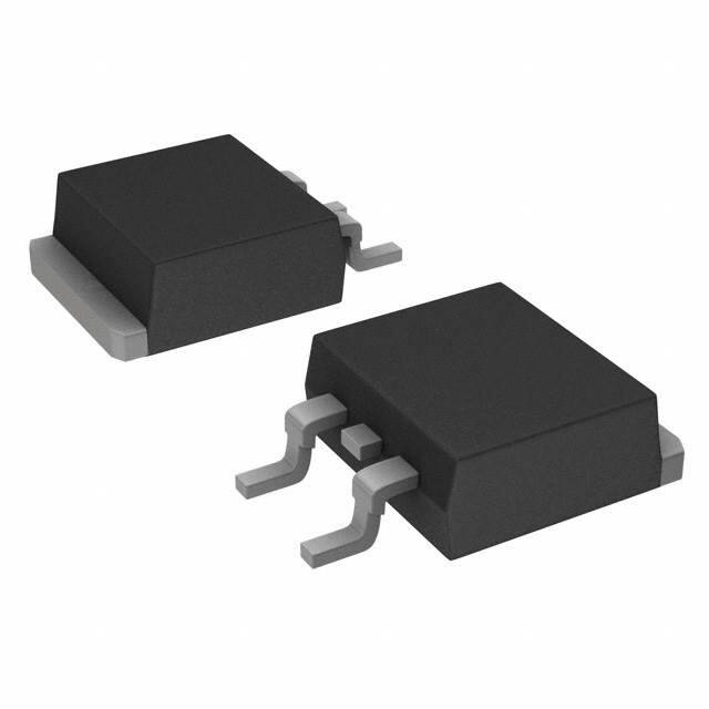
Dimensions — TO- 263AB (N-package) — D2-Pak Surface Mount
TC MEASURING POINT
B
AREA: 0.11 in
C
V
2
Dimension
E
ANODE
A
B
C
D
E
F
G
H
J
K
S
V
U
W
8.41
.331
7.01
.276
A
S
W
U
K
GATE
CATHODE
G
J
8.13
.320
H
D
F
11.68
.460
2.16
.085
7.01
.276
7.01
.276
Inches
Millimeters
Min
Max
Min
Max
0.360
0.380
0.178
0.025
0.045
0.060
0.095
0.092
0.018
0.090
0.590
0.035
0.002
0.040
0.370
0.420
0.188
0.035
0.060
0.075
0.105
0.102
0.024
0.110
0.625
0.045
0.010
0.070
9.14
9.65
4.52
0.64
1.14
1.52
2.41
2.34
0.46
2.29
14.99
0.89
0.05
1.02
9.40
10.67
4.78
0.89
1.52
1.91
2.67
2.59
0.61
2.79
15.88
1.14
0.25
1.78
16.89
.665
8.89
.350
1.40
.055
3.81
.150
2.03
.080
6.60
.260
Product Selector
Part Number
SVxx12L1
SVxx12R1
SVxx12N1
SVxx12L2
SVxx12R2
SVxx12N2
Voltage
600V
X
X
X
X
X
X
Gate Sensitivity
Type
Package
6mA
6mA
6mA
10mA
10mA
10mA
Standard SCR
Standard SCR
Standard SCR
Standard SCR
Standard SCR
Standard SCR
TO-220L
TO-220R
TO-263
TO-220L
TO-220R
TO-263
Note: xx = Voltage/10
Packing Options
Part Number
Marking
Weight
Packing Mode
Base Quantity
SVxx12LxTP
SVxx12RxTP
SVxx12NxTP
SVxx12NxRP
SVxx12Ly
SVxx12Ry
SVxx12Ny
SVxx12Ny
2.2g
2.2g
1.6g
1.6g
Tube
Tube
Tube
Embossed Carrier
1000 (50 per tube)
1000 (50 per tube)
1000 (50 per tube)
500
Note: xx=voltage/10, x=sensitivity
7
© 2021 Littelfuse, Inc.
Specifications are subject to change without notice.
Revised: GD.06/16/21
�Thyristors Datasheet
SVxx12xx series
12 Amp High Junction Temperature SCRs
Part Numbering System
Part Marking System
T0-220 AB - (L and R Package)
T0-263 AB - (N Package)
SV 60 12 R 1 TP
Packing Type
TP: Tube Pack
RP: Reel Pack
Component Type
SV: high temperature
high dv/dt SCR
SV6012L1
YM
Sensitivity & Type
1: 6mA
2:10mA
Voltage Rating
60: 600V
®
Package Type
L: TO-220 Isolated
R: TO-220 Non-Isolated
N: TO-263 (D2-Pak)
Current Rating
12: 12A
Date Code Marking
Y:Year Code
M: Month Code
XXX: Lot Trace Code
TO-263 Embossed Carrier Reel Pack (RP) Specifications
Meets all EIA-481-2 Standards
0.63
(16.0)
0.157
(4.0)
Gate
0.059
DI A
(1.5)
0.945
(24.0)
0.827
(21.0)
Cathode
*
* Co ver tape
Anode
0.512 (13.0) Arbor
Hole Dia.
12.99
(330.0)
Dimensions
are in inches
(and millimeters).
1.01
(25.7)
Direction of F eed
Disclaimer Notice - Information furnished is believed to be accurate and reliable. However, users should independently evaluate the suitability of and test each product selected for their own applications. Littelfuse products are
not designed for, and may not be used in, all applications. Read complete Disclaimer Notice at http://www.littelfuse.com/disclaimer-electronics.
8
© 2021 Littelfuse, Inc.
Specifications are subject to change without notice.
Revised: GD.06/16/21
�
很抱歉,暂时无法提供与“SV6012N1QRP”相匹配的价格&库存,您可以联系我们找货
免费人工找货- 国内价格
- 1+3.20534
- 200+1.24049
- 500+1.19686
- 1000+1.17537