Metal-Oxide Varistors (MOVs)
Surface Mount Varistors > SM7 Series
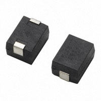
SM7 Varistor Series
RoHS
Description
The Littelfuse SM7 is a plastic-encapsulated surface
mount MOV in a PPS material molded package with
tin-plated terminal which is fully qualified in lead free
soldering and available for both reflow and wave
soldering process. SM7 is constructed with 7mm
varistor element disc. Its maximum operating ambient
temperature is 85ºC with peak pulse current of 1200A.
Features
Agency Approvals
Agency
Agency Approval
Agency File Number
UL1449
E320116
• Electrical equivalent
to leaded types
LA/ZA series
• Good solderability
• AC Voltage Rating
50 to 510VAC rms
• Application of AC
power meters
• No De-Rating up
to 85°C ambient
• Lead free and
RoHS compliant
• Available in tape
and reel
Additional Information
Datasheet
Samples
Resources
Absolute Maximum Ratings
• For ratings of individual members of a series, see Device Ratings and Specifications chart
Continuous
SM7 Series
Units
AC Voltage Range (VM(AC)RMS)
50 to 510
V
DC Voltage Range (VM(DC))
68 to 675
V
1200
A
Steady State Applied Voltage:
Transients:
Peak Pulse Current (ITM)
For 8/20µs Current Wave (See Figure 2)
Single Pulse Energy Range
For 10/1000µs Current Wave (WTM)
10 to 40
J
Operating Ambient Temperature Range (TA)
-40 to +85
O
Storage Temperature Range (TSTG)
-40 to +125
O
Temperature Coefficient (aV) of Clamping Voltage (VC) at Specified Test Current
Hi-Pot Encapsulation (COATING Isolation Voltage Capability)
(Dielectric must withstand indicated DC voltage for one minute per MIL-STD 202, Method 301)
COATING Insulation Resistance
SM7 Series
SM7 Series Ratings & Specifications
Maximum Rating (85°C)
Continuous
Transient
Part
Number
V50SM7
V60SM7
V115SM7
V130SM7
V140SM7
V150SM7
V175SM7
V230SM7
V250SM7
V275SM7
V300SM7
V320SM7
V385SM7
V420SM7
V460SM7
V480SM7
V510SM7
Specifications (25°C)
Peak Current
8 x 20µs
Typical
Capacitance
f = 1MHz
VDC
Energy
10 x 1000µs
VM(AC)
VM(DC)
WTM
ITM
VNOM Min
VNOM Max
VC
IPK
C
(V)
(V)
(J)
(A)
(V)
(V)
(V)
(A)
(pF)
50
60
115
130
140
150
175
230
250
275
300
320
385
420
460
480
510
68
81
153
175
180
200
225
300
330
369
405
420
505
560
615
640
675
4
5
10
11
12
13
15
20
21
23
25
25
27
30
37
35
40
1200
1200
1200
1200
1200
1200
1200
1200
1200
1200
1200
1200
1200
1200
1200
1200
1200
73
90
162
184
198
212
247
324
354
389
420
462
558
610
640
670
735
91
110
198
228
242
268
303
396
429
473
517
565
682
748
790
825
910
135
165
300
340
360
395
455
595
650
710
775
850
1025
1120
1190
1240
1200
10
10
10
10
10
10
10
10
10
10
10
10
10
10
10
10
10
700
600
200
180
160
150
130
100
90
80
70
65
60
55
55
50
45
11.4±0.3
Part Numbering System
V 275 SM7
8.3±0.3
0.3 max
3.6+/-0.3 for
V50SM7-V60SM7
6.0+/-0.3 for
V115SM7 to V510SM7
3.0±0.3
1.5±0.3
13.1
Maximum Clamping
Voltage
8 x 20 µs
VRMS
Product Dimensions
6.5
Varistor Voltage
at 1mA DC
Test Current
3.5
All dimensions shown
in milimeters
For “VARISTOR”
V M(AC)
(Three digits -- 115V to 510V)
SM7 SERIES
Soldering Pad Layout
© 2020 Littelfuse, Inc.
Specifications are subject to change without notice.
Revised: 09/09/20
�Metal-Oxide Varistors (MOVs)
Surface Mount Varistors > SM7 Series
Lead (Pb) Soldering Recommendations
Wave soldering is the most strenuous of the processes.
To avoid the possibility of generating stresses due to
thermal shock, a preheat stage in the soldering process
is recommended, and the peak temperature of the solder
process should be rigidly controlled.
When using a reflow process, care should be taken to
ensure that the SM7 chip is not subjected to a thermal
gradient steeper than 4 degrees per second; the ideal
gradient being 2 degrees per second. During the soldering
process, preheating to within 100 degrees of the solder's
peak temperature is essential to minimize thermal shock.
Once the soldering process has been completed, it is
still necessary to ensure that any further thermal shocks
are avoided. One possible cause of thermal shock is hot
printed circuit boards being removed from the solder
process and subjected to cleaning solvents at room
temperature. The boards must be allowed to cool gradually
to less than 50ºC before cleaning.
250
MAXIMUM TEMPERATURE
230°C
200
250
TEMPERATURE
°C
TEMPERATURE
°C
The terminals of SM7 series devices are tin plated copper,
and the recommended solder is 62/36/2 (Sn/Pb/Ag), 60/40
(Sn/Pb) or 63/37 (Sn/Pb). Littelfuse also recommends an
RMA solder flux.
Reflow Solder Profile
40-80
MAXIMUM TEMPERATURE
SECONDS
230°C
ABOVE 183°C
150
200
RAMP RATE 40-80
SECONDS
SM7 Series
Tape & Reel Specifications for V50SM7 amd V60SM7
Carrier Tape
P0
P1
E
D0
P2
B
5°
P1
T
A0
11.30
B-B
E
15°
D1
B
ier Tape
3.60
B0
W
A
F
A
5°
T
16.00±0.30
0.40±0.05
11.80±0.10
8.60±0.10
4.80±0.10
1.75±0.10
7.50±0.10
4.00±0.10
16.00±0.10
2.00±0.10
ø1.50 +0.10/-0
ø1.50 +0.10/-0
3.60
3.8 - 4.0mm
B0
W
D1
A-A
B
mm
W
T
A0
B0
K0
E
F
P0
P1
P2
D0
D1
NOTES:
1) All dimensions per EIA-481-c
2) 10 pitches cumulative tolerance on tape ±0.20mm
3) Quantity per 13 inch (330 mm) reel: 600 pcs
K0
F
2
B
Part
B-B
Plastic Reel
2±0.5
0.2
3±
Ø1
K0
DETAIL H
0.8
Ø330
Ø100
Ø21±
R1
16.5
120°
tic Reel
21.5±0.4
DETAIL H DETAIL H
0.2
3±
Ø1
2±0.5
Ø330
R1
Carrier Tape
P0
W
16.00±0.30
T
0.40±0.05
A0
11.80±0.10
B0
8.60±0.10
K0
6.80±0.10
E
1.75±0.10
D1
B
3.60
B0
W
5°
B
A
T
A0
11.30
B-B
5°
6.2
K0
2
10°
mm
E
D0
21.5±0.4
A
Part
P1
P2
120°
F
16.5
A-A
F
7.50±0.10
P0
4.00±0.10
P1
16.00±0.10
P2
2.00±0.10
D0
ø1.50 +0.10/-0
D1
ø1.50 +0.10/-0
NOTES:
1) All dimensions per EIA-481-c
2) 10 pitches cumulative tolerance on tape ±0.20mm
3) Quantity per 13 inch (330 mm) reel: 600 pcs
Plastic Reel
DETAIL H
0.2
3±
Ø1
2±0.5
0.8
Ø100
Ø21±
Ø330
Ø100
0.8
Tape & Reel Specifications
for V115SM7 to V510SM7
Ø21±
R1
16.5
120°
DETAIL H
21.5±0.4
Disclaimer Notice - Information furnished is believed to be accurate and reliable. However, users should independently evaluate the suitability of and test each product selected for their own applications. Littelfuse products are
not designed for, and may not be used in, all applications. Read complete Disclaimer Notice at www.littelfuse.com/disclaimer-electronics.
© 2020 Littelfuse, Inc.
Specifications are subject to change without notice.
Revised: 09/09/20
�