HMC-ALH445
v03.0410
GaAs HEMT MMIC LOW NOISE AMPLIFIER, 18 - 40 GHz
Features
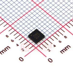
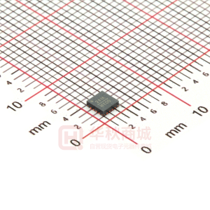
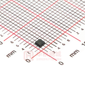
Noise Figure: 3.9 dB @ 28 GHz Gain: 9 dB P1dB Output Power: +12 dBm @ 28 GHz Supply Voltage: +5V @ 45 mA Die Size: 1.6 x 1.6 x 0.1 mm
1
AMPLIFIERS - LOW NOISE - CHIP
Typical Applications
This HMC-ALH445 is ideal for: • Wideband Communication Systems • Point-to-Point Radios • Point-to-Multi-Point Radios • Military & Space • Test Instrumentation
Functional Diagram
General Description
The HMC-ALH445 is a GaAs MMIC HEMT self-biased, wideband Low Noise Amplifier die which operates between 18 and 40 GHz. The amplifier provides 9 dB of gain, 3.9 dB noise figure at 28 GHz and +12 dBm of output power at 1 dB gain compression while requiring only 45 mA from a single +5V supply. The HMC-ALH445 amplifier is ideal for integration into Multi-Chip-Modules (MCMs) due to its small size.
Electrical Specifi cations*, TA = +25° C, Vdd= +5V
Parameter Frequency Range Gain Noise Figure Input Return Loss Output Return Loss Output Power for 1 dB Compression Supply Current (Idd) (Vdd = 5V) *Unless otherwise indicated, all measurements are from probed die 8 Min. Typ. 18 - 28 9 4 10 15 12 45 5 8 Max. Min. Typ. 28 - 40 10 3.9 10 15 13 45 4.5 Max. Units GHz dB dB dB dB dBm mA
1 - 192
For price, delivery and to place orders: Hittite Microwave Corporation, 20 Alpha Road, Chelmsford, MA 01824 Phone: 978-250-3343 Fax: 978-250-3373 Order On-line at www.hittite.com Application Support: Phone: 978-250-3343 or apps@hittite.com
�HMC-ALH445
v03.0410
GaAs HEMT MMIC LOW NOISE AMPLIFIER, 18 - 40 GHz
Gain vs. Temperature
14
Broadband Gain vs. Return Loss
15 10
1
AMPLIFIERS - LOW NOISE - CHIP
1 - 193
12 RESPONSE (dB)
5 0 -5 -10 -15 -20 -25 -30 18 20 22 24 26 28 30 32 34 FREQUENCY (GHz) 36 38 40 10 15 20 25 30 35 FREQUENCY (GHz) 40 45 50
S21 S11 S22
GAIN (dB)
10
8
+25C +85C - 55C
6
4
Input Return Loss vs. Frequency
-10
Output Return Loss vs. Frequency
-10
-15 RETURN LOSS (dB) RETURN LOSS (dB)
-15
-20
-20
+25C +85C - 55C
-25
+25C +85C - 55C
-25
-30
-30
-35 18 20 22 24 26 28 30 32 34 FREQUENCY (GHz) 36 38 40
-35 18 20 22 24 26 28 30 32 34 FREQUENCY (GHz) 36 38 40
Reverse Isolation vs. Temperature
-10
+25C +85C - 55C
Noise Figure vs. Frequency
RETURN LOSS (dB)
-15
-20
-25
-30 18 20 22 24 26 28 30 32 34 FREQUENCY (GHz) 36 38 40
Note: Measured Performance Characteristics (Typical Performance at 25°C) Vd1 = 5V, Id1 = 45 mA
For price, delivery and to place orders: Hittite Microwave Corporation, 20 Alpha Road, Chelmsford, MA 01824 Phone: 978-250-3343 Fax: 978-250-3373 Order On-line at www.hittite.com Application Support: Phone: 978-250-3343 or apps@hittite.com
�HMC-ALH445
v03.0410
GaAs HEMT MMIC LOW NOISE AMPLIFIER, 18 - 40 GHz
1
AMPLIFIERS - LOW NOISE - CHIP
On-Wafer P1dB vs. Frequency
Absolute Maximum Ratings
Drain Bias Voltage Drain Bias Current RF Input Power Thermal Resistance (channel to die bottom) Channel Temperature Storage Temperature Operating Temperature +5.5 Vdc 60 mA 10 dBm 201.2 °C/W 180 °C -65 to +150 °C -55 to +85 °C
ELECTROSTATIC SENSITIVE DEVICE OBSERVE HANDLING PRECAUTIONS
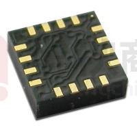
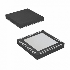
Outline Drawing
Die Packaging Information [1]
Standard GP-1 (Gel Pack) Alternate [2]
NOTES: 1. ALL DIMENSIONS ARE IN INCHES [MM]. 2. TYPICAL BOND PAD IS .004” SQUARE. 3. BACKSIDE METALLIZATION: GOLD. 4. BACKSIDE METAL IS GROUND. 5. BOND PAD METALLIZATION: GOLD. 6. CONNECTION NOT REQUIRED FOR UNLABELED BOND PADS. 7. OVERALL DIE SIZE ±.002”
[1] Refer to the “Packaging Information” section for die packaging dimensions. [2] For alternate packaging information contact Hittite Microwave Corporation.
1 - 194
For price, delivery and to place orders: Hittite Microwave Corporation, 20 Alpha Road, Chelmsford, MA 01824 Phone: 978-250-3343 Fax: 978-250-3373 Order On-line at www.hittite.com Application Support: Phone: 978-250-3343 or apps@hittite.com
�HMC-ALH445
v03.0410
GaAs HEMT MMIC LOW NOISE AMPLIFIER, 18 - 40 GHz
Pad Descriptions
Pad Number 1 Function RFIN Description This pad is AC coupled and matched to 50 Ohms. Interface Schematic
1
Vdd Power Supply Voltage for the amplifier. See assembly for required external components.
2, 4
3
RFOUT
This pad is AC coupled and matched to 50 Ohms. Die bottom must be connected to RF/DC ground.
Die bottom
GND
Assembly Diagram
Note 1: Bypass caps should be 100 pF (approximately) ceramic (single-layer) placed no farther than 30 mils from the amplifier. Note 2: Best performance obtained from use of
很抱歉,暂时无法提供与“HMC-ALH445_10”相匹配的价格&库存,您可以联系我们找货
免费人工找货- 国内价格
- 10+0.38466
- 100+0.31243
- 200+0.30774
- 400+0.27632
- 1000+0.21312