HT1622/HT1622G
RAM Mapping 32´8 LCD Controller for I/O MCU
PATENTED
PAT No. : 099352
Features
· Operating voltage: 2.7V~5.2V
· R/W address auto increment
· Built-in RC oscillator
· Two selectable buzzer frequencies (2kHz or 4kHz)
· 1/4 bias, 1/8 duty, frame frequency is 64Hz
· Power down command reduces power consumption
· Max. 32´8 patterns, 8 commons, 32 segments
· Software configuration feature
· Built-in internal resistor type bias generator
· Data mode and Command mode instructions
· 3-wire serial interface
· Three data accessing modes
· 8 kinds of time base or WDT selection
· VLCD pin to adjust LCD operating voltage
· Time base or WDT overflow output
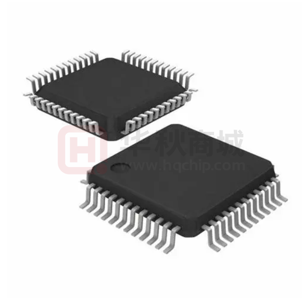
· 44/52/64-pin LQFP packages
HT1622G: Gold bumped chip
· Built-in LCD display RAM
General Description
HT1622 is a peripheral device specially designed for I/O
type MCU used to expand the display capability. The
max. display segment of the device are 256 patterns
(32´8). It also supports serial interface, buzzer sound,
Watchdog Timer or time base timer functions. The
HT1622 is a memory mapping and multi-function LCD
controller. The software configuration feature of the
HT1622 make it suitable for multiple LCD applications including LCD modules and display subsystems. Only
three lines are required for the interface between the host
controller and the HT1622. The HT162X series have
many kinds of products that match various applications.
Selection Table
HT162X
HT1620
HT1621
HT1622
HT16220
HT1623
HT1625
HT1626
COM
4
4
8
8
8
8
16
SEG
32
32
32
32
48
64
48
Built-in Osc.
¾
Ö
Ö
¾
Ö
Ö
Ö
Crystal Osc.
Ö
Ö
¾
Ö
Ö
Ö
Ö
Rev. 2.70
1
November 25, 2014
�PATENTED
HT1622/HT1622G
Block Diagram
D is p la y R A M
O S C I
C S
C o n
a n
T im
C ir c
R D
W R
tro l
d
in g
u it
C O M 0
C O M 7
L C D D r iv e r /
B ia s C ir c u it
D A T A
S E G 0
S E G 3 1
V D D
V L C D
V S S
B Z
T o n e F re q u e n c y
G e n e ra to r
B Z
W a tc h d o g T im e r
a n d
T im e B a s e G e n e r a to r
IR Q
Pin Assignment
S E G
S E G
S E G
S E G
S E G
S E G
S E G
S E G
S E G
S E G
S E G
1 3
1 4
1 5
1 6
1 7
1 8
1 9
2 0
2 1
2 2
2 3
4 4 4 3 4 2 4 1 4 0 3 9 3 8 3 7 3 6 3 5 3 4
1
2
3 3
3
3 1
3
2
S E G
S E G
C O M
C O M
C O M
C O M
C O M
C O M
C O M
C O M
T 3
1
0
7
6
5
4
3
2
1
0
S E G
S E G
S E G
S E G
S E G
S E G
S E G
S E G
S E G
S E G
S E G
S E G
S E G
1 9
2 0
2 1
2 2
2 3
2 4
2 5
2 6
2 7
2 8
2 9
3 0
3 1
5 2 5 1 5 0 4 9 4 8 4 7 4 6 4 5 4 4 4 3 4 2 4 1 4 0
1
3 9
3 8
2
3 7
3
3 6
4
1 0
1 1
1 2
1 3
1 4
1 5
1 6
1 7 1 8 1 9 2 0 2 1 2 2 2 3 2 4 2 5 2 6 2 7 2 8 2 9 3 0 3 1 3 2
5
1 7
1 6
1 5
1 4
1 3
1 2
1 1
1 0
9
8
7
6
5
4
3
4
2
1 4 1 5 1 6 1 7 1 8 1 9 2 0 2 1 2 2 2 3 2 4 2 5 2 6
9
1
1 3
H T 1 6 2 2
6 4 L Q F P -A
1 8
7
1 2
8
0
1 1
7
4 3
4 2
4 1
4 0
3 9
3 8
3 7
3 6
3 5
3 4
3 3
1 9
6
1 0
6
S E G
S E G
S E G
S E G
S E G
S E G
S E G
S E G
S E G
S E G
S E G
S E G
S E G
N C
N C
N C
5
9
4 4
4
8
6
5
4 5
4
3
H T 1 6 2 2
5 2 L Q F P -A
7
3 4
3 3
3 2
3 1
3 0
2 9
2 8
2 7
7
4 6
2
6
8
3
1
3 5
G 1
G 1
G 1
G 1
G 1
G 1
G 1
G 1
G 1
G 9
G 8
G 7
G 6
4 8
4 7
2
0
5
S E
S E
S E
S E
S E
S E
S E
S E
S E
S E
S E
S E
S E
6 4 6 3 6 2 6 1 6 0 5 9 5 8 5 7 5 6 5 5 5 4 5 3 5 2 5 1 5 0 4 9
1
S E G
S E G
S E G
S E G
S E G
S E G
S E G
C O M
C O M
C O M
C O M
C O M
C O M
N C
C O M
C O M
C S
R D
W R
D A T A
V S S
O S C I
V D D
V L C D
IR Q
T 1
T 2
T 3
C O M 0
N
4
N
N
1 2 1 3 1 4 1 5 1 6 1 7 1 8 1 9 2 0 2 1 2 2
2 3
N
1 1
2 4
C S
N C
R D
W R
D A T A
V S S
O S C I
V D D
V L C D
IR Q
B Z
N C
B Z
T 1
T 2
T 3
C
C
C
C
2 0
2 5
1 0
5
2 1
9
6
2 2
2 6
2 3
8
7
2 4
2 7
8
2 5
7
2 8
2 6
6
9
2 7
2 9
H T 1 6 2 2
4 4 L Q F P -A
2 8
5
1 0
2 9
3 0
1 1
3 0
4
1 2
3 1
S E G
S E G
S E G
S E G
S E G
S E G
S E G
S E G
S E G
S E G
S E G
3 2
S E G
S E G
S E G
S E G
S E G
S E G
S E G
S E G
S E G
S E G
S E G
S E G
C S
R D
W R
D A T A
V S S
O S C I
V D D
V L C D
IR Q
T 1
T 2
3
2
1
0
S E G
S E G
S E G
S E G
S E G
S E G
C O M
C O M
C O M
C O M
C O M
C O M
C O M
5
4
3
2
1
0
7
6
5
4
3
2
1
Rev. 2.70
2
November 25, 2014
�PATENTED
HT1622/HT1622G
Pad Assignment
S E G 2 6
S E G 2 5
S E G 2 4
S E G 2 3
S E G 2 2
S E G 2 1
S E G 2 0
5 4
5 3
5 2
5 1 5 0
4 9
4 8
4 7
4 6
4 5
4 4
4 3
3
D A T A
V S
O S
V D
V L C
IR
S E G 2 7
S E G 2 8
2
S E G 2 9
R D
W R
S E G 3 0
1
S E G 3 1
C S
4
5
S
C I
D
D
Q
6
7
8
9
2 1 2 2
2 4
2 5
2 6
2 7 2 8
S E G
S E G
S E G
S E G
S E G
S E G
1 9
S E G
S E G
S E G
S E G
1 3
3 2
3 1
3 0
S E G 9
S E G 8
S E G 7
1 8
1 7
1 6
1 5
1 4
1 2
1 1
1 0
2 9
S E G 5
S E G 6
2 3
S E G 4
S E G 3
2 0
S E G 2
1 9
C O M 6
1 8
C O M 7
1 7
S E G 1
1 2
1 3
1 4
1 5
1 6
S E G 0
T 1
T 2
T 3
C O M 0
C O M 5
1 1
C O M 4
B Z
C O M 3
1 0
C O M 2
B Z
C O M 1
(0 ,0 )
4 2
4 1
4 0
3 9
3 8
3 7
3 6
3 5
3 4
3 3
Chip size: 94 ´ 98 (mil)2
Bump height: 18mm ± 3mm
Min. Bump spacing: 23.102mm
Bump size: 76 ´ 76mm2
* The IC substrate should be connected to VDD in the PCB layout artwork.
Rev. 2.70
3
November 25, 2014
�PATENTED
HT1622/HT1622G
Pad Coordinates
Unit: mm
Pad No.
X
Y
Pad No.
X
Y
1
2
3
4
5
6
7
8
9
10
11
12
13
14
15
16
17
18
19
20
21
22
23
24
25
26
27
-1077.075
-1077.075
-1077.075
-1077.075
-1077.037
-1077.075
-1077.037
-1077.075
-1077.075
-1077.075
-1077.075
-1077.075
-1077.075
-1077.075
-1077.075
-1077.075
-589.281
-490.179
-304.799
-205.699
-20.319
78.736
225.736
324.836
423.856
522.957
621.975
1090.589
905.211
806.109
594.542
359.680
260.745
162.710
63.734
-34.789
-238.247
-519.705
-677.315
-776.416
-875.435
-974.536
-1073.554
-1129.575
-1129.575
-1129.575
-1129.575
-1129.575
-1129.575
-1129.575
-1129.575
-1129.575
-1129.575
-1129.575
28
29
30
31
32
33
34
35
36
37
38
39
40
41
42
43
44
45
46
47
48
49
50
51
52
53
54
721.077
820.095
1076.900
1076.900
1076.900
1076.900
1076.900
1076.900
1076.900
1076.900
1076.900
1076.900
1076.900
1076.900
1076.900
213.669
114.650
15.550
-83.469
-182.570
-281.590
-380.690
-479.710
-578.810
-677.829
-776.931
-875.949
-1129.575
-1129.575
-141.904
-42.885
56.215
155.234
254.335
353.354
452.456
551.474
650.576
749.594
848.695
947.714
1046.816
1127.150
1127.150
1127.150
1127.150
1127.150
1127.150
1127.150
1127.150
1127.150
1127.150
1127.150
1127.150
Pad Description
Pad No.
1
Pad Name
CS
I/O
Description
I
Chip selection input with Pull-high resistor. When the CS is logic high, the
data and command read from or written to the HT1622 are disabled. The serial interface circuit is also reset. But if CS is at logic low level and is input to
the CS pad, the data and command transmission between the host controller
and the HT1622 are all enabled.
2
RD
I
READ clock input with Pull-high resistor. Data in the RAM of the HT1622 are
clocked out on the falling edge of the RD signal. The clocked out data will appear on the data line. The host controller can use the next rising edge to latch
the clocked out data.
3
WR
I
WRITE clock input with Pull-high resistor. Data on the DATA line are latched
into the HT1622 on the rising edge of the WR signal.
4
DATA
I/O
Serial data input or output with Pull-high resistor
5
VSS
¾
Negative power supply, ground
6
OSCI
I
7
VDD
¾
8
VLCD
I
LCD operating voltage input pad
If the system clock comes from an external clock source, the external clock
source should be connected to the OSCI pad.
Positive power supply
9
IRQ
O
Time base or Watchdog Timer overflow flag, NMOS open drain output
10, 11
BZ, BZ
O
2kHz or 4kHz tone frequency output pair
12~14
T1~T3
I
Not connected
15~22
COM0~COM7
O
LCD common outputs
23~54
SEG0~SEG31
O
LCD segment outputs
Rev. 2.70
4
November 25, 2014
�PATENTED
HT1622/HT1622G
Absolute Maximum Ratings
Supply Voltage ...........................VSS-0.3V to VSS+5.5V
Storage Temperature ............................-50°C to 125°C
Input Voltage.............................VSS-0.3V to VDD+0.3V
Operating Temperature...........................-40°C to 85°C
Note: These are stress ratings only. Stresses exceeding the range specified under ²Absolute Maximum Ratings² may
cause substantial damage to the device. Functional operation of this device at other conditions beyond those listed
in the specification is not implied and prolonged exposure to extreme conditions may affect device reliability.
D.C. Characteristics
Symbol
Parameter
VDD
Operating Voltage
IDD1
Operating Current
Ta=25°C
Test Conditions
VDD
Conditions
¾
¾
3V
5V
IDD2
3V
Operating Current
5V
ISTB
No load/LCD ON
On-chip RC oscillator
No load/LCD OFF
On-chip RC oscillator
3V
Standby Current
No load, Power Down Mode
5V
VIL
3V
Input Low Voltage
3V
Input High Voltage
IOH1
IOL2
IOH2
IOL3
IOH3
IOL4
IOH4
RPH
Unit
2.7
¾
5.2
V
¾
80
210
mA
¾
135
415
mA
¾
8
30
mA
¾
20
55
mA
¾
1
8
mA
¾
2
16
mA
0
¾
0.6
V
0
¾
1.0
V
2.4
¾
3.0
V
4.0
¾
5.0
V
3V
VOL=0.3V
0.9
1.8
¾
mA
5V
VOL=0.5V
1.7
3.0
¾
mA
3V
VOH=2.7V
-0.9
-1.8
¾
mA
5V
VOH=4.5V
-1.7
-3.0
¾
mA
3V
VOL=0.3V
200
450
¾
mA
5V
VOL=0.5V
250
500
¾
mA
3V
VOH=2.7V
-200
-450
¾
mA
5V
VOH=4.5V
-250
-500
¾
mA
3V
VOL=0.3V
15
40
¾
mA
5V
VOL=0.5V
100
200
¾
mA
3V
VOH=2.7V
-15
-30
¾
mA
5V
VOH=4.5V
-45
-90
¾
mA
3V
VOL=0.3V
15
30
¾
mA
5V
VOL=0.5V
70
150
¾
mA
3V
VOH=2.7V
-6
-13
¾
mA
5V
VOH=4.5V
-20
-40
¾
mA
100
200
300
kW
50
100
150
kW
BZ, BZ, IRQ
BZ, BZ
DATA
DATA
LCD Common Sink Current
LCD Common Source Current
LCD Segment Sink Current
LCD Segment Source Current
3V
Pull-high Resistor
DATA, WR, CS, RD
5V
Rev. 2.70
Max.
DATA, WR, CS, RD
5V
IOL1
Typ.
DATA, WR, CS, RD
5V
VIH
Min.
5
November 25, 2014
�PATENTED
HT1622/HT1622G
A.C. Characteristics
Symbol
Parameter
Ta=25°C
Test Conditions
Min.
Typ.
Max.
Unit
On-chip RC oscillator
24
32
40
kHz
External clock source
¾
32768
¾
Hz
On-chip RC oscillator
48
64
80
Hz
¾
External clock source
¾
64
¾
Hz
¾
n: Number of COM
¾
n/fLCD
¾
sec
4
¾
150
kHz
4
¾
300
kHz
¾
¾
75
kHz
¾
¾
150
kHz
CS
500
600
¾
ns
Write mode
3.34
¾
125
Read mode
6.67
¾
¾
Write mode
1.67
¾
125
Read mode
3.34
¾
¾
VDD
Conditions
3V
fSYS
System Clock
5V
¾
3V
fLCD
LCD Frame Frequency
tCOM
LCD Common Period
fCLK1
Serial Data Clock (WR pin)
5V
3V
Duty cycle 50%
5V
3V
fCLK2
Serial Data Clock (RD pin)
Duty cycle 50%
5V
Serial Interface Reset Pulse Width
(Figure 3)
tCS
¾
3V
tCLK
WR, RD Input Pulse Width (Figure 1)
5V
ms
ms
t r, t f
Rise/Fall Time Serial Data Clock Width
(Figure 1)
¾
¾
¾
120
160
ns
tsu
Setup Time for DATA to WR, RD Clock
Width (Figure 2)
¾
¾
60
120
¾
ns
th
Hold Time for DATA to WR, RD, Clock
Width (Figure 2)
¾
¾
500
600
¾
ns
tsu1
Setup Time for CS to WR, RD Clock
Width (Figure 3)
¾
¾
500
600
¾
ns
th1
Hold Time for CS to WR, RD Clock
Width (Figure 3)
¾
¾
700
800
¾
ns
On-chip RC oscillator
1.5
2.0
2.5
kHz
On-chip RC oscillator
3
4
5
kHz
20
¾
¾
ms
0.05
¾
¾
V/ms
1
¾
¾
ms
3V
Tone Frequency (2kHz)
5V
fTONE
3V
Tone Frequency (4kHz)
5V
tOFF
VDD OFF Times (Figure 4)
¾
VDD drop down to 0V
tSR
VDD Rising Slew Rate (Figure 4)
¾
¾
tRSTD
Delay Time after Reset (Figure 4)
¾
Note:
¾
1. If the conditions of Power-on Reset timing are not satisfied in power On/Off sequence, the internal
Power-on Reset (POR) circuit will not operate normally.
2. If the VDD drops below the minimum voltage of operating voltage spec. during operating, the conditions
of Power-on Reset timing must be satisfied also. That is, the VDD must drop to 0V and keep at 0V for
20ms (min.) before rising to the normal operating voltage.
Rev. 2.70
6
November 25, 2014
�PATENTED
HT1622/HT1622G
V A L ID D A T A
D B
tf
W R , R D
C lo c k
9 0 %
5 0 %
1 0 %
tr
tC
V
tC
L K
G N D
W R , R D
C lo c k
W R , R D
C lo c k
V D D
S
V
th
G N D
0 V
1
V
5 0 %
F ir s t C lo c k
tS
D D
5 0 %
u 1
D D
G N D
Figure 2
tC
ts
V
5 0 %
Figure 1
C S
D D
G N D
th
tsu
D D
L K
V
5 0 %
tO
R
F F
D D
0 .9 V
D D
tR
S T D
G N D
L a s t C lo c k
C S
Figure 3
Figure 4. Power-on Reset Timing
RC Oscillator Frequency Deviation
Operating Temperature
-40°C
0°C
25°C
70°C
75°C
80°C
85°C
Average Deviation
19.85%
2.98%
0
-21.14%
-22.50%
-23.82%
-25.35%
Rev. 2.70
7
November 25, 2014
�PATENTED
HT1622/HT1622G
Functional Description
Display Memory - RAM Structure
remain at logic low level until the CLR WDT or the IRQ
DIS command is issued.
The static display RAM is organized into 64´4 bits and
stores the display data. The contents of the RAM are directly mapped to the contents of the LCD driver. Data in
the RAM can be accessed by the READ, WRITE and
READ-MODIFY-WRITE commands. The following is a
mapping from the RAM to the LCD patterns.
If an external clock is selected as the source of system
frequency, the SYS DIS command turns out invalid and
the power down mode fails to be carried out until the external clock source is removed.
Buzzer Tone Output
Time Base and Watchdog Timer (WDT)
A simple tone generator is implemented in the HT1622.
The tone generator can output a pair of differential driving signals on the BZ and BZ which are used to generate
a single tone.
The time base generator and WDT share the same divided (¸256) counter. TIMER DIS/EN/CLR, WDT
DIS/EN/CLR and IRQ EN/DIS are independent from each
other. Once the WDT time-out occurs, the IRQ pin will
C O M 7
C O M 6
C O M 5
C O M 3
C O M 4
C O M 2
C O M 1
C O M 0
S E G 0
1
0
S E G 1
3
2
S E G 2
5
4
S E G 3
7
6
S E G 3 1
6 3
6 2
D 3
D 2
D 1
D 0
A d d r
D a ta
D 3
D 2
D 1
D 0
A d d r e s s 6 B its
(A 5 , A 4 , ...., A 0 )
A d d r
D a ta
D a ta 4 B its
(D 3 , D 2 , D 1 , D 0 )
RAM Mapping
T im e B a s e
C lo c k S o u r c e
T IM E R
¸ 2 5 6
V
C L R T im e r
W D T
¸ 4
D D
Q
D
C K
C L R
IR Q
E N /D IS
W D T E N /D IS
IR Q
E N /D IS
R
W D T
Timer and WDT Configurations
Rev. 2.70
8
November 25, 2014
�PATENTED
Command Format
If successive commands have been issued, the command mode ID can be omitted. While the system is ope r a t i n g i n a n o n - su cce ssi ve co m m a n d o r a
non-successive address data mode, the CS pin should
be set to ²1² and the previous operation mode will be reset also. The CS pin returns to ²0², a new operation
mode ID should be issued first.
The HT1622 can be configured by the software setting.
There are two mode commands to configure the
HT1622 resource and to transfer the LCD display data.
The following are the data mode ID and the command
mode ID:
Mode
ID
READ
Operation
Data
110
WRITE
Data
101
READ-MODIFY-WRITE
COMMAND
Name
Data
101
Command
100
HT1622/HT1622G
Command Code
Function
TONE OFF
0000-1000-X
Turn-off tone output
TONE 4K
010X-XXXX-X
Turn-on tone output, tone frequency is 4kHz
TONE 2K
0110-XXXX-X
Turn-on tone output, tone frequency is 2kHz
Timing Diagrams
READ Mode (Command Code : 1 1 0)
C S
W R
R D
D A T A
1
0
1
A 5 A 4 A 3 A 2 A 1 A 0 D 0 D 1 D 2 D 3
M e m o ry A d d re s s 1 (M A 1 ) D a ta (M A 1 )
1
1
0
A 5 A 4 A 3 A 2 A 1 A 0 D 0 D 1 D 2 D 3
M e m o r y A d d r e s s 2 ( M A 2 )D a t a ( M A 2 )
READ Mode (Successive Address Reading)
C S
W R
R D
D A T A
Rev. 2.70
1
1
0
A 5 A 4 A 3 A 2 A 1 A 0 D 0 D 1 D 2 D 3 D 0 D 1 D 2 D 3 D 0 D 1 D 2 D 3 D 0 D 1 D 2 D 3 D 0
D a ta (M A + 1 ) D a ta (M A + 2 ) D a ta (M A + 3 )
M e m o ry A d d re s s (M A ) D a ta (M A )
9
November 25, 2014
�PATENTED
HT1622/HT1622G
WRITE Mode (Command Code : 1 0 1)
C S
W R
1
D A T A
1
0
A 5 A 4 A 3 A 2 A 1 A 0 D 0 D 1 D 2 D 3
M e m o r y A d d r e s s 1 ( M A 1 )D a t a ( M A 1 )
1
1
0
A 5 A 4 A 3 A 2 A 1 A 0 D 0 D 1 D 2 D 3
M e m o r y A d d r e s s 2 ( M A 2 )D a t a ( M A 2 )
WRITE Mode (Successive Address Writing)
C S
W R
1
D A T A
1
0
A 5 A 4 A 3 A 2 A 1 A 0 D 0 D 1 D 2 D 3 D 0 D 1 D 2 D 3 D 0 D 1 D 2 D 3 D 0 D 1 D 2 D 3 D 0
D a ta (M A + 1 ) D a ta (M A + 2 ) D a ta (M A + 3 )
M e m o ry A d d re s s (M A ) D a ta (M A )
READ-MODIFY-WRITE Mode (Command Code : 1 0 1)
C S
W R
R D
D A T A
1
1
0
A 5 A 4 A 3 A 2 A 1 A 0 D 0 D 1 D 2 D 3 D 0 D 1 D 2 D 3
M e m o r y A d d r e s s 1 ( M A 1 )D a t a ( M A 1 )
D a ta (M A 1 )
1
0
1
A 5 A 4 A 3 A 2 A 1 A 0 D 0 D 1 D 2 D 3
M e m o r y A d d r e s s 2 ( M A 2 )D a t a ( M A 2 )
READ-MODIFY-WRITE Mode (Successive Address Accessing)
C S
W R
R D
D A T A
Rev. 2.70
1
0
1
A 5 A 4 A 3 A 2 A 1 A 0 D 0 D 1 D 2 D 3 D 0 D 1 D 2 D 3 D 0 D 1 D 2 D 3 D 0 D 1 D 2 D 3 D 0 D 1 D 2 D 3 D 0
D a ta (M A )
D a ta (M A + 1 ) D a ta (M A + 1 ) D a ta (M A + 2 )
M e m o ry A d d re s s (M A ) D a ta (M A )
10
November 25, 2014
�PATENTED
HT1622/HT1622G
Command Mode (Command Code : 1 0 0)
C S
W R
D A T A
1
0
0
C 8 C 7 C 6 C 5 C 4 C 3 C 2 C 1 C 0
C 8 C 7 C 6 C 5 C 4 C 3 C 2 C 1 C 0
C o m m a n d 1
C o m m a n d ...
C o m m a n d i
C o m m a n d
o r
D a ta M o d e
Mode (Data and Command Mode)
C S
W R
D A T A
C o m m a n d
o r
D a ta M o d e
A d d re s s a n d D a ta
C o m m a n d
o r
D a ta M o d e
A d d re s s a n d D a ta
C o m m a n d
o r
D a ta M o d e
A d d re s s a n d D a ta
R D
Rev. 2.70
11
November 25, 2014
�PATENTED
HT1622/HT1622G
Application Circuits
C S
*
V D D
R D
H T 1 6 2 2
D A T A
*
V R
V L C D
W R
M C U
*
B Z
P ie z o
R
IR Q
B Z
C O M 0 ~ C O M 7
S E G 0 ~ S E G 3 1
1 /4 B ia s , 1 /8 D u ty
L C D
Note:
P a n e l
The connection of IRQ and RD pin can be selected depending on the requirement of the MCU.
The voltage applied to VLCD pin must be equal to or lower than VDD.
Adjust VR to fit user's LCD panel display voltage (VLCD).
Adjust R (external pull-high resistance) to fit user¢s time base clock.
Command Summary
Name
ID
Command Code
D/C
Function
Def.
READ
1 1 0 A5A4A3A2A1A0D0D1D2D3
D
Read data from the RAM
WRITE
1 0 1 A5A4A3A2A1A0D0D1D2D3
D
Write data to the RAM
READ-MODIFYWRITE
1 0 1 A5A4A3A2A1A0D0D1D2D3
D
Read and Write data to the RAM
SYS DIS
1 0 0 0000-0000-X
C
Turn off both system oscillator and LCD bias
Yes
generator
SYS EN
1 0 0 0000-0001-X
C
Turn on system oscillator
LCD OFF
1 0 0 0000-0010-X
C
Turn off LCD display
LCD ON
1 0 0 0000-0011-X
C
Turn on LCD display
TIMER DIS
1 0 0 0000-0100-X
C
Disable time base output
Yes
WDT DIS
1 0 0 0000-0101-X
C
Disable WDT time-out flag output
Yes
TIMER EN
1 0 0 0000-0110-X
C
Enable time base output
WDT EN
1 0 0 0000-0111-X
C
Enable WDT time-out flag output
TONE OFF
1 0 0 0000-1000-X
C
Turn off tone outputs
CLR TIMER
1 0 0 0000-1101-X
C
Clear the contents of the time base generator
CLR WDT
1 0 0 0000-1111-X
C
Clear the contents of WDT stage
RC 32K
1 0 0 0001-10XX-X
C
System clock source, on-chip RC oscillator
EXT 32K
1 0 0 0001-11XX-X
C
System clock source, external clock source
TONE 4K
1 0 0 010X-XXXX-X
C
Tone frequency output: 4kHz
TONE 2K
1 0 0 0110-XXXX-X
C
Tone frequency output: 2kHz
IRQ DIS
1 0 0 100X-0XXX-X
C
Disable IRQ output
IRQ EN
1 0 0 100X-1XXX-X
C
Enable IRQ output
Rev. 2.70
12
Yes
Yes
Yes
Yes
November 25, 2014
�PATENTED
Name
ID
Command Code
D/C
HT1622/HT1622G
Function
Def.
F1
1 0 0 101X-0000-X
C
Time base clock output: 1Hz
The WDT time-out flag after: 4s
F2
1 0 0 101X-0001-X
C
Time base clock output: 2Hz
The WDT time-out flag after: 2s
F4
1 0 0 101X-0010-X
C
Time base clock output: 4Hz
The WDT time-out flag after: 1s
F8
1 0 0 101X-0011-X
C
Time base clock output: 8Hz
The WDT time-out flag after: 1/2s
F16
1 0 0 101X-0100-X
C
Time base clock output: 16Hz
The WDT time-out flag after: 1/4s
F32
1 0 0 101X-0101-X
C
Time base clock output: 32Hz
The WDT time-out flag after: 1/8s
F64
1 0 0 101X-0110-X
C
Time base clock output: 64Hz
The WDT time-out flag after: 1/16s
F128
1 0 0 101X-0111-X
C
Time base clock output: 128Hz
The WDT time-out flag after: 1/32s
TEST
1 0 0 1110-0000-X
C
Test mode, user don¢t use.
NORMAL
1 0 0 1110-0011-X
C
Normal mode
Note:
Yes
Yes
X : Don¢t care
A5~A0 : RAM address
D3~D0 : RAM data
D/C : Data/Command mode
Def. : Power on reset default
All the bold forms, namely 1 1 0, 1 0 1, and 1 0 0, are mode commands. Of these, 1 0 0 indicates the command
mode ID. If successive commands have been issued, the command mode ID except for the first command will
be omitted. The source of the tone frequency and of the time base or WDT clock frequency can be derived from
an on-chip 32kHz RC oscillator or an external 32768Hz clock. Calculation of the frequency is based on the system frequency sources as stated above. It is recommended that the host controller should initialize the HT1622
after power on reset, for power on reset may fail, which in turn leads to the malfunctioning of the HT1622.
Rev. 2.70
13
November 25, 2014
�PATENTED
HT1622/HT1622G
Package Information
Note that the package information provided here is for consultation purposes only. As this information may be updated
at regular intervals users are reminded to consult the Holtek website for the latest version of the package information.
Additional supplementary information with regard to packaging is listed below. Click on the relevant section to be transferred to the relevant website page.
· Further Package Information (include Outline Dimensions, Product Tape and Reel Specifications)
· Packing Meterials Information
· Carton information
Rev. 2.70
14
November 25, 2014
�PATENTED
HT1622/HT1622G
44-pin LQFP (10mm´10mm) (FP2.0mm) Outline Dimensions
H
C
D
G
2 3
3 3
I
3 4
2 2
F
A
B
E
1 2
4 4
K
a
J
1
Symbol
A
Dimensions in inch
Min.
Nom.
Max.
¾
0.472 BSC
¾
B
¾
0.394 BSC
¾
C
¾
0.472 BSC
¾
D
¾
0.394 BSC
¾
E
¾
0.032 BSC
¾
F
0.012
0.015
0.018
G
0.053
0.055
0.057
H
¾
¾
0.063
I
0.002
¾
0.006
J
0.018
0.024
0.030
K
0.004
¾
0.008
a
0°
¾
7°
Symbol
Rev. 2.70
1 1
Dimensions in mm
Min.
Nom.
Max.
A
¾
12.00 BSC
¾
B
¾
10.00 BSC
¾
C
¾
12.00 BSC
¾
D
¾
10.00 BSC
¾
E
¾
0.80 BSC
¾
F
0.30
0.37
0.45
G
1.35
1.40
1.45
H
¾
¾
1.60
I
0.05
¾
0.15
J
0.45
0.60
0.75
K
0.09
¾
0.20
a
0°
¾
7°
15
November 25, 2014
�PATENTED
HT1622/HT1622G
52-pin LQFP (14mm´14mm) Outline Dimensions
C
H
D
3 9
G
2 7
I
2 6
4 0
F
A
B
E
1 4
5 2
K
J
1
Symbol
A
Dimensions in inch
Min.
Nom.
Max.
0.622
0.630
0.638
B
0.547
0.551
0.555
C
0.622
0.630
0.638
D
0.547
0.551
0.555
E
¾
0.039 BSC
¾
F
0.015
¾
0.019
G
0.053
0.055
0.057
H
¾
¾
0.063
I
0.002
¾
0.008
J
0.018
¾
0.030
K
0.005
¾
0.007
a
0°
¾
7°
Symbol
A
Rev. 2.70
1 3
Dimensions in mm
Min.
Nom.
Max.
15.80
16.00
16.20
B
13.90
14.00
14.10
C
15.80
16.00
16.20
D
13.90
14.00
14.10
E
¾
1.0 BSC
¾
F
0.39
¾
0.48
G
1.35
1.40
1.45
H
¾
¾
1.60
I
0.05
¾
0.20
J
0.45
¾
0.75
K
0.13
¾
0.18
a
0°
¾
7°
16
November 25, 2014
�PATENTED
HT1622/HT1622G
64-pin LQFP (7mm´7mm) Outline Dimensions
C
D
4 8
G
3 3
H
I
3 2
4 9
F
A
B
E
6 4
1 7
K
a
J
1 6
1
Symbol
Nom.
Max.
A
¾
0.354 BSC
¾
B
¾
0.276 BSC
¾
C
¾
0.354 BSC
¾
D
¾
0.276 BSC
¾
E
¾
0.020 BSC
¾
F
0.005
0.007
0.009
G
0.053
0.055
0.057
H
¾
¾
0.063
I
0.002
¾
0.006
J
0.018
0.024
0.030
K
0.004
¾
0.008
a
0°
¾
7°
Symbol
Rev. 2.70
Dimensions in inch
Min.
Dimensions in mm
Min.
Nom.
Max.
A
¾
9.00 BSC
¾
B
¾
7.00 BSC
¾
C
¾
9.00 BSC
¾
D
¾
7.00 BSC
¾
E
¾
0.40 BSC
¾
F
0.13
0.18
0.23
G
1.35
1.40
1.45
H
¾
¾
1.60
I
0.05
¾
0.15
J
0.45
0.60
0.75
K
0.09
¾
0.20
a
0°
¾
7°
17
November 25, 2014
�PATENTED
HT1622/HT1622G
Copyright Ó 2014 by HOLTEK SEMICONDUCTOR INC.
The information appearing in this Data Sheet is believed to be accurate at the time of publication. However, Holtek assumes no responsibility arising from the use of the specifications described. The applications mentioned herein are used solely for the purpose of illustration and
Holtek makes no warranty or representation that such applications will be suitable without further modification, nor recommends the use of its products for application that may present a
risk to human life due to malfunction or otherwise. Holtek¢s products are not authorized for use
as critical components in life support devices or systems. Holtek reserves the right to alter its
products without prior notification. For the most up-to-date information, please visit our web
site at http://www.holtek.com.tw.
Rev. 2.70
18
November 25, 2014
�