High Temperature Analog Multiplexers
16-Channel Single-Ended / 8-Channel Differential
HT506 / HT507
The High Temperature HT506/HT507 monolithic multiplexers consist of sixteen analog switches, 4-bit decode for channel
selection, reference for logic switching thresholds, and enable pin for device deactivation where applications require.
These multiplexers are fabricated with Honeywell’s dielectrically isolated latch-up free high temperature (HTMOS™) linear
process. Performance is specified over the full -55 to +225ºC temperature range. Typically, parts will operate up to
+300ºC for a year, with derated performance. All parts are burned in at 250ºC. The input buffers are designed to operate
from either TTL or CMOS levels while providing a break-before-make action. The HT506 switches one of the sixteen
single-ended inputs to a common output, while the HT507 switches one of the eight differential inputs to a differential
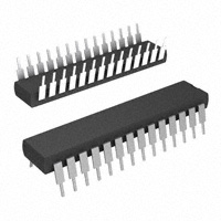
output. These parts are available in standard pinout 28-pin DIP Ceramic Packages.
Applications
Down-Hole Oil, Gas, and Geothermal Well
Avionics
Turbine Engine Control
Industrial Process Control
Electric Power Conversion
Heavy Duty Internal Combustion Engine
FEATURES AND BENEFITS
Specified over -55 to +225 C
Designed to continuously operate for at
least 5 years at 225 C
16:1 Single-Ended or 8:1 Differential
Configuration
Enable and address inputs compatible with TTL
and/or 5V CMOS logic
No latch-up
10V analog input/output range (±5V or 0 to 10V)
On resistance 400Ω at 225ºC
Split and single supply capability
Output leakage less than 2.5µA at 225ºC
Break-Before-Make Switching
�HT506/HT507
PACKAGE PINOUTS
ELECTRICAL CHARACTERISTICS (Split Supply)
Temperature range -55 to +225 C, typical @ +25 C, V+ = +5V, V- = -5V, GND=0V, VIL=0.8, VIH = 2.4V, unless otherwise specified
Symbol
Parameters
Test Conditions
Typical
(1)
Analog Switch
VANALOG
Analog Signal Range
rDS(ON)
Drain-Source On-Resistance
∆rDS(ON)
rDS(ON) Matching between Channels
IS(OFF)
Source Off Leakage Current
ID(OFF)
Drain Off Leakage Current
ID(ON)
Drain On Leakage Current
Digital Control
VIH
Logic High Input Voltage
VIL
Logic Low Input Voltage
IIH
Logic High Input Current
IIL
Logic Low Input Current
CIN
Logic Input Capacitance
Dynamic Characteristics
tON
Address/Enable Turn-On Time
tOFF
Address/Enable Turn-Off Time
Q
Charge Injection
OIS
Off Isolation
Power Supplies
I+
Positive Supply Current
INegative Supply Current
Worst Case
(2)
MIN
MAX
-5
VD ±5V, IS = -10mA Sequence
Each Switch On
VD = ±5V
VEN = 0V
VD= ±5V, VEN = 0V, VS = ±5V
Sequence Each Switch On
5
V
100
400
Ω
2
0.01
0.04
0.04
200
2500
2500
%
nA
nA
nA
-2500
-2500
2.4
0.8
VA = 2.4V, 10V
VEN = 0V, 2.4V, VA =0V
f=1MHz
trise/tfall
很抱歉,暂时无法提供与“HT506”相匹配的价格&库存,您可以联系我们找货
免费人工找货