HTMOSTM High Temperature Products
Advanced Information
HIGH TEMPERATURE N-CHANNEL POWER FET
HTNFET
FEATURES
APPLICATIONS
• Specified Over -55 to +225°C
• Down-Hole Oil, Gas and Geothermal Well
• Output Current up to 1 Amp Continuous
• Aerospace and Avionics
• Typical Input Voltage up to 60V
• Turbine Engine Control
• Silicon-On-Insulator (SOI)
• Industrial Process Control
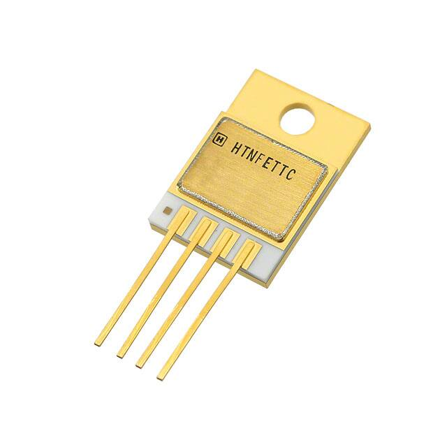
• 4-Pin Power-Tab Package,
• Nuclear Reactor
8-Pin Ceramic Dip with Integral Heat Sink or
• Electric Power Conversion
Die Dimensions 4.699 x 2.286 mm
• Heavy Duty Internal Combustion Engines
GENERAL DESCRIPTION
The HTNFET is a high reliability N-Channel Power FET
designed specifically for extremely wide temperature
range applications such as down-hole instrumentation,
aerospace, turbine engine and industrial process control.
This power FET is fabricated using a Silicon-On-Insulator
(SOI) process that dramatically reduces leakage currents
at high temperatures.
High DC current capability combined with low Rds-ON make
this component suitable both for DC and switching applications. Typically, parts will operate at +300°C up to a year,
with derated performance. All parts are burned in to eliminate infant mortality. Additionally, each part is tested over 55 to +225°C to provide guaranteed performance over the
entire temperature band.
FUNCTIONAL DIAGRAM
PACKAGE DIAGRAMS
Drain
8-Pin Ceramic DIP With Heat Sink
4-Pin Power-Tab Package
Gate
Source
Drain 1
8 Source
Drain 2
7 Gate
Gate 3
6 Source
Drain 4
5 Source
DIE DIAGRAM
Solid State Electronics Center • 12001 State Highway 55, Plymouth, MN 55441 • (800) 323-8295 • http://www.ssec.honeywell.com
�HTNFET
ELECTRICAL CHARACTERISTICS
Symbol
-55 to +225°C, unless otherwise specified
Parameters
Test Conditions
Typ (1)
Worst Case (2)
Min
V(BR)DSS Drain-source breakdown voltage
55
VGS = 0, ID = 100 μADC
RDS (on)
Static drain-to-source on-state
resistance @ Ta=25° C
VGS = +5VDC, ID = 0.1A
0.4
VGS (th)
Gate threshold voltage @
Ta=25° C
VGS = VDS, ID = 100 μA
1.6
IGSS
Units
Max
V
Ω
2.4
V
Gate-to-source forward leakage
VGS = +5 VDC
100
nA
Gate-to-source reverse leakage
VGS = -5 VDC
-100
nA
Guaranteed by design
Qg
Total gate charge (CGS + CGD)
td (on)
Turn-on delay time
tr
Rise time
td (off)
Turn-off delay time
tf
Fall time
Ciss
Input capacitance
VDD = +50 V; VGS = +5 V (VGS, sweep
= 0 to +10 V); d = 10%; τ = 1 ms
4.3
nC
VDD=+50 V;
10
ns
VGS, sweep = 0 to +10 V;
20
ns
d= 0.1%; τ= 1 ms;
64
ns
RD= 15 Ω, RG= 30 Ω
20
ns
290
pF
87
pF
14
pF
VGS=0, VDS = +28 V
f = 1.0 MHz (0.1 V oscillation)
Coss
Output capacitance
Crss
Reverse transfer capacitance
(1) Typical operating conditions: VDS = 10 V, TA=25°C.
(2) Worst case operating conditions: VDS = 50 V, TA = -55 to 225°C.
IDSS vs TEMPERATURE
ABSOLUTE MAXIMUM RATINGS (1, 2)
0
50
100
150
200
250
1.00E-04
Conditions
Value
Units
ID
Continuous Drain Current
@Tj = 25° C
TBD
A
ID
Continuous Drain Current
@Tj = 200° C
TBD
A
VGS
Gate-To-Source Voltage
10
V
dv/dt
Peak Diode Recovery
TBD
V/ns
TJ
Operating Junction
-55 to +300
°C
Tstg
Storage Temperature Range
-55 to +300
°C
Pd
Operating Power
50
W (3)
@Tj = 250° C
1.00E-05
1.00E-06
IDSS (A)
Symbol Parameters
1.00E-07
1.00E-08
1.00E-09
1.00E-10
1.00E-11
(1) Stresses in excess of those listed above may result in permanent damage.
These are stress ratings only, and operation at these levels is not implied.
Frequent or extended exposure to absolute maximum conditions may
affect device reliability.
(2) ESD sensitivity is determined by the gate capacitance; additional ESD
protection would decrease performance.
(3) Derate power at 1W/C to Tj = 300°C.
Temperature (C)
VDS = 90 V
VDS = 50 V
VDS = 10 V
Honeywell reserves the right to make changes to any products or technology herein to improve reliability, function or design. Honeywell does not assume any liability
arising out of the application or use of any product or circuit described herein; neither does it convey any license under its patent rights nor the rights of others.
900214 Rev. D
6-04
�
很抱歉,暂时无法提供与“HTNFET-T”相匹配的价格&库存,您可以联系我们找货
免费人工找货