物料型号:
- Agilent ABA-31563
器件简介:
- Agilent的ABA-31563是一款经济实惠、易于使用的内部50欧姆匹配的硅单片宽带放大器,提供从直流到3.5 GHz的优秀增益和宽带响应。采用超小型SOT-363封装,占用的板空间仅为SOT-143封装的一半。
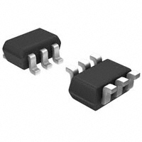
引脚分配:
- 该数据手册提供了顶视图和封装标记,用于方向和识别。
参数特性:
- 工作频率:直流至3.5GHz
- 增益:21.5dB
- 电压驻波比(VSWR):全工作频率下小于2.0
- 输出1dB压缩点功率:2.2dBm
- 输出三阶截取点:13.1dBm
- 噪声系数:3.8dB
- 工作电压:单3V供电(工作电流14~16mA)
- 无铅
功能详解:
- ABA-31563适用于作为移动通信、直播卫星调谐器、LNB以及其他无线通信系统中的低成本增益模块。
- 该器件采用Agilent的HP25硅双极工艺制造,具备高fT和高NPN击穿能力(6V BVCEO下25GHz fT)。
- 该工艺使用行业标准器件氧化隔离技术和亚微米铝多层互连技术,以实现卓越的性能、高均匀性和可靠性。
应用信息:
- 用于移动通信、无线、特殊移动无线电、个人通信服务、工业、科学和医疗、无线局域网、直播卫星、电视接收机和电视调谐器应用的放大器。
封装信息:
- 封装类型:SOT-363/SC70
- 提供了详细的封装尺寸图和PCB布局推荐。