Agilent AMMP-6530 5– 30 GHz Image Reject Mixer
Data Sheet
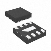
Features • 5x5 mm Surface Mount Package • Broad Band Performance 5 – 30 GHz • Low Conversion Loss of 8 dB • High Image Rejection of 15 – 20 dB • Good 3rd Order Intercept of +18 dBm Description Agilent’s AMMP-6530 is an image reject mixer that operates from 5 GHz to 30 GHz. The cold channel FET mixer is designed to be an easy-to-use component for any surface mount PCB application. It can be used drain pumped for low conversion loss applications, or when gate pumped the mixer can provide high linearity for SSB up-conversion. An external 90-degree hybrid is used to achieve image rejection and a -1V voltage reference is needed. Intended applications include microwave radios, 802.16, VSAT, and satellite receivers. Since this one mixer can cover several bands, the AMMP-6530 can reduce part inventory. The integrated mixer eliminates complex tuning and assembly processes typically required by hybrid (discrete-FET or diode) mixers. The package is fully SMT compatible with backside grounding and I/O to simplify assembly.
8 RF NC 7 Vg 6 NC 5 IF2 3 NC 2 IF1 1
• Single -1V, no current Supply Bias Applications • Microwave Radio Systems • Satellite VSAT, DBS Up/Down Link • LMDS & Pt-Pt mmW Long Haul • Broadband Wireless Access (including 802.16 and 802.20 WiMax) • WLL and MMDS loops • Commercial grade military
gate 4
Pin
1 2 3 4 5 6 7 8
Function
IF1 IF2 LO Vg RF
Top view package base: GND
Absolute Maximum Ratings [1]
Symbol
Vg Pin Tch Tstg Tmax
Parameters/Conditions
Gate Supply Voltage CW Input Power Operating Channel Temperature Storage Case Temperature Max. Assembly Temp (60 sec max)
Units
V dBm °C °C °C
Min.
0
Max.
-3 15 +150
-65
+150 +300
Note: 1. Operation in excess of any one of these conditions may result in permanent damage to this device.
Attention: Observe precautions for handling electrostatic sensitive devices. ESD Machine Model (Class A) ESD Human Body Model (Class 0) Refer to Agilent Application Note A004R: Electrostatic Discharge Damage and Control.
�AMMP-6530 DC Specifications/Physical Properties[1]
Symbol
Ig Vg
Parameters and Test Conditions
Gate Supply Current (under any RF power drive and temperature) Gate Supply Operating Voltage
Units
mA V
Typ.
0 -1V
Note: 1. Ambient operational temperature TA=25°C unless otherwise noted.
AMMP-6530 Typical Performance [2, 3] (TA = 25°C, Vg= -1V, IF frequency = 1 GHz, Zo=50 Ω) Symbol
FRF FLO FIF
Parameters and Test Conditions
RF Frequency Range LO Frequency Range IF Frequency Range
Units
GHz GHz GHz
Gate Pumped
5 – 30 5 – 30 DC – 5
Drain Pumped
5 – 30 5 – 30 DC – 5
Down Conversion
PLO CG RL_RF RL_LO RL_IF IR LO-RF Iso. LO-IF Iso. RF-IF Iso. IIP3 P-1 NF LO Port Pumping Power RF to IF Conversion Gain RF Port Return Loss LO Port Return Loss IF Port Return Loss Image Rejection Ratio LO to RF Port Isolation LO to IF Port Isolation RF to IF Port Isolation Input IP3, Fdelta=100 MHz, Prf = -10 dBm, Plo = 15 dBm Input Port Power at 1dB gain compression point, Plo=+10 dBm Noise Figure dBm dB dB dB dB dB dB dB dB dBm dBm dB >10 -10 5 10 10 15 22 25 15 18 8 10
Up Conversion
>0 -15 5 10 10 15 25 25 15 — — —
Down Conversion
>10 -8 10 5 10 15 22 25 15 10 0 12
Notes: 2. Small/Large signal data measured in a fully de-embedded test fixture form TA = 25°C. 3. Specifications are derived from measurements in a 50Ω test environment.
AMMP-6530 RF Specifications in Drain Pumped Test Configuration[4, 5, 6, 7]
(TA = 25°C, Vg = -1.0V, PLO = +10 dBm, Zo = 50 Ω) Symbol
CG IR
Parameters and Test Conditions
Conversion Gain Image Rejection Ratio
Units
dB dB
Typ.
-8 20
Sigma
0.5 1.0
Notes: 4. Pre-assembly into package performance verified 100% on-wafer. 5. 100% on-wafer RF testing is done at RF frequency = 7, 18, and 28 GHz; IF frequency = 2 GHz. 6. This final package part performance is verified by a functional test correlated to actual performance. 7. The external 90 degree hybrid coupler is from M/A-COM: PN 2032-6344-00. Frequency 1.0 – 2.0 GHz.
2
�AMMP-6530 Typical Performance under Gate Pumped Down Conversion Operation (TA = 25°C, Vg = -1V, Z o = 50Ω)
RF
8 drain NC 7 Vg 6 -1V 5 NC IF2 3 USB NC 2 IF1 1 LSB
gate 4
Note: The external 90° hybrid coupler is from M/A-COM: PN 2032-6344-00. Frequency is 1.0 – 2.0 GHz. LO
0 -5
0 -5
15
CONVERSION GAIN (dB)
CONVERSION GAIN (dB)
-10 -15 -20 -25 -30 -35 -40 -45 -50 5 10 15 20 25 30 FREQUENCY (GHz)
USB(dB) LSB(dB)
-10 -15 -20 -25 -30 -35 -40 -45 -50 5 10 15 20 25 30 FREQUENCY (GHz)
USB(dB) LSB(dB)
INPUT POWER (dB)
10
5
0
-5 5 10 15 20 25 30 FREQUENCY (GHz)
Figure 1. Conversion Gain with IF terminated for Low Side Conversion LO=+10 dBm, IF=1 GHz.
20
Figure 2. Conversion Gain with IF terminated for High Side Conversion LO=+10 dBm, IF=1 GHz.
25
Figure 3. RF Port Input Power P-1dB. LO=+10 dBm, IF=1 GHz.
0
NOISE FIGURE (dB)
15
20
CONVERSION GAIN (dB)
Plo=10(dBm) Plo=15(dBm)
-5
IIP3 (dBm)
-10
10
15
-15
5
10
-20
0 5 10 15 20 25 30 FREQUENCY (GHz)
5 5 10 15 20 25 30 FREQUENCY (GHz)
-25 -10
-5
0
5
10
15
20
LO POWER (dBm)
Figure 4. Noise Figure. LO=+7 dBm, IF=1 GHz.
Figure 5. Input 3rd Order Intercept Point. IF=1 GHz.
Figure 6. Conversion Gain vs. LO Power. RF=21 GHz (-20 dBm), LO=20 GHz.
3
�AMMP-6530 Typical Performance under Gate Pumped Down Conversion Operation (TA = 25°C, Vg = -1V, Z o=50Ω)
0
0
CONVERSION GAIN (dB), RETURN LOSS (dB)
-5
CONVERSION GAIN (dB)
Conv. Gain (dB) Return Loss (dB)
-5
-10
-10
-15
-15
-20 0 1 2 3 4 5 6 FREQUENCY (GHz)
-20 -2
-1.5 Vg (V)
-1
-0.5
Figure 7. Conversion Gain and Match vs. IF Frequency. RF=20 GHz, LO=10 dBm.
0
RF LO
Figure 8. Conversion Gain vs. Gate Voltage. RF=20 GHz, LO=10 dBm.
60 50
RETURN LOSS (dB)
-5
ISOLATION (dB)
40 30 20 10
RF-IF LO-IF LO-RF
-10
-15
-20 0 5 10 15 20 25 30 FREQUENCY (GHz)
0 5 10 15 20 25 30 FREQUENCY (GHz)
Figure 9. RF & LO Return Loss. LO=10 dBm.
Figure 10. Isolation. LO=+10 dBm, IF=1 GHz.
4
�AMMP-6530 Typical Performance under Gate Pumped Up Conversion Operation (TA = 25°C, Vg = -1V, Z o=50Ω)
LO
4 gate
LSB
3 IF2 2 NC Vg NC
5
6 -1V
USB
1 IF1 drain 8 NC
7
RF
0 -5
CONVERSION GAIN (dB)
USB (dB) LSB (dB)
0 -5
CONVERSION GAIN (dB)
USB (dB) LSB (dB)
-10 -15 -20 -25 -30 -35 -40 -45 -50 5 10 15 20 25 30 FREQUENCY (GHz)
-10 -15 -20 -25 -30 -35 -40 -45 -50 5 10 15 20 25 30 FREQUENCY (GHz)
Figure 11. Up-conversion Gain with IF terminated for Low Side Conversion. LO=+5 dBm, IF=+5 dBm, IF=1 GHz.
0 -5 -10
ISOLATION (dB) CONVERSION LOSS (dB)
Figure 12. Up-conversion Gain wth IF terminated for High Side Conversion. LO=+5 dBm, IF=+5 dBm, IF=1 GHz.
-5
-7
-15 -20 -25 -30 -35 -40 5 10 15 20 25 30 FREQUENCY (GHz)
-9
-11
-13
-15 0 2 4 6 8 10 12 14 16 18 20 PLO=PIF (dB)
Figure 13. LO-RF Up-conversion Isolation.
Figure 14. Up-conversion Gain vs. Pumping Power. LO power=IF power, IF=1 GHz, RF=25 GHz.
5
�AMMP-6530 Typical Performance under Drain Pumped Down Conversion Operation (TA = 25°C, Vg = -1V, Z o = 50Ω)
LO
8 drain NC 7 Vg 6 -1V 5 NC IF2 3 LSB NC 2 IF1 1 USB
gate 4 Note: The external 90° hybrid coupler is from M/A-COM: PN 2032-6344-00. Frequency is 1.0 – 2.0 GHz.
RF
0 -5
CONVERSION GAIN (dB) CONVERSION GAIN (dB)
0 -5 -10 -15 -20 -25 -30 -35 -40
USB (dB) LSB (dB) USB(dBm) LSB(dBm)
15
-10 -15 -20 -25 -30 -35 -40 -45 -50 5 10 15 20 25 30 FREQUENCY (GHz)
INPUT POWER (dBm)
10
5
0
-45 -50 5 10 15 20
-5 25 30 5 10 15 20 25 30 FREQUENCY (GHz) FREQUENCY (GHz)
Figure 15. Conversion Gain with IF terminated for Low Side Conversion. LO=+10 dBm, IF=1 GHz.
20
Figure 16. Conversion Gain with IF terminated for High Side Conversion. LO=+10 dBm, IF=1 GHz.
25
Plo=10(dBm) Plo=15(dBm)
Figure 17. RF Port Input Power P-1dB. LO=+10 dBm, IF=1 GHz.
0
NOISE FIGURE (dB)
15
IIP3 (dBm)
CONVERSION GAIN (dB)
20
-5
15
-10
10
10
-15
5
5
-20
0 5 10 15 20 25 30 FREQUENCY (GHz)
0 5 10 15 Flo (dB) 20 25 30
-25 -10
-5
0
5
10
15
20
LO POWER (dBm)
Figure 18. Noise Figure. LO=+7 dBm, IF=1 GHz.
Figure 19. Input 3rd Order Intercept Point. IF=1 GHz.
Figure 20. Conversion Gain vs. LO power. RF=21 GHz (-20 dBm), LO=20 GHz.
6
�Biasing and Operation The recommended DC bias condition for optimum performance, and reliability is Vg = -1 volts. There is no current consumption for the gate biasing because the FET mixer was designed for passive operation. For down conversion, the AMMP-6530 may be configured in a low loss or high linearity application. In a low loss configuration, the LO is applied through the drain (Pin8, power divider side). In this configuration, the AMMP-6530 is a “drain pumped mixer”. For higher linearity applications, the LO is applied through the gate (Pin4, Lange coupler side). In this configuration, the AMMP-6530 is a “gate pumped mixer” (or Resistive mixer). The mixer is also suitable for up-conversion applications under the gate pumped mixer operation shown on page 3. Please note that the image rejection and isolation performance is dependent on the selection of the low frequency quadrature hybrid. The performance specification of the low frequency quadrature hybrid as well as the phase balance and VSWR of the interface to the AMMP-6530 will affect the overall mixer performance.
8 RF NC 7 Vg 6 NC 5 IF2 3 NC 2 IF1 1
gate 4
Figure 21. Simplified MMIC Schematic.
IF1 IF1
IF2 IF2
LO/RF LO/RF
RF/LO RF/LO
Gn Vg Gnd Vg d
Figure 22. Demonstration Board (available upon request).
�1
23
.200 [5.08]
8
4
Recommended SMT Attachment The AMMP Packaged Devices are compatible with high volume surface mount PCB assembly processes. The PCB material and mounting pattern, as defined in the data sheet, optimizes RF performance and is strongly recommended. An electronic drawing of the land pattern is available upon request from Agilent Sales & Application Engineering. Manual Assembly 1. Follow ESD precautions while handling packages. 2. Handling should be along the edges with tweezers. 3. Recommended attachment is conductive solder paste. Please see recommended solder reflow profile. Conductive epoxy is not recommended. Hand soldering is not recommended. 4. Apply solder paste using a stencil printer or dot placement. The volume of solder paste will be dependent on PCB and component layout and should be controlled to ensure consistent mechanical and electrical performance. 5. Follow solder paste and vendor’s recommendations when developing a solder reflow profile. A standard profile will have a steady ramp up from room temperature to the pre-heat temperature to avoid damage due to thermal shock. 6. Packages have been qualified to withstand a peak temperature of 260° C for 20 seconds. Verify that the profile will not expose device beyond these limits.
765 .200 [5.08]
.075 [1.91]
Front View
Side View
.011 [0.28] .018 [0.46]
.114 [2.9] .014 [0.365] 321 .016 [0.40]
.126 [3.2]
4 .059 [1.5] .100 [2.54]
8 .012 [0.30] 5 67 .028 [0.70]
.029 [0.75] .100 [2.54] .016 [0.40] .093 [2.36]
Dimensional Tolerances: 0.002" [0.05 mm]
Back View Notes: 1. * Indicates Pin 1 2. Dimensions are in inches [millimeters] 3. All Grounds must be soldered to PCB RF Ground
Figure 23. Outline Drawing.
.093 [2.36] .010 [0.25] .011 [0.28] .016 [0.40] .0095 [0.24]
.016 [0.40] .126 [3.20] .059 [1.50] .020 [0.50] .012 [0.3] Ground vias should be solder filled.
.018 [0.46] .018 [0.46] .114 [2.90]
.0095 [0.24]
Figure 24. Suggested PCB Material and Land Pattern. Dimensions in inches [mm]. Material is Rogers R04350, 0.010" thick.
8
�Solder Reflow Profile The most commonly used solder reflow method is accomplished in a belt furnace using convection heat transfer. The suggested reflow profile for automated reflow processes is shown in Figure 25. This profile is designed to ensure reliable finished joints. However, the profile indicated in Figure 25 will vary among different solder pastes from different manufacturers and is shown here for reference only.
Stencil Design Guidelines A properly designed solder screen or stencil is required to ensure optimum amount of solder paste is deposited onto the PCB pads. The recommended stencil layout is shown in Figure 26. The stencil has a solder paste deposition opening approximately 70% to 90% of the PCB pad. Reducing stencil opening can potentially generate more voids underneath. On the other hand, stencil openings larger
than 100% will lead to excessive solder paste smear or bridging across the I/O pads. Considering the fact that solder paste thickness will directly affect the quality of the solder joint, a good choice is to use a laser cut stencil composed of 0.127 mm (5 mils) thick stainless steel which is capable of producing the required fine stencil outline. The combined PCB and stencil layout is shown in Figure 27.
300 Peak = 250 ± 5°C 250 Melting point = 218°C
Temp (°C)
200 150 100 50 0 0 Ramp 1 50 Preheat 100 Ramp 2 150 Reflow 200 Cooling 250 300
Seconds
Figure 25. Suggested Lead-Free Reflow Profile for SnAgCu Solder Paste.
0.40
0.7 0.6 1.6 0.95
0.60 0.67
0.46
0.36 0.40
0.9 0.3 1.8
0.3
3.20 1.80 0.40 0.36 0.30 0.27
0.2
0.3 0.4 4x - R0.14
Stencil Opening
1.60 2.90
Figure 26. Stencil Outline Drawing (mm).
Figure 27. Combined PCB and Stencil Layouts (mm).
9
�Part Number Ordering Information
Part Number AMMP-6530-BLK AMMP-6530-TR1 AMMP-6530-TR2 Devices per Container 10 100 500 Container antistatic bag 7” Reel 7” Reel
Device Orientation (Top View)
Carrier Tape and Pocket Dimensions
www.agilent.com/semiconductors
For product information and a complete list of distributors, please go to our web site. For technical assistance call: Americas/Canada: +1 (800) 235-0312 or (916) 788-6763 Europe: +49 (0) 6441 92460 China: 10800 650 0017 Hong Kong: (65) 6756 2394 India, Australia, New Zealand: (65) 6755 1939 Japan: (+81 3) 3335-8152(Domestic/International), or 0120-61-1280(Domestic Only) Korea: (65) 6755 1989 Singapore, Malaysia, Vietnam, Thailand, Philippines, Indonesia: (65) 6755 2044 Taiwan: (65) 6755 1843 Data subject to change. Copyright © 2005 Agilent Technologies, Inc. February 24, 2005 5989-2352EN
�