1A L.D.O. VOLTAGE REGULATOR
LM1117S/RS/F
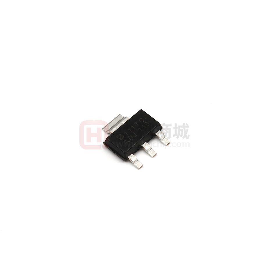
SOT-223 PKG
FEATURES
● Output Current up to 1 A
● Low Dropout Voltage ( 1.2V at 1A Output Current )
● Three Terminal Adjustable(ADJ) or Fixed 1.2V,1.5V, 1.8V, 2.5V, 2.85V, 3.3V, 5.0V ● Line Regulaion typically at 0.1% max ● Load Regulaion typically at 0.2% max ● Internal Current and Terminal Protection ● Maximum Input Voltage - 15V ● Surface Mount Package SOT-223, TO-252, SOT-89 ● 100% Thermal Limit Burn-In
TO-252 PKG
SOT-89 PKG
1
2
3
Pin 1. Adjust/Ground 2. Output 3. Input
APPLICATION
● ● ● ● ● ● ● Active SCSI Terminators Portable/Plan Top/Notebook Computers High Efficiency Linear Regulators SMPS Post Regulators Mother B/D Clock Supplies Disk Drives Battery Chargers
ORDERING INFORMATION
Device (Marking) Package LM1117S-ADJ SOT-223 LM1117S-XX LM1117RS-ADJ TO-252 LM1117RS-XX LM1117F-ADJ SOT-89 LM1117F-XX ( X.X=Output Voltage=1.2V,1.5V, 1.8V, 2.5V, '3.3V, 5.0V, Adjustable=ADJ)
DESCRIPTION
The LM1117 is a low power positive-voltage regulator designed to meet 1A output current and comply with SCSI-II specifications with a fixed output voltage of 2.85V. This device is an excellent choice for use in battery-powered applications, as active terminators for the SCSI bus, and portable computers. The LM1117 features very low quiescent current and very low dropout voltage of 1V at a full load and lower as output current decreases. LM1117 is available as an adjustable or fixed 1.5V, 1.8V, 2.5V, 3.3V, and 5.0V output voltages. The LM1117 is offered in a 3-pin surface mount package SOT-223, TO-252 & SOT-89. The output capacitor of 10㎌ or larger is needed for output stability of LM1117 as required by most of the other regulator circuits.
Jan. 2007 - Rev 1.0
HTC
1
�1A L.D.O. VOLTAGE REGULATOR
ABSOLUTE MAXIMUM RATINGS
CHARACTERISTIC DC Input Voltage Lead Temperature (Soldering, 5 Seconds) Storage Temperature Range Operating Junction Temperature Range SYMBOL VIN TSOL TSTG TOPR MIN.
LM1117S/RS/F
MAX. 15 260 150 125
-65 -40
UNIT V ℃ ℃ ℃
THERMAL DATA
PARAMETER Thermal Resistance Junction-Ambient SYMBOL SOT-223 TO-252 SOT-89 UNIT ℃/W
RθJA
130
93
315
TYPICAL APPLICATION
FIXED OUTPUT VOLTAGE
VIN 10㎌
Tantalum
LM1117S/RS/F
10㎌
Tantalum
Jan. 2007 - Rev 1.0
HTC
2
�1A L.D.O. VOLTAGE REGULATOR
(Refer to the test circuits, TJ=25℃ CO=10㎌ unless otherwise specified)
PARAMETER Reference Voltage Reference Voltage (TJ=0~125℃) Line Regulation Load Regulation SYMBOL VREF VREF ΔVO ΔVO ΔVO ΔVO VIN IADJ ΔIADJ IO(MIN) IO
EN
LM1117S/RS/F
ELECTRICAL CHARACTERISTICS FOR LM1117S/RS/F-ADJ(ADJUSTABLE)
TEST CONDITION
IO = 10mA to 1A, VIN - VO = 1.5 to 13.75V IO = 10mA to 1A, VIN - VO = 1.5 to 13.75V IO = 10mA , VIN - VO = 1.5 to 13.75V IO = 10mA to 1A, VIN - VO = 2 V
MIN. 1.238 1.219
TYP. 1.25 0.1 0.2 0.5 0.3
MAX. 1.262 1.281 0.2 0.4
UNIT V V % % % %
Temperature Stability Long Term Stability Operating Input Voltage Adjustment Pin Current Adjustment Pin Current Change Minimum Load Current Current Limit Output Noise (%VO) Supply Voltage Rejection
1000 hrs, T J = 125℃ VIN - VO = 1.5 to 12V IO = 100㎃ VIN - VO = 1.5 to 12V, I O = 10mA to 1A VIN - VO = 12V VIN - VO = 5V B = 10㎐ to 10㎑, TJ = 25℃ IO = 40㎃ , f = 120㎐, TJ = 25℃ VIN - V O = 3V, V NIPPLE = 1V PP IO = 100㎃ IO = 500㎃ IO = 1A TA = 25℃ 30㎳ Pulse 60 1000
15 50 0.5 5 1250 0.003 75 1.0 1.1 1.2
0.003
V ㎂ ㎂ ㎃ ㎃ % ㏈
120 5 10 1600
SVR
1.1 1.2 1.3
V V V %/W
Dropout Voltage Thermal Regulation
VD
(Refer to the test circuits, TJ=25℃ CO=10㎌ unless otherwise specified)
PARAMETER Output Voltage Output Voltage Line Regulation Load Regulation SYMBOL VO VO ΔVO ΔVO ΔVO ΔVO VIN ID IO
EN
ELECTRICAL CHARACTERISTICS FOR LM1117S/RS/F-1.2V
TEST CONDITION VIN = 3.2 I O = 0㎃ to 1A VIN=2.5 to 12V, I O=0㎃ to 1A (Tj = 0~125℃)
IO = 10mA , VIN - VO = 1.5 to 13.75V IO = 10mA to 1A, VIN - VO = 2 V
MIN. 1.176 1.152
TYP. 1.20 0.1 0.2 0.5 0.3
MAX. 1.224 1.248 0.2 0.4
UNIT V V % % % %
Temperature Stability Long Term Stability Operating Input Voltage Quiescent Current Current Limit Output Noise (%VO) Supply Voltage Rejection
1000 hrs, T J = 125℃ VIN - Vo = 5V VIN - VO = 5V B = 10㎐ to 10㎑, TJ = 25℃ IO = 40㎃ , f = 120㎐, TJ = 25℃ VIN - V O = 3V, V NIPPLE = 1V PP IO = 100㎃ IO = 500㎃ IO = 1A TA = 25℃ 30㎳ Pulse 60 1000
15 5 1250 0.003 75 1.0 1.1 1.2
0.003
V ㎃ ㎃ % ㏈
10 1600
SVR
1.1 1.2 1.3
V V V %/W
Dropout Voltage Thermal Regulation
VD
Jan. 2007 - Rev 1.0
HTC
3
�1A L.D.O. VOLTAGE REGULATOR
ELECTRICAL CHARACTERISTICS FOR LM1117
S/RS/F- 1.5
LM1117S/RS/F
(Refer to the test circuits, TJ=25℃ CO=10㎌ unless otherwise specified)
PARAMETER Output Voltage Output Voltage Line Regulation Load Regulation SYMBOL VO VO ΔVO ΔVO ΔVO ΔVO VIN ID IO
EN
TEST CONDITION VIN = 3.0 to 12V, I O = 0㎃ to 1A VIN=3.0 to 12V, I O=0㎃ to 1A (Tj = 0~125℃) VIN = 3.0 to 12V, I O = 0㎃ VIN = 3.5V, I O = 0 to 1A 1000 hrs, T J = 125℃ IO = 100㎃ VIN - Vo = 5V VIN - Vo = 5V B = 10㎐ to 10㎑, TJ = 25℃ IO = 40㎃ , f = 120㎐, TJ = 25℃ VIN = 5.5V, V NIPPLE = 1V PP IO = 100㎃ IO = 500㎃ IO = 1A TA = 25℃ 30㎳ Pulse
MIN. 1.485 1.470
TYP. 1.5 0.1 0.2 0.5 0.3 5
MAX. 1.515 1.530 0.2 0.4
UNIT V V % % % %
Temperature Stability Long Term Stability Operating Input Voltage Quiescent Current Current Limit Output Noise Voltage Supply Voltage Rejection
12 10 1600
V ㎃ ㎃ ㎶ ㏈
1000
1250 100
SVR
60
75 1.0 1.1 1.2 0.003 1.1 1.2 1.3
V V V %/W
Dropout Voltage Thermal Regulation
VD
ELECTRICAL CHARACTERISTICS FOR LM1117
S/RS/F- 1.8
(Refer to the test circuits, TJ=25℃ CO=10㎌ unless otherwise specified)
PARAMETER Output Voltage Output Voltage Line Regulation Load Regulation SYMBOL VO VO ΔVO ΔVO ΔVO ΔVO VIN ID IO
EN
TEST CONDITION VIN = 3.3 to 12V, I O = 0㎃ to 1A VIN=3.3 to 12V, I O=0㎃ to 1A (Tj = 0~125℃) VIN = 3.3 to 12V, I O = 10㎃ VIN = 3.8V, I O = 0 to 1A 1000 hrs, T J = 125℃ IO = 100㎃ VIN - Vo = 5V VIN - Vo = 5V B = 10㎐ to 10㎑, TJ = 25℃ IO = 40㎃ , f = 120㎐, TJ = 25℃ VIN = 5.5V, V NIPPLE = 1V PP IO = 100㎃ IO = 500㎃ IO = 1A TA = 25℃ 30㎳ Pulse
MIN. 1.782 1.764
TYP. 1.8 0.1 0.2 0.5 0.3
MAX. 1.818 1.836 0.2 0.4
UNIT V V ㎷ ㎷ % %
Temperature Stability Long Term Stability Operating Input Voltage Quiescent Current Current Limit Output Noise Voltage Supply Voltage Rejection
12 5 1000 1250 100 60 75 1.0 1.1 1.2 0.003 1.1 1.2 1.3 10 1600
V ㎃ ㎃ ㎶ ㏈ V V V %/W
SVR
Dropout Voltage Thermal Regulation
VD
Jan. 2007 - Rev 1.0
HTC
4
�1A L.D.O. VOLTAGE REGULATOR
LM1117S/RS/F
ELECTRICAL CHARACTERISTICS FOR LM1117
S/RS/F -2.5
(Refer to the test circuits, TJ=25℃ CO=10㎌ unless otherwise specified)
PARAMETER Output Voltage Output Voltage Line Regulation Load Regulation SYMBOL VO VO ΔVO ΔVO ΔVO ΔVO VIN ID IO
EN
TEST CONDITION VIN = 4.0 to 12V, I O = 0㎃ to 1A VIN=4.0 to 12V, I O=0㎃ to 1A (Tj = 0~125℃) VIN = 4.0 to 12V, I O = 10㎃ VIN = 4.5V, I O = 0 to 1A 1000 hrs, T J = 125℃ IO = 100㎃ VIN - Vo = 5V VIN - Vo = 5V B = 10㎐ to 10㎑, TJ = 25℃ IO = 40㎃ , f = 120㎐, TJ = 25℃ VIN = 5.5V, V NIPPLE = 1V PP IO = 100㎃ IO = 500㎃ IO = 1A TA = 25℃ 30㎳ Pulse
MIN. 2.475 2.450
TYP. 2.5 0.1 0.2 0.5 0.3 5
MAX. 2.525 2.550 0.2 0.4
UNIT V V % % % %
Temperature Stability Long Term Stability Operating Input Voltage Quiescent Current Current Limit Output Noise Voltage Supply Voltage Rejection
12 10 1600
V ㎃ ㎃ ㎶ ㏈
1000
1250 100
SVR
60
75 1.0 1.1 1.2 0.01 1.1 1.2 1.3 0.1
V V V %/W
Dropout Voltage Thermal Regulation
VD
ELECTRICAL CHARACTERISTICS FOR LM1117
S/RS/F -2.85
(Refer to the test circuits, TJ=25℃ CO=10㎌ unless otherwise specified)
PARAMETER Output Voltage Output Voltage Line Regulation Load Regulation SYMBOL VO VO ΔVO ΔVO ΔVO ΔVO VIN ID IO
EN
TEST CONDITION VIN = 4.4 to 12V, I O = 0㎃ to 1A VIN=4.4 to 12V, I O=0㎃ to 1A (Tj = 0~125℃) VIN = 4.4 to 12V, I O = 10㎃ VIN = 4.85V, I O = 0 to 1A 1000 hrs, T J = 125℃ IO = 100㎃ VIN - Vo = 5V VIN - Vo = 5V B = 10㎐ to 10㎑, TJ = 25℃ IO = 40㎃ , f = 120㎐, TJ = 25℃ VIN = 5.85V, V NIPPLE = 1V PP IO = 100㎃ IO = 500㎃ IO = 1A TA = 25℃ 30㎳ Pulse
MIN. 2.821 2.793
TYP. 2.85 0.1 0.2 0.5 0.3
MAX. 2.878 2.907 0.2 0.4
UNIT V V % % % %
Temperature Stability Long Term Stability Operating Input Voltage Quiescent Current Current Limit Output Noise Voltage Supply Voltage Rejection
12 5 1000 1250 100 60 75 1.0 1.1 1.2 0.003 1.1 1.2 1.3 10 1600
V ㎃ ㎃ ㎶ ㏈ V V V %/W
SVR
Dropout Voltage Thermal Regulation
VD
Jan. 2007 - Rev 1.0
HTC
5
�1A L.D.O. VOLTAGE REGULATOR
LM1117S/RS/F
ELECTRICAL CHARACTERISTICS FOR LM1117
S/RS/F -3.3
(Refer to the test circuits, TJ=25℃ CO=10㎌ unless otherwise specified)
PARAMETER Output Voltage Output Voltage Line Regulation Load Regulation SYMBOL VO VO ΔVO ΔVO ΔVO ΔVO VIN ID IO
EN
TEST CONDITION VIN = 4.8 to 12V, I O = 0㎃ to 1A VIN=4.8 to 12V, I O=0㎃ to 1A (Tj = 0~125℃) VIN = 4.8 to 12V, I O = 10㎃ VIN = 5.3V, I O = 0 to 1A 1000 hrs, T J = 125℃ IO = 100㎃ VIN - Vo = 5V VIN - Vo = 5V B = 10㎐ to 10㎑, TJ = 25℃ IO = 40㎃ , f = 120㎐, TJ = 25℃ VIN = 6.3V, V NIPPLE = 1V PP IO = 100㎃ IO = 500㎃ IO = 1A TA = 25℃ 30㎳ Pulse
MIN. 3.267 3.234
TYP. 3.3 0.1 0.2 0.5 0.3
MAX. 3.333 3.366 0.2 0.4
UNIT V V % % % %
Temperature Stability Long Term Stability Operating Input Voltage Quiescent Current Current Limit Output Noise Voltage Supply Voltage Rejection
12 5 1000 1250 100 60 75 1.0 1.1 1.2 0.003 1.1 1.2 1.3 10 1600
V ㎃ ㎃ ㎶ ㏈ V V V %/W
SVR
Dropout Voltage Thermal Regulation
VD
ELECTRICAL CHARACTERISTICS FOR LM1117
S/RS/F -5.0
(Refer to the test circuits, TJ=25℃ CO=10㎌ unless otherwise specified)
PARAMETER Output Voltage Output Voltage Line Regulation Load Regulation SYMBOL VO VO ΔVO ΔVO ΔVO ΔVO VIN ID IO
EN
TEST CONDITION VIN = 6.5 to 15V, I O = 0㎃ to 1A VIN=6.5 to 15V, I O=0㎃ to 1A (Tj = 0~125℃) VIN = 6.5 to 15V, I O = 10㎃ VIN = 7.0V, I O = 0 to 1A 1000 hrs, T J = 125℃ IO = 100㎃ VIN - Vo = 5V VIN - Vo = 5V B = 10㎐ to 10㎑, TJ = 25℃ IO = 40㎃ , f = 120㎐, TJ = 25℃ VIN = 6.3V, V NIPPLE = 1V PP IO = 100㎃ IO = 500㎃ IO = 1A TA = 25℃ 30㎳ Pulse
MIN. 4.950 4.900
TYP. 5.0 0.1 0.2 0.5 0.3
MAX. 5.050 5.100 0.2 0.4
UNIT V V % % % %
Temperature Stability Long Term Stability Operating Input Voltage Quiescent Current Current Limit Output Noise Voltage Supply Voltage Rejection
15 5 1000 1250 100 60 75 1.0 1.1 1.2 0.003 1.1 1.2 1.3 10 1600
V ㎃ ㎃ ㎶ ㏈ V V V %/W
SVR
Dropout Voltage Thermal Regulation
VD
Jan. 2007 - Rev 1.0
6
HTC
�1A L.D.O. VOLTAGE REGULATOR
LM1117S/RS/F
APPLICATION CIRCUITS
Figure 1.
Figure 2.
VIN C1
IN
LM1117
ADJ
VIN
OUT
IN
LM1117
ADJ IADJ 50㎂
OUT
VOUT C2
C1 R1 VREF R1
LOAD
VOUT=VREF(1+R2/R1)+IADJR2
R2
1A Current Output
Typical Adjustable Regulator
Figure 3. Negative Supply
VIN +
LM1117S-50 IN OUT GND
10㎌
+
100㎌
VOUT=-5V
FLOATING INPUT
Jan. 2007 - Rev 1.0
HTC
7
�1A L.D.O. VOLTAGE REGULATOR
LM1117S/RS/F
Figure 4. Active Terminator for SCSI-2 BUS
110 110
+
4.75V TO 5.25V
LM1117S-28 IN (2.85V) GND
10㎌
110 + 22㎌ 110
18-27 LINES
Figure 5. Voltage Regulator With Reference
VIN>11.5V 10㎌
+
LM1117S-50 IN OUT GND
5VOUT
10V + 100㎌
Jan. 2007 - Rev 1.0
HTC
8
�1A L.D.O. VOLTAGE REGULATOR
LM1117S/RS/F
Figure 6. Battery Backed-up Regulated Supply
VIN 10㎌
+
LM1117S-50 IN OUT GND
50Ω
5.2V LINE 5.0 BATTERY
SELECT FOR CHARGE VALUE
+ 6.5V 10㎌
LM1117S-50 IN OUT GND
+ 100㎌
* NOTES : IF ANYTHING WILL BE CHANGED FOR THIS SPECIFICATION, TAEJIN TECHNOLOGY MUST INFORM PCC BEFORE THE CHANGE
Jan. 2007 - Rev 1.0
HTC
9
�1A L.D.O. VOLTAGE REGULATOR
Typical Performance Characteristics
2.0 Vout, OUTPUT VOLTAGE CHANGE(%) Vin-Vout DROPOUT VOLTAGE (V) , 1.5 1.0 Adj,1.5V,1.8V,2.5V 0.5 0 -0.5 -1.0 -1.5 -2.0 -50 -25 -0 25 50 75 100 TA-FREE-AIR TEMPERATURE-℃ 125 150 5.0V Vin=Vout +3.0V Iout=10mA 1.6 1.4 1.2 1.0 0.8 0.6 0.4 0.2 0 0 100 Tj = -40℃ Tj = 25℃ Tj = 125℃
LM1117S/RS/F
300 200 400 500 600 Iout, OUTPUT CURRENT(mA)
800
1000
FIG 1. OUTPUT VOLTAGE CHANGE vs TEMPERATURE(℃)
FIG 2. DROPOUT VOLTAGE vs OUTPUT CURRENT
2.0 Tj = 25℃ Iout, OUTPUT CURRENT(A)
1.8 1.7 Vin=Vout +3.0V Iout=10mA
1.5
Iout, OUTPUT CURRENT(A)
1.6 1.5 1.4 1.3 1.2 1.1 Vin = 5.0 V Load pulsed at 1.0% duty cycle
1.0
0.5
0 0 2 4 6 8 10 12 1 16 18 20
1.0 -50 -25 -0 25 50 75 100 TA- AMBIENT TEMPERATURE (℃) 125 150
Vin - Vout, VOLTAGE DIFFERENTIAL (V)
FIG 3. OUTPUT SHORT CIRCUIT CURRENT vs DIFFERENTIAL VOLTAGE
FIG 4. OUTPUT SHORT CIRCUIT CURRENT vs TEMPERATURE
IQ, QUIESCENT CURRENT CHANGE (%
20 15 10 5
Iadj, ADJUST PIN CURRENT
Iout = 10 mA 60 50 40
0 -5 -10 -15
10 -50 -25 -0 25 50 75 100 125 150
-20 -50 -25 -0 25 50 75 100 125 150
TA, AMBIENT TEMPERATURE (℃)
TA, AMBIENT TEMPERATURE(℃)
FIG 5. ADJ PIN CURRENT vs TEMPERATURE (℃)
FIG 6. QUIESCENT CURRENT CHANGE vs TEMPERATURE (℃)
Jan. 2007 - Rev 1.0
HTC
10
�1A L.D.O. VOLTAGE REGULATOR
Maximum Output Current Capability
LM1117S/RS/F
The LM1117 can deliver a continuous current of 1A over the full operating junction temperature range. However, the current is limited by the restriction of power dissipation which differs from packages. A heat sink may be required depending on the maximum power dissipation and maximum ambient temperature of application. With respect to th applied package, the maximum output current of 1A may be still undeliverable due to the restriction of the power diss of LM1117. Under all possible conditions, the junction temperature must be within the range specified under operating conditions. The temperatures over the device are given by: TC = T A + PD X θCA TJ = T C + PD X θJC TJ = T A + PD X θJA TJ is the junction temperature, T C is the case temperature, TA is the ambient temperature, P D is the total power dissi of the device, θCA is the thermal resistance of case-to-ambient, θJC is the thermal resistance of junction-to-case, and θJA is the thermal resistance of junction to ambient. The total power dissipation of the device is given by PD = PIN – POUT = (VIN X IIN)–(VOUT X IOUT) = (VIN X (IOUT+IGND)) – (VOUT X IOUT) = (VIN - VOUT) X IOUT + VIN X IGND where IGND is the operating ground current of the device which is specified at the Electrical Characteristics. The max allowable temperature rise (TRmax) depends on the maximum ambient temperature (TAmax) of the application and the maximum allowable junction temperature (TJmax): TRmax = T Jmax – TAmax The maximum allowable value for junction-to-ambient thermal resistance, θ JA, can be calculated using the formula: θJA = T Rmax / PD LM1117 is available in SOT223, TO252 packages. The thermal resistance depends on amount of copper area or he and on air flow. If the maximum allowable value of θJA calculated above is over 130°C/W for SO-223 package, over for TO252 package, no heat sink is needed since the package can dissipate enough heat to satisfy these requirements. If the value for allowable θJA falls near or below these limits, a heat sink or proper area of cop plane is required. In summary, the absolute maximum ratings of thermal resistances are as follow:
Absolute Maximum Ratings of Thermal Resistance Characteristic Symbol Thermal Resistance Junction-To-Ambient / SOT223 θJA-SOT223 Thermal Resistance Junction-To-Ambient / TO252 θJA-TO252 Thermal Resistance Junction-To-Ambient / SOT89 θJA-SOT89 2 No heat sink / No air flow / No adjacent heat source / 0.066 inch copper area
Max. Rating 130 93 315
Unit °C/W °C/W °C/W
Jan. 2007 - Rev 1.0
HTC
11
�