1A Low-Voltage Low-Dropout Regulator
LM39100/39101/39102
FEATURES
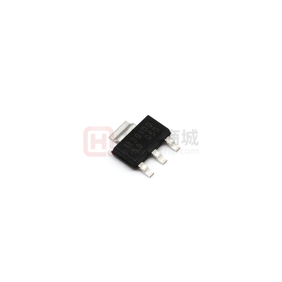
SOT-223 PKG
Fixed and adjustable output voltages to 1.24V
410mV typical dropout at 1A
Ideal for 3.0V to 2.5V conversion
Ideal for 2.5V to 1.8V or 1.5V conversion
1A minimum guaranteed output current
1% initial accuracy
Low ground current
Current limiting and thermal shutdown
Reversed-battery protection
Reversed-leakage protection
Fast transient response
Low-profile SOT-223 package
Moisture Sensitivity Level 3
TO-252 3L / 5L PKG
SOP-8 PKG
ORDERING INFORMATION
Device
LM39100S-X.X
LM39100GS-X.X
LM39100RS-X.X
LM39100GRS-X.X
LM39101RS-X.X
LM39101GRS-X.X
LM39102RS
LM39102GRS
LM39101D-X.X
LM39102D
APPLICATION
Battery Powered Equipments
Motherboards and Graphic Cards
Microprocessor Power Supplies
Peripheral Cards
High Efficiency Linear Regulators
Battery Chargers
DESCRIPTION
Package
SOT-223
TO-252 3L
TO-252 5L
SOP-8
X.X = Output Voltage = 1.5, 1.8, 2.5, 3.3, 5.0
The LM39100/1/2 is 1A low-dropout linear voltage
regulators that provide low-voltage, high-current output.
The LM39100/1/2 offers extremely low dropout (typically 410mV at 1A) and low ground current (typically 12mA
at 1A). The LM39100 is a fixed output regulator offered in the SOT-223 package. The LM39101 and LM39102
are fixed and adjustable regulators, respectively, in SOP-8 and TO-252 Packages.
The LM39100/1/2 is ideal for PC add-in cards that need to convert from standard 5V to 3.3V, 3.3V to 2.5V or
2.5V to1.8V. A guaranteed maximum dropout voltage of 630mV overall operating conditions allows the
LM39100/1/2 to provide2.5V from a supply as low as 3.13V and 1.8V from a supply as low as 2.43V. The
LM39100/1/2 is fully protected with over current limiting, thermal shutdown, and reversed-battery protection.
Fixed voltages of 5.0V, 3.3V, 2.5V, 1.8V and 1.5V are available on LM39100/1 with adjustable output voltages
to 1.24V on LM39102.
Absolute Maximum Ratings (Note 1)
CHARACTERISTIC
SYMBOL
MIN.
MAX.
UNIT
Supply Voltage
VIN
- 0.3
+ 20
V
Enable Voltage
VEN
-
+ 20
V
Output Voltage
VOUT
-0.3
VIN +0.3
V
Lead Temperature (Soldering, 5 sec)
TSOL
-
260
℃
Storage Temperature Range
TSTG
-65
+ 150
℃
Feb. 2012 - Rev. 1.5.3
-1
-
HTC
�1A Low-Voltage Low-Dropout Regulator
LM39100/39101/39102
Operating Ratings (Note 2)
CHARACTERISTIC
SYMBOL
MIN.
MAX.
UNIT
Supply Voltage
VIN
+ 2.25
+ 16
V
Enable Voltage
VEN
+ 2.25
+ 16
V
PD(max)
(Note 3)
(Note 3)
TJ
-40
+ 125
Maximum Power Dissipation
Junction Temperature
Package Thermal Resistance
℃
θJA-SOT-223
115
℃/W
θJA-TO252
95
℃/W
θJA-SOP-8
130
℃/W
Ordering Information
VOUT
1.5 V
1.8 V
2.5 V
3.3 V
Package
Order No.
Description
Supplied As
Status
SOT-223
LM39100S-1.5V
1A, Fixed
Reel
Active
SOT-223
LM39100GS-1.5V
1A, Fixed
Reel
Contact us
TO-252 3L
LM39100RS-1.5V
1A, Fixed
Reel
Active
TO-252 3L
LM39100GRS-1.5V
1A, Fixed
Reel
Active
TO-252 5L
LM39101RS-1.5V
1A, Fixed, Enable
Reel
Active
TO-252 5L
LM39101GRS-1.5V
1A, Fixed, Enable
Reel
Active
SOP-8
LM39101D-1.5V
1A, Fixed, Enable
Reel
Active
SOT-223
LM39100S-1.8V
1A, Fixed
Reel
Active
SOT-223
LM39100GS-1.8V
1A, Fixed
Reel
Contact us
TO-252 3L
LM39100RS-1.8V
1A, Fixed
Reel
Active
TO-252 3L
LM39100GRS-1.8V
1A, Fixed
Reel
Active
TO-252 5L
LM39101RS-1.8V
1A, Fixed, Enable
Reel
Active
TO-252 5L
LM39101GRS-1.8V
1A, Fixed, Enable
Reel
Active
SOP-8
LM39101D-1.8V
1A, Fixed, Enable
Reel
Active
SOT-223
LM39100S-2.5V
1A, Fixed
Reel
Active
SOT-223
LM39100GS-2.5V
1A, Fixed
Reel
Contact us
TO-252 3L
LM39100RS-2.5V
1A, Fixed
Reel
Active
TO-252 3L
LM39100GRS-2.5V
1A, Fixed
Reel
Active
TO-252 5L
LM39101RS-2.5V
1A, Fixed, Enable
Reel
Active
TO-252 5L
LM39101GRS-2.5V
1A, Fixed, Enable
Reel
Active
SOP-8
LM39101D-2.5V
1A, Fixed, Enable
Reel
Active
SOT-223
LM39100S-3.3V
1A, Fixed
Reel
Active
SOT-223
LM39100GS-3.3V
1A, Fixed
Reel
Contact us
TO-252 3L
LM39100RS-3.3V
1A, Fixed
Reel
Active
TO-252 3L
LM39100GRS-3.3V
1A, Fixed
Reel
Active
TO-252 5L
LM39101RS-3.3V
1A, Fixed, Enable
Reel
Active
TO-252 5L
LM39101GRS-3.3V
1A, Fixed, Enable
Reel
Active
SOP-8
LM39101D-3.3V
1A, Fixed, Enable
Reel
Active
Feb. 2012 - Rev. 1.5.3
-2
-
HTC
�1A Low-Voltage Low-Dropout Regulator
LM39100/39101/39102
Ordering Information
VOUT
5.0 V
ADJ
Package
Order No.
Description
Supplied As
Status
SOT-223
LM39100S-5.0V
1A, Fixed
Reel
Active
SOT-223
LM39100GS-5.0V
1A, Fixed
Reel
Contact us
TO-252 3L
LM39100RS-5.0V
1A, Fixed
Reel
Active
TO-252 3L
LM39100GRS-5.0V
1A, Fixed
Reel
Active
TO-252 5L
LM39101RS-5.0V
1A, Fixed, Enable
Reel
Active
TO-252 5L
LM39101GRS-5.0V
1A, Fixed, Enable
Reel
Active
SOP-8
LM39101D-5.0V
1A, Fixed, Enable
Reel
Active
TO-252 5L
LM39102RS
1A, Adjustable, Enable
Reel
Active
TO-252 5L
LM39102GRS
1A, Adjustable, Enable
Reel
Active
SOP-8
LM39102D
1A, Adjustable, Enable
Reel
Active
LM 3910X
Output Voltage : 1.5V / 1.8V / 2.5V / 3.3V / 5.0V / Blank(ADJ Only)
S : SOT-223
RS : TO-252
D : SOP-8
Package Type
Green Mode
G
: Halogen Free
Blank : Pb Free
Root Name
39100 : 3L Fixed Output
39101 : 5L Fixed Output
39102 : 5L / 8L Adjustable Output
Product Code
Feb. 2012 - Rev. 1.5.3
-3
-
HTC
�1A Low-Voltage Low-Dropout Regulator
LM39100/39101/39102
PIN CONFIGURATION
EN
1
8
GND
VIN
2
7
GND
VOUT
3
6
GND
FLG/ADJ 4
5
GND
SOP-8
VOUT
3
2
GND (TAB)
2
GND (TAB)
1
VIN
1
VIN
SOT-223
5
FLG/ADJ
4
VOUT
3
GND (TAB)
2
VIN
1
EN
VOUT
3
TO-252 3L
TO-252 5L
PIN DESCRIPTION
SOT-223 & TO-252 3L (for 39100)
Pin No.
Name
Function
1
VIN
Input Supply
2
GND
Ground
3
VOUT
Output Voltage
TO-252 5L (for 39101/2)
SOP-8 (for 39101/2)
Pin No.
Name
Function
Name
Function
1
EN
Chip Enable
EN
Chip Enable
2
VIN
Input Supply
VIN
Input Supply
3
GND
Ground
VOUT
Output Voltage
4
VOUT
Output Voltage
FLG / ADJ
Error Flag Output
or Output Adjust
5
FLG / ADJ
Error Flag Output
or Output Adjust
GND
Ground
6/7/8
-
-
GND
Ground
Feb. 2012 - Rev. 1.5.3
-4
-
HTC
�1A Low-Voltage Low-Dropout Regulator
LM39100/39101/39102
TYPICAL APPLICATION
100k
Error Flag
Output
LM39100
3.3V
IN
LM39101
2.5V
OUT
3.3V
GND
IN
Enable
Shutdown
2.5V / 1A Regulator
EN
OUT
GND
2.5V
FLG
2.5V / 1A Regulator with Error Flag
LM39102
2.5V
Enable
Shutdown
IN
EN
1.5V
OUT
GND
ADJ
R1
R2
1.5V / 1A Adjustable Regulator
Feb. 2012 - Rev. 1.5.3
-5
-
HTC
�1A Low-Voltage Low-Dropout Regulator
LM39100/39101/39102
ELECTRICAL CHARACTERISTICS
VIN= VOUT +1V; VEN = 2.25V; TJ = 25°C, bold values indicate -40°C ≤ TJ ≤ +125°C; unless noted
Symbol
VOUT
ΔVOUT/ΔT
Parameters
Condition
Min.
IOUT(lim)
Unit
1
2
%
%
10mA
10mA ≤ IOUT ≤ 1A, VOUT+1V ≤ VIN ≤8V
Line Regulation
IOUT=10mA, VOUT +1V ≤ VIN ≤ 16V
0.06
0.5
%
Load Regulation
VIN= VOUT +1V, 10mA ≤ IOUT ≤ 1A
0.2
1
%
40
100
ppm/ °C
150
200
250
mV
mV
-1
-2
Output Voltage Temp.
Coefficient (Note 4)
Dropout Voltage (Note 5)
IOUT=500mA, ΔVOUT = -1%
275
IOUT=750mA, ΔVOUT = -1%
330
500
mV
410
550
630
mV
mV
IOUT=1A, ΔVOUT = -1%
IGND
Max.
Output Voltage
IOUT=100mA, ΔVOUT = -1%
VDO
Typ.
Ground Current (Note 6)
Current Limit
mV
IOUT=100mA, VIN= VOUT+1V
700
μA
IOUT=500mA, VIN= VOUT+1V
4
mA
IOUT=750mA, VIN= VOUT+1V
7
mA
VOUT=0V, VIN=VOUT+1V
1.3
2.5
3.5
A
0.8
V
Enable Input
logic low (off)
VEN
Enable Input Voltage
logic high (on)
2.25
1
15
30
75
2
4
IOUT =10mA, VIN =VOUT +1V,
VEN =0V to VIN
50
500
IOUT =500mA, VIN =VOUT +1V,
VEN =0V to VIN
250
2000
IOUT =1.0A, VIN =VOUT +1V,
VEN =0V to VIN
350
3000
0.01
1
2
300
400
VEN=2.25V
IEN
V
Enable Input Current
VEN=0.8V
TEN
Delay time to
Nominal Output Voltage
(Note 7)
μA
μA
μA
μA
μs
Flag Output
IFLG (leak)
VFLG (do)
VFLG
Output Leakage
Current
Output Low Voltage
VOH=16V
(Note 8)
VIN=0.9.VOUT NOMINAL, IOL=250μA
Low Threshold
% of VOUT
High Threshold
% of VOUT
93
%
99.2
Hysteresis
Feb. 2012 - Rev. 1.5.3
240
1
-6
-
μA
μA
mV
mV
%
%
HTC
�1A Low-Voltage Low-Dropout Regulator
LM39100/39101/39102
LM39102 Only
1.228
1.215
Reference Voltage
(Note 9)
1.24
1.203
40
Adjust Pin Bias
Current
Reference Voltage
Temp. Coefficient (Note 4)
20
Adjust Pin Bias Current
Temp. Coefficient
0.1
1.252
1.265
V
V
1.277
V
80
120
nA
nA
ppm/ °C
99.2
nA/ °C
Note 1. Exceeding the absolute maximum ratings may damage the device.
Note 2. The device is not guaranteed to function outside its operating rating.
Note 3. PD (max)= (TJ (max) - TA) ÷ θJA, where θJA -junction-to-ambient thermal resistance.
Note 4. Output voltage temperature coefficient is ΔVOUT (worst case) ÷ (TJ(max) - TJ(min)) where TJ(max) is +125°C and TJ(min) is 0°C.
Note 5. VDO = VIN - VOUT when VOUT decreases to 99% of its nominal output voltage with VIN = VOUT + 1V. For output voltages below 2.25V,
dropout voltage is the input-to-output voltage differential with the minimum input voltage being 2.25V. Minimum input operating voltage
is 2.25V.
Note 6. IGND is the quiescent current. IIN = IGND + IOUT.
Note 7. Delay time is measured after VEN=VIN.
CIN=COUT=10μF.
Note 8. For adjustable device and fixed device with VOUT ≥ 2.5V
Note 9. VREF ≤ VOUT ≤ (VIN - 1V), 2.25V ≤ VIN ≤ 16V, 10mA ≤ IL ≤ 1 A.
Feb. 2012 - Rev. 1.5.3
-7
-
HTC
�1A Low-Voltage Low-Dropout Regulator
LM39100/39101/39102
TYPICAL OPERATING CHARACTERISTICS
Feb. 2012 - Rev. 1.5.3
-8
-
HTC
�1A Low-Voltage Low-Dropout Regulator
LM39100/39101/39102
TYPICAL OPERATING CHARACTERISTICS
Feb. 2012 - Rev. 1.5.3
-9
-
HTC
�1A Low-Voltage Low-Dropout Regulator
LM39100/39101/39102
APPLICATION INFORMATION
The LM39100/1/2 is a high-performance low-dropout voltage regulator suitable for moderate to high-current
voltage regulator applications. Its 630mV dropout voltage at full load and over temperature makes it especially
valuable in battery-powered systems and as high-efficiency noise filters in post-regulator applications. Unlike
older NPN-pass transistor de-signs, where the minimum dropout voltage is limited by the base-to-emitter
voltage drop and collector-to-emitter saturation voltage, dropout performance of the PNP output of these
devices is limited only by the low VCE saturation voltage. A trade-off for the low dropout voltage is a varying
base drive requirement.
The LM39100/1/2 regulator is fully protected from damage due to fault conditions. Linear current limiting is
provided. Output current during overload conditions is constant. Thermal shutdown disables the device when
the die temperature exceeds the maximum safe operating temperature. Transient protection allows device
(and load) survival even when the input voltage spikes above and below nominal. The output structure of
these regulators allows voltages in excess of the desired output voltage to be applied without reverse current
flow.
Output Capacitor
The LM39100/1/2 requires an output capacitor to maintain stability and improve transient response. Proper
capacitor selection is important to ensure proper operation. The LM39100/1/2 output capacitor selection is
dependent upon the ESR (equivalent series resistance) of the output capacitor to maintain stability. When
the output capacitor is 10μF or greater, the output capacitor should have an ESR less than 2Ω. This will
improve transient response as well as promote stability. Ultra-low ESR capacitors (