Low-Power, Slew-Rate-Limited RS-485/RS-422 Transceivers
MAX485
DESCRIPTION
The MAX485 is a half-duplex transceiver that meets the
specifications of RS-485 and RS-422. Its BiCMOS
design allows low power operation without sacrificing
performance. The MAX485 meets the requirements of
the RS-485 and RS-422 protocols up to 5Mbps
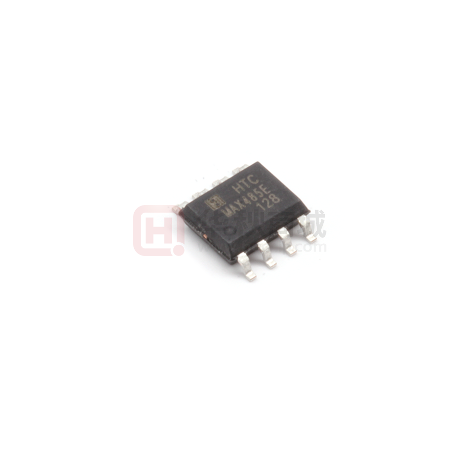
SOP-8
underload. The ESD tolerance is more than ±8kV for
both Human Body Model and ±15kV for IEC61000-4-2
DIP-8
Air Discharge Method on this device.
FEATURES
• Single +5V Supply
• Low Power BiCMOS
• Driver/Receiver Enable for Multi-Drop Configurations
• Half-Duplex Versions Available
• Data rate: 5 Mbps
• ESD Specifications
TRUTH TABLE
- ±15kV IEC61000-4-2 Air Discharge
Transmission
- ±8kV Human Body Model
Inputs
APPLICATIONS
• Low Power RS-485 Systems
• DTE-DCE Interface
• Packet Switching
• Local Area Networks
• Data Concentration
• Data Multiplexers
• Integrated Services Digital Network (ISDN)
R
7
B
DE 3
6
A
4
Apr. 2019_R1.1
D
DE
DI
A
B
X
1
1
1
0
X
1
0
0
1
0
0
X
Z
Z
1
0
X
Z
Z
Receiver
Outputs
RE
DE
A-B
RO
0
0
≥ +0.2V
1
0
0
≤ -0.2V
0
0
0
Open
1
1
0
X
Z
8 VCC
RE 2
DI
RE
Inputs
PIN CONFIGRUATION AND LOGIC DIAGRAM
RO 1
Outputs
5 GND
1 /10
HTC
�Low-Power, Slew-Rate-Limited RS-485/RS-422 Transceivers
MAX485
ORDERING INFORMATION
Package
Oder No.
Description
Marking
Compliance
Status
SOP-8
MAX485ED
RS-485/RS-422 Transceivers
MAX485E
RoHS, Green
Active
DIP-8
MAX485EN
RS-485/RS-422 Transceivers
MAX485E
RoHS, Green
Contact us
MAX
485
Package Type
D
N
: SOP-8
: DIP-8
Ambient Temperature
E
: -40℃ ~ 85℃
Root Name
Product Code
Apr. 2019_R1.1
2 /10
HTC
�Low-Power, Slew-Rate-Limited RS-485/RS-422 Transceivers
MAX485
ABSOLUTE MAXIMUM RATINGS
Characteristic
Symbol
Supply Voltage
Min
VCC
Max
Unit
7
V
Control Input Voltage
VDE, VRE
-0.3
VCC + 0.5
V
Driver Input Voltage
VDI
-0.3
VCC + 0.5
V
Driver Output Voltage
A, B
-15
15
V
Receiver Input Voltage
A, B
-15
15
V
Receiver Output Voltage
VRO
-0.3
VCC + 0.5
V
TJ
-40
125
°C
TSTG
-65
150
°C
Symbol
Min
Max
Unit
Supply Voltage
VCC
4.75
5.25
V
Operating Ambient Temperature Ranges
TA
-40
85
°C
Junction Temperature
Storage Temperature Range
RECOMMENDED OPERATING CONDITIONS
Characteristic
Apr. 2019_R1.1
3 /10
HTC
�Low-Power, Slew-Rate-Limited RS-485/RS-422 Transceivers
MAX485
PIN CONFIGURATION
1
2
8
1
7
2
8
7
MAX485EN
MAX485ED
3
6
3
6
4
5
4
5
SOP-8
DIP-8
PIN DESCRIPTION
SOP-8 / DIP-8 PKG
Pin No.
Function
Name
1
RO
Receiver Output
2
RE*
Receiver Output Enable Active Low
3
DE
Driver Output Enable Active High
4
DI
Driver Input
5
GND
6
A
Non-inverting Driver Output and Receiver Input
7
B
Inverting Driver Output and Receiver Input
8
VCC
Apr. 2019_R1.1
Ground
Power Supply: 4.75V to 5.25V
4 /10
HTC
�Low-Power, Slew-Rate-Limited RS-485/RS-422 Transceivers
MAX485
ELECTRICAL CHARACTERISTICS
Unless otherwise specified: VCC = 5V ± 5%, TA = TMIN to TMAX
PARAMETER
DRIVER DC Characteristics
Differential Driver Output
(no load)
Differential Driver Output
(with load)
Change in Magnitude of Driver
Differential Output Voltage for
Complementary Output States
Driver Common-Mode Output Voltage
Change in Magnitude of Driver
Common-Mode Output Voltage for
Complementary Output States
Input High Voltage
Input Low Voltage
Input Current
Driver Short Circuit Current
Driver Short-Circuit Current,
VO = High
Driver Short-Circuit Current,
VO = Low
DRIVER AC Characteristics
Max. Transmission Rate
Driver Input to Output
Driver Output Skew to Output
Driver Rise or Fall Time
Driver Enable to Output High
Driver Enable to Output Low
Driver Disable Time from Low
Driver Disable Time from High
RECEIVER DC Characteristics
Receiver Differential Threshold
Voltage
Receiver Input Hysteresis
Receiver Output High Voltage
Receiver Output Low Voltage
Three-State (High Impedance) Output
Current at Receiver
Receiver Input Resistance
Symbol
MAX
UNITS
GND
VCC
V
2
1.5
VCC
VCC
V
MIN
TYP
VOD1
RL = ∞, Figure 1
VOD2
RL = 50Ω (RS-422), Figure 1
RL = 27Ω (RS-485), Figure 1
ΔVOD
RL = 27Ω or 50Ω, Figure 1
0.2
V
VOC
RL = 27Ω or 50Ω, Figure 1
3
V
ΔVOC
R = 27Ω or 50Ω, Figure 1
0.2
V
0.8
±10
V
V
uA
VIH
VIL
IIN1
DE, DI, RE*
DE, DI, RE*
DE, DI, RE*
2.0
IOSD1
-7V ≤ VO ≤ 12V
±250
mA
IOSD2
-7V ≤ VO ≤ 12V
±250
mA
60
60
10
40
70
70
70
70
Mbps
ns
ns
ns
ns
ns
ns
ns
ns
0.2
V
0.4
mV
V
V
±1
uA
fMAX
tDPLH
tDPHL
tSKEW
tr , tf
tZH
tZL
tHZ
tLZ
VTH
5
Figure 4 & 6
CL=100pF
S2 closed
S1 closed
S2 closed
S1 closed
-7V ≤ VCM ≤ 12V
-0.2
VCM = 0V
IO = -4mA, VID = +200mV
IO = +4mA, VID = -200mV
IOZR
0.4V ≤ VO ≤ 2.4V, RE* = 5V
RIN
-7V ≤ VCM ≤ 12V
IIN2
Receiver Short-Circuit Current
IOSR
30
30
5
15
40
40
40
40
Figure 3 & 5
RL = 54Ω, CL1 = CL2 = 100pF
ΔVTH
VOH
VOL
Input Current (A, B)
Apr. 2019_R1.1
CONDITIONS
DE = 0V
VCC = 0V or 5.25V
0V ≤ VO ≤ VCC
5 /10
20
3.5
12
VIN = 12V
VIN = -7V
7
kΩ
15
1.0
-0.8
95
mA
mA
HTC
�Low-Power, Slew-Rate-Limited RS-485/RS-422 Transceivers
MAX485
RECEIVER AC Characteristics
Receiver Input to Output
| tPLH - tPHL | Differential
Receiver Skew
Receiver Enable to Output Low
Receiver Enable to Output High
Receiver Disable Time from Low
Receiver Disable Time from High
Supply Current
No-Load Supply Current
Apr. 2019_R1.1
tPLH
tPHL
tSKD
20
20
Figure 2 & 7
S1, S2 open
CL = 15pF
45
45
13
tZL
tZH
tLZ
tHZ
Figure 2 & 8
CL = 15pF
S1 closed
S2 closed
S1 closed
S2 closed
45
45
45
45
ICC
RE = 0V or VCC
DE=VCC
DE=0V
900
600
6 /10
100
100
ns
ns
ns
70
70
70
70
ns
ns
ns
Ns
uA
HTC
�Low-Power, Slew-Rate-Limited RS-485/RS-422 Transceivers
MAX485
TEST CIRCUITS
A
VCC
RO
RL
S1
Receiver
Output
VOD
RL
1kΩ
VOC
S2
CL
B
Figure1.
Figure 2.
VCC
CL1
DI
D
Output
Under
Test
RL VO
S1
500Ω
CL
CL2
DE
Figure 3.
S2
Figure 4.
tSKEW = |tDPLH – tDPHL|
3V
Driver
Input
1.5V
1.5V
0V
tDPLH
tDPHL
Z
1/2VO
Driver
Output
1/2VO
VO
Y
VO
Differential
Output
90%
90%
0V
VDIFF=V(Y) - V(Z)
-VO
10%
10%
tR
tF
Figure 5.
Apr. 2019_R1.1
7 /10
HTC
�Low-Power, Slew-Rate-Limited RS-485/RS-422 Transceivers
MAX485
3V
1.5V
DE
1.5V
0V
tLZ
tZL
Y, Z
2.3V
A, B
VOL + 0.5V
VOL
VOH
Y, Z
VOH – 0.5V
2.3V
A, B
0V
tZH
tHZ
Figure 6.
VOH
RO
1.5V
1.5V
OUTPUT
VOL
tPLH
tPHL
VOD2+
A-B
0V
0V
INPUT
VOD2-
Figure 7.
3V
1.5V
RE*
1.5V
0V
tLZ
tZL
VCC
1.5V
VOL + 0.5V
RO
VIL
VIH
VOH – 0.5V
1.5V
0V
tZH
tHZ
Figure 8.
Apr. 2019_R1.1
8 /10
HTC
�Low-Power, Slew-Rate-Limited RS-485/RS-422 Transceivers
MAX485
APPLICATION INFORMATION
FUNCTIONAL DESCRIPTION
The MAX485 is half-duplex differential transceiver that meets the requirements of RS-485 and RS-422.
The RS-485 standard is ideal for multi-drop applications and for long-distance interfaces. RS-485 allows
up to 32 drivers and 32 receivers to be connected to a data bus, making it an ideal choice for multi-drop
applications. Since the cabling can be as long as 4,000 feet, RS-485 transceivers are equipped with a
wide (-7V to +12V) common mode range to accommodate ground potential differences. Because RS-485
is a differential interface, data is virtually immune to noise in the transmission line.
DRIVERS
The driver outputs of the MAX485 are differential outputs meeting the RS-485 and RS-422 standards.
The typical voltage output swing with no load will be 0 Volts to +5 Volts. With worst case loading of 54Ω
across the differential outputs, the drivers can maintain greater than 1.5V voltage levels. The drivers of
the MAX485 have an enable control line which is active HIGH. A logic HIGH on DE (pin 3) will enable the
differential driver outputs. A logic LOW on the DE(pin 3) will tri-state the driver output. The transmitters of
the MAX485 will operate up to at least 5Mbps.
RECEIVERS
The MAX485 receiver has differential inputs with an input sensitivity as low as ±200mV. Input impedance
of the receivers is typically 15kΩ (12kΩ minimum). A wide common mode range of -7V to +12V allows for
large ground potential differences between systems. The receivers of the MAX485 have a tri-state enable
control pin. A logic LOW on RE* (pin 2) will enable the receiver, a logic HIGH on RE*(pin 2) will disable
the receiver. The receiver for the MAX485 will operate up to at least 5Mbps. The receiver is equipped
with the fail-safe feature. Fail-safe guarantees that the receiver output will be in a HIGH state when the
input is left unconnected.
Apr. 2019_R1.1
9 /10
HTC
�Low-Power, Slew-Rate-Limited RS-485/RS-422 Transceivers
MAX485
REVISION NOTICE
The description in this datasheet can be revised without any notice to describe its electrical characteristics properly.
Apr. 2019_R1.1
10 /10
HTC
�