DC-DC Converter Control Circuits
FEATURES
● OUTPUT SWITCH CURRENT IN EXCESS OF 1.5A ● 2% REFERENCE ACCURACY ● LOW QUIESCENT CURRENT:2.5mA(TYP.) ● OPERATING FROM 3V TO 40V ● FREQUENCY OPERATION TO 100KHz ● ACTIVE CURRENT LIMITING ● MOISTURE SENSITIVITY LEVEL 3 ●
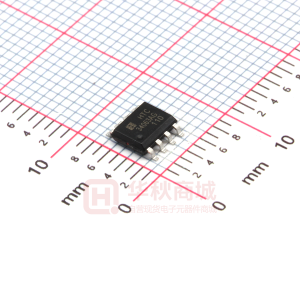
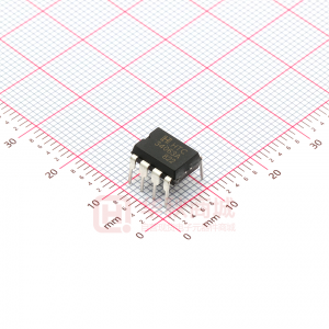
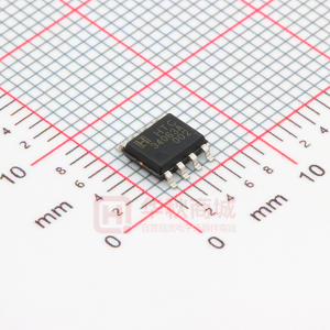
MC34063A
8 SOP/ 8 DIP PIN Configulation
MC34063AG is Halogen Free products
SOP-8 PKG DIP-8 PKG
APPLICATION
● Battery Chargers ● NICs / Switches / Hubs ● ADSL Modems ● Negative Voltage Power Supplies
Switch Collector Switch Emitter Timing Capacitor Ground
1 2 3 4
8 7 6 5
Driver Collector Ipk Sense Vcc Comparator Inverting Input
ORDERING INFORMATION
Device MC34063AD MC34063AGD MC34063AN Package SOP-8 DIP-8
DESCRIPTION
The MC34063A series is a monolithic control circuit delivering the main functions for DC-DC voltage converting. The device contains an intermal temperature compensated reference, comparator, duty cycle controlled oscillator with an active current limit circuit driver and high current output switch. Output voltage is adjustable through two external resistors with a 2% reference accuracy. Employing a minimum number of external components the MC34063A devices series is designed for Step-Down, Step-Up and Voltage-lnverting applications.
May. 2009 - Rev. 1.2
HTC
−1−
�DC-DC Converter Control Circuits
BLOCK DIAGRAM
Driver Collector
MC34063A
8
s
R Q Q2 Q1
1
Switch Collector
Ipk Sense
7
Ipk Oscillator
2 3
Switch Emitter Timing Capacitor
Vcc
6
Comparator
+ Comparator lnverting input
1.25V Reference Regulator
4
GND
5
THERMAL DATA
SYMBOL Rthi-amb PARAMETER Thermal Resistance Junction-ambient ( )
*
DIP-8 Max 100
SOP-8 160
UNIT ℃/w
(*) This Value depends from thermal design of PCB on which the device is mounted.
ABSOLUTE MAXIMUM RATINGS
SYMBOL Vcc Vir VSWC VSWE VCE Vdc Idc Isw Ptot Top Tstg Power Supply Voltage Comparator input Voltage Range Switch Collector Voltage Switch Emitter Voltage (VSWC=40V) Switch Collector to Emitter Voltage Driver Collector Voltage Driver Collector Current Switch Current Power Dissipation at Tamb=25℃(for Plastic Package) (for SOIC Package) Operating Ambient Temperature Range Storage Temperature Range PARAMETER VALUE 50 -0.3 to 40 40 40 40 40 100 1.5 1.25 0.625 -30 to +125 -40 to +150 ℃ ℃ UNIT V V V V V V
㎃
A W
Absolute Maximum Rating are those values beyond which damage to the device may occur. Functional operation under these condition is not implied.
May. 2009 - Rev. 1.2
HTC
−2−
�DC-DC Converter Control Circuits
otherwise specified, see note 2)
MC34063A
ELECTRICAL CHARACTERISTICS (Refer to the test circuits, VCC=5V, Ta=TLOW to THIGH, unless
OSCILLATOR
SYMBOL PARAMETER FOSC Frequency Ichg Charge Current Discharge Current Idischg/Ichg Discharge to Charge Current Ratio Vipk(sense) Current Limit Sense Voltage Idischg TEST CONDITIONS Vpin5= 0 V ,CT= 1nF ,T a= 25 C VCC= 5 to 40V ,T a= 25oC VCC= 5 to 40V ,T a= 25 C Pin 7= V CC ,Ta= 25 C Ichg= Idischg ,Ta= 25oC
o o o
MIN. 24 24 140 5.2 250
TYP. 33 35 220 6.5 300
MAX. UNIT 42 KHz 42 260 7.5 350 ㎷ ㎂ ㎂
OUTPUT SWITCH
SYMBOL PARAMETER VCE(sat) Saturation Voltage, Darlington connection VCE(sat) hFE IC(off) Saturation Voltage DC Current Gain Collector Off-State Current ISW = 1A ,Rpin8= 82Ω to VCC, Forced β ~ 20 ISW = 1A, VCE= 5V, T a= 25oC VCE= 40V 50 75 0.01 100 ㎂ 0.45 0.7 V TEST CONDITIONS ISW = 1A ,Pins 1,8 connected MIN. TYP. 1.0 MAX. UNIT 1.3 V
COMPARATOR
SYMBOL PARAMETER Vth Threshold Voltage Regline IIB Threshold Voltage Line Regulation Input Bias Current TEST CONDITIONS Ta= 25oC Ta= TLOW to THIGH VCC= 3 to 40V VIN= 0V MIN. 1.225 1.21 TYP. 1.25 1 -5 MAX. UNIT 1.275 V 1.29 V 5 ㎷ -400 ㎁
TOTAL DEVICE
SYMBOL PARAMETER ICC Supply Current TEST CONDITIONS VCC= 5 to 40V, CT=1㎋ Pin7= VCC ,Vpin5>Vth, Pin2=GND Remaining pins open for MC34063A MIN. TYP. 1.4 MAX. UNIT 4 ㎃
Notes:
1) Maximum package power dissipation limit must be observed. 2) TLOW= '-30℃, THIGH= '+125℃ 3) If Darlington configuration is not used, care must be taken to avoid deep saturation of output switch. The resulting switch-off time may be adversely affected. In a Darlington configuration the following output driver condition is suggested: Forced β of output current switch= COUTPUT /(ICDRIVER -1㎃*)≥10 I
*
Current less due to a built in 1K antileakage resistor. Ω
May. 2009 - Rev. 1.2
HTC
−3−
�DC-DC Converter Control Circuits
TYPICAL ELECTRICAL CHARACTERISTICS
Emitter Follower Configuration Output Saturation Voltage vs Emitter Current
VCE(sat) (V) 1.75 1.70 1.65 1.60 1.55 1.50 1.45 1.40 0 400 800 1200 IE(㎃) 0 0.01 0.1 1 100 VCC=5V Pin1,7,8=VCC Pins3,5=GND Ta=25℃
MC34063A
Output Switch ON-OFF Time vs Oscillator
Timing Capacitor
Ton Toff (㎲) 200 150 VCC=5V Pin7=VCC Pin5=GND Ta=25℃
Ton
50
Toff
CT(㎋)
Common Emitter Configuration Output Switch Saturation Voltage vs Collector Current
VCE(sat) (V) 1.0 0.8 0.6 0.4 0.2 0 0 400 800 1200 1C(㎃) VCC=5V Pin7=VCC Pins2,3,5=GND Ta=25℃ Forced β =20 Darlington Connection
Darlington Configuration Collector Emitter Saturation Voltage (VCE(sat)) vs Temperature
VCE(sat) (㎷) 1000 950 900 850 800 750 -40 VCC=5V
IC=1A
0
40
80
120
TJ(℃)
Power Collector Emitter Ssturation Voltage (VCE(sat)) vs Temperature
VCE(sat) (㎷) 600 VCC=5V 550 500 450 400 350 -40
Current Limit Sense Voltage Voltage (Vipk) vs Temperature
Vipk (㎷) 320 MC34063A 310 300 290 VCC=5V 280 270 -40
IC=1A
Ichg=Idischg
0 40 80 120 TJ(℃)
0
40
80
120
TJ(℃)
May. 2009 - Rev. 1.2
HTC
−4−
�DC-DC Converter Control Circuits
TYPICAL ELECTRICAL CHARACTERISTICS (Continued)
Reference Voltage vs Temperature
Vref (V) 1.265 VCC=5V 1.260 1.255 1.250 1.245 1.240 -40 8 6 4 2 0 -40
MC34063A
Bias Current vs Temperature IBias
(㎁) 10 VCC=5V CII to GND
0
40
80
120
TJ(℃)
0
40
80
120
TJ(℃)
Supply Current vs Temperature ICC
(㎃) 5 4 3 2 1 0 -40 VCC=5V CT=1㎋
Supply Current vs Input Voltage ICC
(㎃) 4.0 3.5 3.0 2.5 2.0 1.5 TJ= 25℃ CT= 1㎋
0
40
80
120
TJ(℃)
0
10
20
30
40 Vin(V)
May. 2009 - Rev. 1.2
HTC
−5−
�DC-DC Converter Control Circuits
TYPICAL APPLICATION CIRCUIT
Step-Up Converter
L1
170μH
MC34063A
R3
180Ω
8
1
DRC
7
SWC
2
Ipk
Rsc
0.22Ω
SWE TC GND
3
D1
BYV10-40
6
Vcc
5
VIN
12V
C2
100㎌
+
CII
4
C3
1.5㎋
VOUT
25V/175 ㎃
MC34063A R1 R2
44KΩ
2.2KΩ
+ C1
330㎌
Step-Down Converter
8
1
DRC
Rsc
0.33Ω
SWC
BYV10-40
7
2
Ipk
6
SWE TC GND
3
D1
Vcc
5
VIN
25V
C2
100㎌
+
CII
4
L C3
470㎊ 220μH
MC34063A R1 R2
3.5KΩ
1.2KΩ
+ C1
470㎌
VOUT
5V/0.5A
May. 2009 - Rev. 1.2
HTC
−6−
�DC-DC Converter Control Circuits
Step-Up With External NPN Switch
MC34063A
8 1
S Q
VOUT +
Q2 Q1
R
2 7
Rsc VIN
6
comparator
Ipk Oscillator
3
+ 5
1.25V Reference Regulator
4
Voltage Inverting Converter
8
1
DRC
R3
0.22Ω
SWC
2
7
L1
Ipk
6
SWE
90μH
3
Vcc
5
TC
4
D1
BYV10-40
VIN
4.5V to 5V
C2
100㎌
+
CII
GND
C3
1.5㎋
MC34063A R2
8.2KΩ
R1 VOUT
953Ω
C1 +
1000㎌
-12V /100㎃
May. 2009 - Rev. 1.2
HTC
−7−
�DC-DC Converter Control Circuits
Step-Down With External NPN Switch
MC34063A
8 1
S Q
Q2 Q1
R
2 7
Rsc
6
Ipk Oscillator
3
VOUT +
VIN
comparator
+ 5
1.25V Reference Regulator
4
Step-Down With External PNP Switch
8 1
S Q
Q2 Q1
R
+
2 7
VOUT
Rsc VIN
6
comparator
Ipk Oscillator
3
+ 5
1.25V Reference Regulator
4
May. 2009 - Rev. 1.2
HTC
−8−
�DC-DC Converter Control Circuits
Voltage Inverting With External NPN Switch
MC34063A
8 1
S Q
Q2 Q1
R
2 7
Rsc VIN
6
comparator
Ipk Oscillator
3
VOUT +
+ 5
1.25V Reference Regulator
4
Voltage Inverting With External PNP Saturated Switch
8 1
S Q
Q2 Q1
R
VOUT
+
2 7
Rsc VIN
6
comparator
Ipk Oscillator
3
+ 5
1.25V Reference Regulator
4
May. 2009 - Rev. 1.2
HTC
−9−
�DC-DC Converter Control Circuits
Dual Output Voltage
MC34063A
+
+12V
GND
8
+
1
S
Q
Q2 Q1
-12V
R
2 7
Rsc VIN
6
Ipk Oscillator
3
comparator
1.25V
+ 5
Reference Regulator
4
Higher Output Power, Higher Input Voltage
+
Isolated from input
+VOUT -VOUT
8 1
S Q
+
R
2
VIN Rsc
7 7
Ipk Oscillator comparator
1.25V
3
6
+ -
Reference Regulator
4
5
May. 2009 - Rev. 1.2
HTC
− 10 −
�DC-DC Converter Control Circuits
Design Formula Table
Calculation ton/toff (ton/toff)max CT Ipk(switch) Rsc L(min) Co Step-Up Vout + VF - Vin(min) Vin(min) - Vsat 1 f min 4.0 X 10 ton 2Iout(max)
-5
MC34063A
Step-Down Vout + VF Vin(min) - Vsat 1 f min 4.0 X 10 ton
-5
Voltage-Inverting |Vout| + VF Vin + Vsat 1 f min 4.0 X 10 ton 2Iout(max)
-5
(
ton +1 toff
) (
2Iout(max) 0.3 / Ipk(switch)
(
ton +1 toff
)
0.3 / Ipk(switch)
0.3 / Ipk(switch)
on(max)
(
Vin(min) - Vsat Ipk(switch) 9 Iout ton
)x
ton(max)
Vin(min)-Vsat-Vout Ipk(switch)
) xt
(
Vin(min) - Vsat Ipk(switch) 9 Iout ton
)x
ton(max)
Vripple(pp)
Ipk(switch)(ton + toff) 8Vripple(pp)
Vripple(pp)
TERMS AND DEFINITIONS
Vsat - Saturation voltage of the output switch. VF - Forward voltage drop of the output rectifier. The following power supply characteristics must be chosen: Vin - Nominal input voltage. Vout - Desired output voltage. Iout - Desired output current. f min- Minimum desired output switching frequency at the selected values of V in and IO. Vripple(p-p) – Desired peack-to-peack output ripple voltage. In practice the calculated capacitor value will need to be increased due to its equivalent series resistance and board layout. The ripple voltage should be kept to a low value since it will directly affect the line and load regulation.
May. 2009 - Rev. 1.2
HTC
− 11 −
�
很抱歉,暂时无法提供与“MC34063A”相匹配的价格&库存,您可以联系我们找货
免费人工找货- 国内价格
- 5+1.3572
- 50+1.06144
- 500+0.80252
- 1000+0.79048
- 2500+0.71383
- 国内价格
- 1+1.6532
- 10+1.6284
- 50+1.6036
- 250+1.57881
- 国内价格
- 1+2.7538
- 10+2.1364
- 30+1.8718
- 100+1.5484