150mA Low Noise LDO Regulator
TJ5205
FEATURES
Ultra Low Noise Output
High Output Voltage Accuracy
Guaranteed 150mA Output
Maximum Output Voltage of Adjustable type is 8.5V.
Low Quiescent Current
Low Dropout Voltage
Extremely Tight Load and Line Regulation
Very Low Temperature Coefficient
Current and Thermal Limiting
Reverse-battery Protection
“Zero” off-mode Current
Logic-controlled Enable
Moisture Sensitivity Level 3
APPLICATION
SOT-23 5L
SOP-8 / SOP-8PP
ORDERING INFORMATION
Cellular Telephones
Laptop, Notebook, and Palmtop Computers
Battery-powered Equipment
PCMCIA VCC and VPP Regulation/Switching
Consumer/Personal Electronics
SMPS Post-regulator/DC to DC Modules
High-efficiency Linear Power Supplies
Device
Package
TJ5205SF5-X.X
SOT-23 5L
TJ5205SF5-ADJ
TJ5205DP-X.X
SOP-8PP
TJ5205DP-ADJ
TJ5205D-ADJ
SOP-8
X.X = Output Voltage = 2.5, 2.7, 2.8, 2.85, 2.9, 3.0, 3.3, 3.6,
3.8, 4.0, 5.0
DESCRIPSION
The TJ5205 is an efficient linear voltage regulator with ultra low-noise output, very low dropout voltage (typically
17mV at light loads and 165mV at 150mA), and very low ground current (600µA at 100mA output).
The TJ5205 offers better than 1% initial accuracy. Designed especially for hand-held, battery-powered devices,
the TJ5205 includes a CMOS or TTL compatible enable/shutdown control input. When shutdown, power
consumption drops nearly to zero.
Regulator ground current increases only slightly in dropout, further prolonging battery life.
Key TJ5205 features include a reference bypass pin to improve its already excellent low-noise performance,
reversed-battery protection, current limiting, and over temperature shutdown.
The TJ5205 is available in fixed and adjustable output voltage versions in SOT-23-5 PKG and SOP-8PP PKG.
And adjustable type’s maximum output voltage is 8.5V.
Absolute Maximum Ratings (Note 1)
CHARACTERISTIC
SYMBOL
MIN.
MAX.
UNIT
Input Supply Voltage
VIN
-0.3
20
V
Enable Input Voltage
VEN
-0.3
20
V
Lead Temperature (Soldering, 5 sec)
TSOL
-
260
℃
Storage Temperature Range
TSTG
-65
150
℃
Operating Junction Temperature Range
TJOPR
-40
125
℃
Jan. 2016 - Rev. 1.8.3
-1-
HTC
�150mA Low Noise LDO Regulator
TJ5205
Operating Ratings (Note 2)
CHARACTERISTIC
SYMBOL
MIN.
MAX.
UNIT
Input Voltage
VIN
2.5
16
V
Enable Input Voltage
VEN
0
16
V
TJOPR
-40
125
℃
Operating Junction Temperature Range
Ordering Information
VOUT
ADJ
2.5V
2.7V
2.8V
2.85V
2.9V
3.0V
3.3V
3.6V
3.8V
4.0V
5.0V
Package
Order No.
Description
Package
Marking
Supplied As
Status
SOT-23 5L
TJ5205SF5-ADJ
150mA, Adjustable, Enable
TJAD
Reel
Active
SOP-8PP
TJ5205DP-ADJ
150mA, Adjustable, Enable
TJ5205-ADJ
Reel
Active
SOP-8
TJ5205D-ADJ
150mA, Adjustable, Enable
TJ5205-ADJ
Reel
Active
SOT-23 5L
TJ5205SF5-2.5
150mA, Enable, BYP
TJ25
Reel
Contact us
SOP-8PP
TJ5205DP-2.5
150mA, Enable, BYP
TJ5205-2.5
Reel
Contact us
SOT-23 5L
TJ5205SF5-2.7
150mA, Enable, BYP
TJ27
Reel
Active
SOP-8PP
TJ5205DP-2.8
150mA, Enable, BYP
TJ5205-2.7
Reel
Contact us
SOT-23 5L
TJ5205SF5-2.8
150mA, Enable, BYP
TJ28
Reel
Active
SOP-8PP
TJ5205DP-2.85
150mA, Enable, BYP
TJ5205-2.8
Reel
Contact us
SOT-23 5L
TJ5205SF5-2.85
150mA, Enable, BYP
TJ285
Reel
Contact us
SOP-8PP
TJ5205DP-2.5
150mA, Enable, BYP
TJ5205-2.85
Reel
Contact us
SOT-23 5L
TJ5205SF5-2.9
150mA, Enable, BYP
TJ29
Reel
Contact us
SOP-8PP
TJ5205DP-2.9
150mA, Enable, BYP
TJ5205-2.9
Reel
Contact us
SOT-23 5L
TJ5205SF5-3.0
150mA, Enable, BYP
TJ30
Reel
Active
SOP-8PP
TJ5205DP-3.0
150mA, Enable, BYP
TJ5205-3.0
Reel
Contact us
SOT-23 5L
TJ5205SF5-3.3
150mA, Enable, BYP
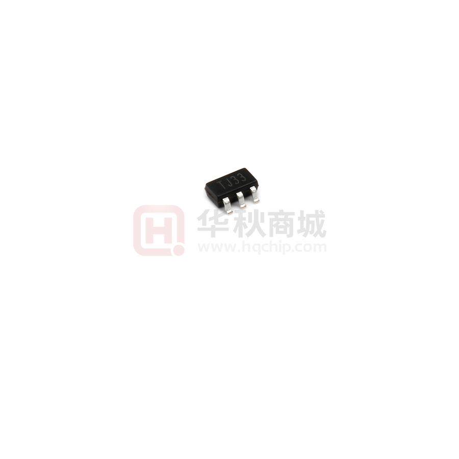
TJ33
Reel
Active
SOP-8PP
TJ5205DP-3.3
150mA, Enable, BYP
TJ5205-3.3
Reel
Contact us
SOT-23 5L
TJ5205SF5-3.6
150mA, Enable, BYP
TJ36
Reel
Active
SOP-8PP
TJ5205DP-3.6
150mA, Enable, BYP
TJ5205-3.6
Reel
Contact us
SOT-23 5L
TJ5205SF5-3.8
150mA, Enable, BYP
TJ38
Reel
Contact us
SOP-8PP
TJ5205DP-3.8
150mA, Enable, BYP
TJ5205-3.8
Reel
Contact us
SOT-23 5L
TJ5205SF5-4.0
150mA, Enable, BYP
TJ40
Reel
Contact us
SOP-8PP
TJ5205DP-4.0
150mA, Enable, BYP
TJ5205-4.0
Reel
Contact us
SOT-23 5L
TJ5205SF5-5.0
150mA, Enable, BYP
TJ50
Reel
Active
SOP-8PP
TJ5205DP-5.0
150mA, Enable, BYP
TJ5205-5.0
Reel
Contact us
Jan. 2016 - Rev. 1.8.3
-2-
HTC
�150mA Low Noise LDO Regulator
TJ5205
Ordering Information (Continued)
TJ
5205
Output Voltage : ADJ / 2.5V / 2.7V / 2.8V / 2.85V / 2.9V /
3.0V / 3.3V / 3.6V / 3.8V / 4.0V / 5.0V
Package Type
Root Name
SF5 : SOT-23-5L
DP : SOP-8PP
D : SOP-8
Product Code
PIN CONFIGURATION
VOUT
BYP/ADJ
5
4
1
2
VOUT
1
N.C
2
N.C
3
BYP/ADJ
4
3
VIN GND EN
SOT-23 5L
Thermal
PAD
8
VIN
7
GND
6
N.C
5
EN
SOP-8 / SOP-8PP
PIN DESCRIPTION
SOT-23
5LEAD
SOP-8/SOP-8PP 8 LEAD
Pin No.
Pin No.
Pin Name
Pin Function
1
VIN
Supply Input
2
GND
Pin Name
Pin Function
1
VOUT
Output Voltage
Ground
2/ 3/ 6
N.C
Not Connect
EN
Enable/Shutdown (Input):
CMOS compatible input.
Logic high=enable,
Logic low or open=shutdown
4
BYP / ADJ
Reference Bypass or
Output Adjust
4
BYP / ADJ
Reference Bypass or
Output Adjust
5
EN
Enable/Shutdown (Input):
CMOS compatible input.
Logic high=enable,
Logic low or open=shutdown
5
VOUT
Output Voltage
7
GND
Ground
-
-
-
8
VIN
Supply Input
3
Jan. 2016 - Rev. 1.8.3
-3-
HTC
�150mA Low Noise LDO Regulator
TJ5205
BLOCK DIAGRAM
[ Ultra-Low-Noise Fixed LDO Regulator ]
[ Ultra-Low-Noise Adjustable LDO Regulator ]
Jan. 2016 - Rev. 1.8.3
-4-
HTC
�150mA Low Noise LDO Regulator
TJ5205
TYPICAL APPLICATION
- Typical Fixed Output Application
VIN
VIN
VOUT
VOUT
TJ5205-X.X
EN
EN
GND
BYP
COUT=2.2uF
CBYP=470pF
(Optional)
- Typical Adjustable Output Application
VIN
VIN
VOUT
VOUT
TJ5205-X.X
EN
EN
GND
R1
BYP
COUT=2.2uF
CBYP=470pF
(Optional)
R2
* Note) BYP pin can be left open if low noise operation is not required.
VOUT = VREF(1+R2/R1)
VREF = 1.242V
VOUT(min) = 2.0V
Jan. 2016 - Rev. 1.8.3
-5-
HTC
�150mA Low Noise LDO Regulator
TJ5205
ELECTRICAL CHARACTERISTICS
VIN=VOUT+1V ; IL=100uA ; CL=1.0uF; VEN≥2.0V ; TJ=25°C, bold values indicate -40°C ≤ TJ ≤ +125°C; unless noted.
PARAMETER
Output Voltage Tolerance
SYMBOL
(Note 4)
VO
TEST CONDITION
Variation from specified VOUT
Adjustable Pin Voltage
(ADJ version)
VADJ
Output Voltage
Temp. Coefficient
ΔVO/ΔT
(Note 5)
Line Regulation
ΔVLINE
VIN = VOUT + 1V to 16V
Load Regulation
ΔVLOAD
IL = 0.1mA to 150mA
Dropout Voltage
(Note 7)
Quiescent Current
-1
-2
ppm/℃
%/V
0.02
0.2
0.5
%
IL = 100 uA
10
50
70
IL = 50 mA
110
150
230
IL = 100 mA
140
250
300
IL = 150 mA
165
275
350
VEN ≤ 0.4V (Shutdown)
VEN ≤ 0.18V (Shutdown)
0.01
1
5
(Note 6)
mV
120
350
uA
160
180
600
800
uA
IL = 100mA
600
1000
1500
IL = 150mA
1300
1900
2500
PSRR
frequency = 100Hz, IL = 100uA
75
Current Limit
ILIMIT
VOUT = 0V
320
(Note 9)
0.05
Jan. 2016 - Rev. 1.8.3
%
40
IGND
eno
1
2
V
Ripple Rejection
Output Noise
UNIT
0.012
0.05
IL = 50mA
Thermal Regulation
MAX.
1.242
VDROP
IQ
(Note 8)
TYP.
0.004
VEN ≥ 2.0V, IL = 100uA
Ground Pin Current
MIN.
IL=50mA, CL=2.2μ F, 470pF
from BYP to GND
-6-
260
dB
600
mA
%/W
nV
Hz
HTC
�150mA Low Noise LDO Regulator
TJ5205
Enable Input
PARAMETER
SYMBOL
TEST CONDITION
Enable Input Logic-Low Voltage
VIL
Regulator Shutdown
Enable Input Logic-High Voltage
VIH
Regulator enabled
IIL
VIL ≤ 0.4V
VIL ≤ 0.18V
IIH
VIH ≥ 2.0V
VIH ≥ 2.0V
Enable Input Current
Note 1.
Note 2.
Note 3.
Note 4.
Note 5.
Note 6.
Note 7.
Note 8.
Note 9.
MIN.
TYP.
MAX.
UNIT
0.4
0.18
V
2.0
2
V
0.01
-1
-2
uA
5
35
40
uA
Exceeding the absolute maximum rating may damage the device.
The device is not guaranteed to function outside its operating rating.
The maximum allowable power dissipation at any TA (ambient temperature) is PD(max)=(TJ(max)–TA)+ θJA. Exceeding the maximum
allowable power dissipation will result in excessive die temperature, and the regulator will go into thermal shutdown.
The TJ5205-ADJ has VREF=1.242V±1%, but minimum output voltage for TJ5205-ADJ must be above VOUTmin=2.0V.
Output voltage temperature coefficient is defined as the worst case voltage change divided by the total temperature range.
Regulation is measured at constant junction temperature using low duty cycle pulse testing. Parts are tested for load regulation in
the load range from 0.1mA to 150mA. Changes in output voltage due to heating effects are covered by the thermal regulation
specification.
Dropout Voltage is defined as the input to output differential at which the output voltage drops 2% below its nominal value measured
at 1V differential.
Ground pin current is the regulator quiescent current plus pass transistor base current. The total current drawn from the supply is
the sum of the load current plus the ground pin current.
Thermal regulation is defined as the change in output voltage at a time “t” after a change in power dissipation is applied, excluding
load or line regulation effects. Specifications are for a 150mA load pulse at VIN = 16V for t = 10ms.
Jan. 2016 - Rev. 1.8.3
-7-
HTC
�150mA Low Noise LDO Regulator
TJ5205
TYPICAL OPERATING CHARACTERISTICS
Jan. 2016 - Rev. 1.8.3
-8-
HTC
�150mA Low Noise LDO Regulator
TJ5205
TYPICAL OPERATING CHARACTERISTICS (Continued)
Jan. 2016 - Rev. 1.8.3
-9-
HTC
�150mA Low Noise LDO Regulator
TJ5205
REVISION NOTICE
The description in this data sheet can be revised without any notice to describe its electrical characteristics
properly.
Jan. 2016 - Rev. 1.8.3
- 10 -
HTC
�