7-Digit Darlington Current Driver
ULN2003A/ ULN2004A
FEATURES
•
•
•
•
•
•
•
7 Darlington Arrays per Package
500 mA Rated Collector Current (Single Output)
Output voltage 50V
Output Clamp Diodes
Input Compatible with Various Types of Logic
Relay-Driver Applications
Input pins placed opposite to output pins to simplify
layout
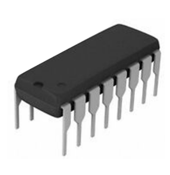
SOP-16
APPLICATION
•
•
•
•
•
•
Relay Drivers
Stepper and DC Brushed Motor Drivers
Lamp Drivers
Display Drivers
Line Drivers
Logic Buffers
DIP-16
ORDERING INFORMATION
Device
DESCRIPTION
Package
ULN2003AD
SOP-16
The ULN2003A and ULN2004A are monolithic highvoltage, high-current Darlington transistor arrays.
Each consists of seven NPN Darlington pairs that
feature high-voltage outputs with common-cathode
clamp diodes for switching inductive loads. The
collector-current rating of a single Darlington pair is 500
mA. The Darlington pairs may be paralleled for higher
current capability. Applications include relay drivers,
hammer drivers, lamp drivers, display drivers (LED and
gas discharge), line drivers, and logic buffers.
ULN2004AD
ULN2003AN
DIP-16
ULN2004AN
ABSOLUTE MAXIMUM RATINGS (Note 1)
CHARACTERISTIC
SYMBOL
MIN.
MAX.
UNIT
VO
-
50
V
VI
-
30
V
Peak Collector Current
IC
-
500
mA
Output Clamp Current
IOK
-
500
mA
Total Emitter-Terminal Current
IE
-
2.5
A
Maximum Junction Temperature
TJ
-
150
°C
Storage Temperature
TSTG
-60
150
°C
Lead Temperature (Soldering, 5sec)
TSOL
-
260
°C
Output Voltage
Input Voltage
(Note 2)
Apr. 2020 – Rev 1.1.1
1/8
HTC
�7-Digit Darlington Current Driver
ULN2003A/ ULN2004A
RECOMMENDED OPERATIONG CONDITIONS
CHARACTERISTIC
SYMBOL
MIN.
MAX.
UNIT
Output Voltage
VO
-
50
V
Junction Temperature
TJ
-40
125
°C
Operating Free-Air Temperature Range
TA
-40
85
°C
ƟJA-SOP-16
-
120
°C/W
ƟJA-DIP-16
-
80
°C/W
Package Thermal Resistance *
ORDERING INFORMATION
Package
Order No.
Description
Package Marking
Status
SOP-16
ULN2003AD
7-Digit Darlington Current Driver
ULN2003A
Active
SOP-16
ULN2004AD
7-Digit Darlington Current Driver
ULN2004A
Active
DIP-16
ULN2003AN
7-Digit Darlington Current Driver
ULN2003A
Active
DIP-16
ULN2004AN
7-Digit Darlington Current Driver
ULN2004A
Active
Apr. 2020 – Rev 1.1.1
2/8
HTC
�7-Digit Darlington Current Driver
ULN2003A/ ULN2004A
PIN CONFIGURATION
SOP-16 / DIP-16
PIN DESCRIPTION
Pin No.
Pin Name
SOP-16
DIP-16
1
1
1B
2
2
2B
3
3
3B
4
4
4B
5
5
5B
6
6
6B
7
7
7B
8
8
E
9
9
COM
10
10
7C
11
11
6C
12
12
5C
13
13
4C
14
14
3C
15
15
2C
16
16
1C
Apr. 2020 – Rev 1.1.1
Pin Function
Channel 1 through 7 Darlington Base Input
Common Emitter shared by All Channels
Common Cathode Node for Flyback Diodes
Channel 1 through 7 Darlington Collector Output
3/8
HTC
�7-Digit Darlington Current Driver
ULN2003A/ ULN2004A
PIN CONNECTION DIAGRAM
BLOCK DIAGRAM
D2
Input
B
R1
VT1
VT2
R2
R3
D3
E
D1
Apr. 2020 – Rev 1.1.1
COM
Output
C
4/8
R1 : Resistor
2.7kΩ for ULN2003A
10.5kΩ for ULN2004A
R2 : Resistor
7.2 kΩ
R3 : Resistor
3.0 kΩ
HTC
�7-Digit Darlington Current Driver
ULN2003A/ ULN2004A
ELECTRICAL CHARACTERISTICS (Note 3)
Limits in standard typeface are for TJ=25°C, unless otherwise specified.
PARAMETER
SYMBOL
TEST
FIGURE
TEST CONDITION
MIN.
TYP.
MAX.
IC=200mA
-
-
2.4
IC=250mA
-
-
2.7
IC=300mA
-
-
3.0
IC=125mA
-
-
5.0
IC=200mA
-
-
6.0
IC=275mA
-
-
7.0
IC=350mA
-
-
8.0
II=250µA, IC=100mA
-
0.9
1.1
II=350µA, IC=200mA
-
1.0
1.3
II=500µA, IC=350mA
-
1.2
1.6
VCE=50V,
II=0mA
-
-
50
II=0mA
-
-
100
VI=1V
-
-
500
-
1.7
2
V
50
65
-
µA
VI=3.85V
-
-
1.35
VI=5V
-
-
0.5
VI=12V
-
-
1.45
VR=50V
-
-
50
VR=50V, TA=85°C
-
-
100
VCE=2V,
for ULN2003A
ON-State Input Voltage
VI(ON)
Fig.1.
VCE=2V,
for ULN2004A
Collector-Emitter
Saturation Voltage
Output Leakage Current
VCE(SAT)
ICEX
Fig. 2.
Fig. 3.
Fig. 4.
VCE=50V,
TA=85°C
Clamp Forward Voltage
VF
Fig. 5.
IF=350mA
Off-State Input Current
II(OFF)
Fig. 6.
VCE=50V, IC=500µA, TA=85°C
for ULN2003A
Input Current
II(ON)
Fig. 7.
UNIT
V
V
µA
mA
for ULN2004A
Clamp Diode
Leakage Current
Turn-On Propagation
Delay Time
Turn-Off Propagation
Delay Time
IR
Fig. 8.
µA
tPLH
-
0.5VI to 0.5VO
-
0.25
1
tPHL
-
0.5VI to 0.5VO
-
0.25
1
µs
Note 1. Stresses beyond those listed under Absolute Maximum Ratings may cause permanent damage to the device. These
are stress ratings only, and functional operation of the device at these or any other conditions beyond those indicated
under Recommended Operating Conditions is not implied. Exposure to absolute-maximum-rated conditions for
extended periods may affect device reliability.
Note 2. All voltage values are with respect to the emitter/substrate terminal E, unless otherwise noted.
Note 3. The device is not guaranteed to function outside its operating ratings.
Apr. 2020 – Rev 1.1.1
5/8
HTC
�7-Digit Darlington Current Driver
ULN2003A/ ULN2004A
PARAMETER MEASUREMENT INFORMATION
Fig. 1. ON-State Input Voltage Test Circuit
Fig. 2. Collector-Emitter Saturation Voltage Test Circuit
Fig. 3. Output Leakage Current Test Circuit
Fig. 4. Output Leakage Current Test Circuit
Fig. 5. Clamp Forward Voltage Test Circuit
Fig. 6. Off-State Input Current Test Circuit
Fig. 7. Input Current Test Circuit
Fig. 8. Clamp Diode Leakage Current Test Circuit
Apr. 2020 – Rev 1.1.1
6/8
HTC
�7-Digit Darlington Current Driver
ULN2003A/ ULN2004A
Fig. 9. Propagation Delay Time Waveform
APPLICATION INFORMATION
T.B.D.
TYPICAL OPERATING CHARACTERISTICS
T.B.D.
Apr. 2020 – Rev 1.1.1
7/8
HTC
�7-Digit Darlington Current Driver
ULN2003A/ ULN2004A
REVISION NOTICE
The description in this data sheet is subject to change without any notice to describe its electrical characteristics
properly.
Apr. 2020 – Rev 1.1.1
8/8
HTC
�
很抱歉,暂时无法提供与“ULN2004AN”相匹配的价格&库存,您可以联系我们找货
免费人工找货