Automotive Grade Thin Film Chip Resistor
Type CPF-A Series
Key Features
AEC-Q200
Compliance
Advanced thin
film technology
RoHS compliant
Special
materials,
design, and
processing for
high sulfur
applications
Test proven
immunity to
humidity,
moisture, and
sulfur
TE Connectivity are pleased to introduce the sister of our CPF thin film chip
resistor, the AEC-Q200 compliant CPF-A series. Supplied on tape and reel for
ease of insertion, and available in 7 sizes / power ratings up to 0.5W
Characteristics – Electrical
Applications
Automotive
Size
Power
Rating
@70°C
Operating
Temp. Range
Max.
Operating
Voltage
Max.
Overload
Voltage
25V
50V
Resistance Range
±0.05%
±0.1%
±0.5% ±1%
Medical
0402 0.0625W -55 ~ +155°C
Testing /
Measurement
0603 0.0625W -55 ~ +155°C
50V
100V
0805
0.1W
-55 ~ +155°C
100V
200V
1206
0.125W
-55 ~ +155°C
150V
300V
1210
0.25W
-55 ~ +155°C
150V
300V
2010
0.25W
-55 ~ +155°C
150V
300V
2512
0.5W
-55 ~ +155°C
150V
300V
Communication
9.9Ω KΩ
Ω9.9KΩ
ΩKΩ
ΩKΩ
Ω99KΩ
Ω99KΩ
Ω99KΩ
9.9Ω -
KΩ
TCR
PPM/°C
±25
±50
Ω-
KΩ
Ω – MΩ
Ω - MΩ
Ω - MΩ
Ω - MΩ
Ω - MΩ
±25
±50
±25
±50
±25
±
±25
±50
±25
±50
±25
±50
Operating Voltage=√(P*R) or Max. operating voltage listed above, whichever is lower.
Overload Voltage=2.5*√(P*R) or Max. overload voltage listed above, whichever is lower
1773200-1 Rev. B 07/2018
Dimensions in
millimetres unless
otherwise specified
Dimensions Shown for
reference purposes only.
Specifications subject to
change
For Email, phone or live chat,
go to: www.te.com/help
�Automotive Grade Thin Film Chip Resistor
Derating Curve
Power ratio(%)
100
80
60
40
20
0
0
20
40
60
80
100
120
140
160
180
Ambient Temperature(℃)
Construction and dimensions
L
D1
W
T
D2
Alumina Substrate
Edge Electrode (NiCr) Resistor Layer (NiCr)
Bottom Electrode (Ag)
Barrier Layer (Ni)
Overcoat (Epoxy)
Top Electrode ( Ag-Pd or Cu) External Electrode (Sn) Marking
Weight
L
Size
W
T
D1
D2
(g)
(1000pcs)
1773200-1 Rev. B 07/2018
0402
1.00±0.05
0.50±0.05
0.30±0.05
0.20±0.10
0.20±0.10
0.54
0603
1.55±0.10
0.80±0.10
0.45±0.10
0.30±0.20
0.30±0.20
1.83
0805
2.00±0.15
1.25±0.15
0.55±0.10
0.30±0.20
0.40±0.20
4.71
1206
3.05±0.15
1.55±0.15
0.55±0.10
0.42±0.20
0.35±0.25
9.02
1210
3.10±0.15
2.40±0.15
0.55±0.10
0.40±0.20
0.55±0.25
10
2010
4.90±0.15
2.40±0.15
0.55±0.10
0.60±0.30
0.50±0.25
23.61
2512
6.30±0.15
3.10±0.15
0.55±0.10
0.60±0.30
0.50±0.25
38.06
Dimensions in
millimetres unless
otherwise specified
Dimensions Shown for
reference purposes only.
Specifications subject to
change
For Email, phone or live chat,
go to: www.te.com/help
�Automotive Grade Thin Film Chip Resistor
Environmental Characteristics
Item
Temperature Coefficient
of Resistance (TCR)
Requirement
As Spec
Short Term Overload
ΔR±0.05%
Insulation Resistance
>1000MΩ
Operational Life
ΔR±0.2%
Biased Humidity
ΔR±0.1%
High Temperature
Exposure
Temperature Cycling
Bending Strength (Board
Flex)
ΔR±0.2%
Solderability
95% min. coverage
Resistance to Soldering
Heat
ΔR±0.05%
Terminal Strength
Not Broken
Mechanical Shock
ΔR±0.1%
Vibration
ΔR±0.1%
ESD
ΔR±0.1%
Resistance to Solvents
Marking
undamaged
Sulfur Test
ΔR±1%
Flammability
No ignition of tissue
paper or scorching
of pinewood board
ΔR±0.1%
ΔR±0.1%
Test Method
JIS-C-5201-1 4.8
IEC-60115-1 4.8
-55°C~155°C, 25°C is the reference
temperature
JIS-C-5201-1 4.13
RCWV*2.5 or maximum overload
voltage, whichever is lower for 5
seconds
JIS-C-5201-1 4.6
IEC-60115-1 4.6
Apply 100vdc for 1 minute
MIL-STD-202 method 108
Condition D steady state TA=125°C at
rated power. Measurement taken 24±4
hours after test conclusion
MIL-STD-202 method 103
1000 hours 85°C 85%RH 10% of
operating power
MIL-STD-202 method 108
At 155°C for 1000 Hours
JESD-22 method JA- 104
JIS-C-5201-1 4.33
Bending once for 60 seconds
Bending displacement
2010 / 2512 = 2mm
Other sizes = 3mm
JIS-C-5201-1 4.17
IEC-60115-1 4.17
245 ±5°C for 3 seconds
JIS-C-5201-1 4.18
IEC-60115-1 4.18
260 ±5°C for 10 seconds
AEC-Q200-006
Force of 1.8kg for 60 seconds.
MIL-STD-202 method 213
Wave Form: Tolerance for half sine
shock pulse. Peak value
g’s. Nor al
duration (D) is 6
MIL-STD-202 method 204
5 g’s for
i utes. cycles each of
orientations.
10 ~ 2000 Hz
AEC-Q200-002
Human body 2KV
MIL-STD-202 method 215
Add aqueous wash chemical – OKEM
Clean or equivalent. Do not use banned
solvents.
EIA-997 (condition B)
105 ±2°C no power rating for 750 hours
UL94
V-0 or V-1 are acceptable. No electrical
testing required
RCWV (rated continuous working voltage)=√(P*R) or Max. operating voltage listed above,
whichever is lower
1773200-1 Rev. B 07/2018
Dimensions in
millimetres unless
otherwise specified
Dimensions Shown for
reference purposes only.
Specifications subject to
change
For Email, phone or live chat,
go to: www.te.com/help
�Automotive Grade Thin Film Chip Resistor
Marking:
0603 3digit marking for E96
14C
3digit marking for Example: 14C=13K7Ω 13C=13K3Ω
Marking Table
Code
E96
Code
E96
Code
E96
Code
E96
01
100
25
178
49
316
73
562
02
102
26
182
50
324
74
576
03
105
27
187
51
332
75
590
04
107
28
191
52
340
76
604
05
110
29
196
53
348
77
619
06
113
30
200
54
357
78
634
07
115
31
205
55
365
79
649
08
118
32
210
56
374
80
665
09
121
33
215
57
383
81
681
10
124
34
221
58
392
82
698
11
127
35
226
59
402
83
715
12
130
36
232
60
412
84
732
13
133
37
237
61
422
85
750
14
137
38
243
62
432
86
768
15
140
39
249
63
442
87
787
16
143
40
255
64
453
88
806
17
147
41
261
65
464
89
825
18
150
42
267
66
475
90
845
19
154
43
274
67
487
91
866
20
158
44
280
68
499
92
887
21
162
45
287
69
511
93
909
22
165
46
294
70
523
94
931
23
169
47
301
71
536
95
953
24
174
48
309
72
549
96
976
Code
A
B
C
D
E
F
G
H
X
Y
Z
Multiplier
100
101
102
103
104
105
106
107
10-1
10-2
10-3
0603 3digit marking for E24
E24
10
33
11
36
12
39
13
43
Example: 101=100Ω 102=1KΩ
15
47
16
51
18
56
20
62
22
68
24
75
27
92
30
91
0805~2512 4digit marking
Resistance
marking
1773200-1 Rev. B 07/2018
Ω
. KΩ
KΩ
1000
2201
1002
Dimensions in
millimetres unless
otherwise specified
9.9KΩ
4992
Dimensions Shown for
reference purposes only.
Specifications subject to
change
KΩ
1003
For Email, phone or live chat,
go to: www.te.com/help
�Automotive Grade Thin Film Chip Resistor
Packaging Quantity and reel specifications
Type
ØA
ØB
ØC
W
T
Emboss
Plastic
Paper
Tape (EA)
Tape (EA)
0402
178.0±1.0 60.0+1.0
13.5±0.7
9.5±1.0
11.5±1.0 1,000 / 5,000
-
0603
178.0±1.0 60.0+1.0
13.5±0.7
9.5±1.0
11.5±1.0 1,000 / 5,000
-
0805
178.0±1.0 60.0+1.0
13.5±0.7
9.5±1.0
11.5±1.0 1,000 / 5,000
-
1206
178.0±1.0 60.0+1.0
13.5±0.7
9.5±1.0
11.5±1.0 1,000 / 5,000
-
1210
178.0±1.0 60.0+1.0
13.5±0.7
9.5±1.0
11.5±1.0 1,000 / 5,000
2010
178.0±1.0 60.0+1.0
13.5±0.7
13.5±1.0
15.5±1.0
-
4,000
2512
178.0±1.0 60.0+1.0
13.5±0.7
13.5±1.0
15.5±1.0
-
4,000
Paper Tape Specifications
Type
A
B
0402 0.70±0.05 1.16±0.0
5
0603 1.10±0.05 1.90±0.0
5
0805 1.60±0.05 2.37±0.0
5
1206 2.00±0.05 3.55±0.0
5
1210 2.75±0.05 3.40±0.0
5
1773200-1 Rev. B 07/2018
W
E
F
P0
P1
P2
ΦD0
T
8.00±0.10 1.75±0.05 3.5±0.05 4.00±0.10 2.00±0.05 2.00±0.05 1.55±0.05 0.40±0.03
8.00±0.10 1.75±0.05 3.5±0.05 4.00±0.10 4.00±0.10 2.00±0.05 1.55±0.05 0.60±0.03
8.00±0.10 1.75±0.05 3.5±0.05 4.00±0.10 4.00±0.10 2.00±0.05 1.55±0.05 0.75±0.05
8.00±0.10 1.75±0.05 3.5±0.05 4.00±0.10 4.00±0.10 2.00±0.05 1.55±0.05 0.75±0.05
8.00±0.10 1.75±0.05 3.5±0.05 4.00±0.05 4.00±0.10 2.00±0.05 1.60±0.10 0.75±0.05
Dimensions in
millimetres unless
otherwise specified
Dimensions Shown for
reference purposes only.
Specifications subject to
change
For Email, phone or live chat,
go to: www.te.com/help
�Automotive Grade Thin Film Chip Resistor
Peel force of top cover tape
The peel speed shall be about 300mm/min±5%
The peel force of top cover tape shall be between 8gf to 60gf
Embossed Plastic Tape Specifications
Top Tape
ψ D0
E
A
F
B
W
ψ D1 1.4Min.
T
P1
Resistor
P2
P0
direction of unreeling
Emboss Tape
Type
A
B
W
E
F
P0
P1
P2
ØD0
T
2010 2.85±0.10 5.45±0.10 12.0±0.10 1.75±0.10 5.5±0.05 4.00±0.05 4.00±0.10 2.00±0.05 1.50+0.10 1.00±0.20
2512 3.40±0.10 6.65±0.10 12.0±0.10 1.75±0.10 5.5±0.05 4.00±0.05 4.00±0.10 2.00±0.05 1.50+0.10 1.00±0.20
Peel force of top cover tape
The peel speed shall be about 300mm/min±5%
The peel force of top cover tape shall be between 20gf to 80g
1773200-1 Rev. B 07/2018
Dimensions in
millimetres unless
otherwise specified
Dimensions Shown for
reference purposes only.
Specifications subject to
change
For Email, phone or live chat,
go to: www.te.com/help
�Automotive Grade Thin Film Chip Resistor
Recommended Land Pattern
C
B
A
Type
A
B
C
0402
0.50
0.50
0.60±0.2
0603
0.80
1.00
0.90±0.2
AR05
1.00
1.00
1.35±0.2
AR06
2.00
1.15
1.70±0.2
AR13
2.00
1.15
2.50±0.2
AR10
3.60
1.40
2.50±0.2
AR12
4.90
1.60
3.10±0.2
Solder Profile
IR Reflow Soldering
Time of IR reflow soldering at maximum temperature point 260°C:10s
1773200-1 Rev. B 07/2018
Dimensions in
millimetres unless
otherwise specified
Dimensions Shown for
reference purposes only.
Specifications subject to
change
For Email, phone or live chat,
go to: www.te.com/help
�Automotive Grade Thin Film Chip Resistor
Wave Soldering (Flow Soldering)
Time of wave soldering at maximum temperature point 260°C:10s
Hand Soldering
Time of soldering iron at maximum temperature point 410°C:5s
How To Order
1773200-1 Rev. B 07/2018
CPF-A
0805
B
1K0
E
1
Common
Part
CPF-A
Automotive
Grade
precision
chip resistor
Package Size
Tolerance
Value
TCR
B - ±0.1%
D - ±0.5%
F - ±1%
100R Ω
1K0 Ω
10K –
,
Ω
E - 25PPM
C - 50PPM
Packagin
g
1 – 1K
REEL
Blank –
5K REEL
0402
0603
0805
Dimensions in
millimetres unless
otherwise specified
1206
1210
2010
2512
Dimensions Shown for
reference purposes only.
Specifications subject to
change
For Email, phone or live chat,
go to: www.te.com/help
�
很抱歉,暂时无法提供与“CPF-A-0402B200RE”相匹配的价格&库存,您可以联系我们找货
免费人工找货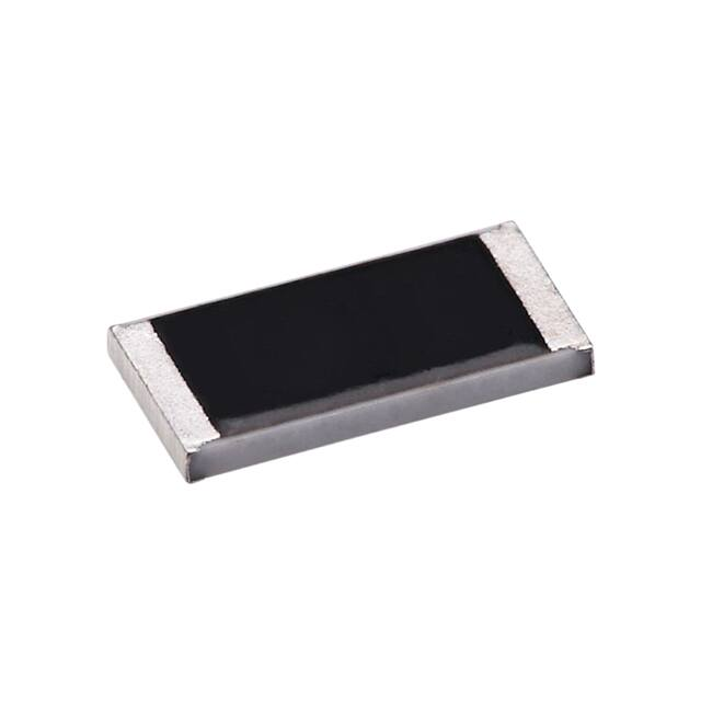


 工商网监
湘ICP备2023018690号
工商网监
湘ICP备2023018690号
