THICK FILM CHIP RESISTORS
Type CRG Series
Key Features
Thick Film
Resistors with
high power to
size ratio,
ideally suited
to industrial
and general
purpose use
Value range
from Ω to
MΩ
Eight package
sizes
Terminal finish
matte Sn over
Ni
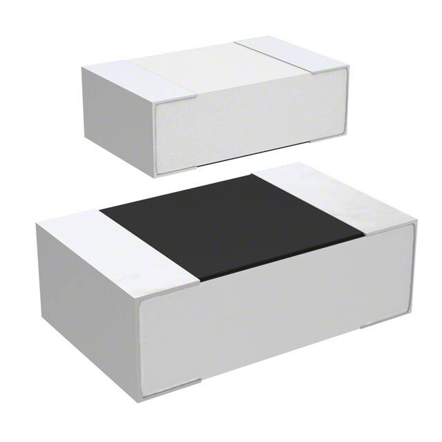
The resistive element is screen printed and fired, and a passivation layer added.
Each resistor is trimmed to tolerance by laser. The pre-scribed tile is then broken
into strips, the end plating fired on, and the strips broken into individual
components. Final termination finish is electroplated matte Sn over a Ni barrier
layer.
Electrical Characteristics
Type
0201
Power rating (W)
0.05
Resistance
Min
1R0
ra ge Ω
Max
10M
Tolerance (%)
1
Code Letter
F
Max Working Voltage
25V
Max Overload Voltage
50V
Dielectric Strength (V)
Rated current (Jumper) (A)0.5A
Max Overload Current (A)
1A
(Jumper)
Temperature Range
0402
0.0625
1R0
10M
1
F
50V
100V
100V
1A
0603
0.1
1R0
10M
1
F
75V
150V
300V
1A
0805
0.125
1R0
10M
1
F
150V
300V
500V
2A
1206
0.25
1R0
10M
1
F
200V
400V
500V
2A
1210
0.5
1R0
10M
1
F
200V
500V
500V
2A
2010
0.75W
1R0
10M
1
F
200V
500V
500V
2A
2512
1W
1R0
10M
1
F
200V
500V
500V
2A
2A
2A
5A
10A
10A
10A
10A
-55°C ~ 155°C
Power rating:
Resistors shall have a power rating based on continuous load operation at an ambient
temperature of 70 ℃ . For temperature in excess of 70 ℃ , The load shall be derate as
shown below
1773204 Rev J 12/2018
Dimensions in
millimetres unless
otherwise specified
Dimensions Shown for
reference purposes only.
Specifications subject to
change
For Email, phone or live chat,
go to: www.te.com/help
�THICK FILM CHIP RESISTORS
Derating Chart
Constuction
Dimensions:
Type
1773204 Rev J 12/2018
0201
0402
0603
L
0.60±0.03
1.00±0.10
1.60±0.10
0805
2.00±0.15
1206
3.10±0.15
1210
2010
2512
3.10±0.10
5.00±0.10
6.35±0.10
Dimensions in
millimetres unless
otherwise specified
W
0.30±0.03
0.50±0.05
0.80+0.15
-0.10
1.25+0.15
-0.10
1.55+0.15
-0.10
2.60±0.15
2.50±0.15
3.20±0.15
Dimensions (mm)
H
l1
0.23±0.03
0.10±0.05
0.35±0.05
0.20±0.10
0.45±0.10
0.30±0.20
l2
0.15±0.05
0.25±0.10
0.30±0.20
0.55±0.10
0.40±0.20
0.40±0.20
0.55±0.10
0.45±0.20
0.45±0.20
0.55±0.10
0.55±0.10
0.55±0.10
0.50±0.25
0.60±0.25
0.60±0.25
0.50±0.20
0.50±0.20
0.50±0.20
Dimensions Shown for
reference purposes only.
Specifications subject to
change
For Email, phone or live chat,
go to: www.te.com/help
�THICK FILM CHIP RESISTORS
Performance Specification:
Characteristic
*Insulation
Resistance
*Dielectric
Withstanding
Voltage
Temperature
Coefficient of
Resistance
(TCR)
Specification
,
MΩ Mi .
No evidence of flashover
mechanical damage, arcing
or insulation break down
Ω-
Ω:±
. Ω-
Ω:±
PPM/℃
Ω~
MΩ : ±
PPM/℃
For
:>
PPM/℃
Ω:±
Short Term
Overload
Resistance change rate is:
± % . % + . Ω Ma .
± % . % + . Ω Ma .
*Solderability
95 % coverage Min.
Soldering
Temp.
Reference
Electrical characteristics
shall be satisfied without
distinct deformation in
appearance.
(95 % coverage Min.)
Soldering
Heat
1773204 Rev J 12/2018
PPM/℃
Resistance change rate is:
± %+ . Ω Ma .
Dimensions in
millimetres unless
otherwise specified
Test Methods
(JIS C 5201-1)
Apply 500V DC between protective coating
and termination for 1 min, then measure
(Sub-clause 4.6)
Apply 100V(0402) 300V(0603) & 500V
(0805,1206,1210,2010,2512) AC between
protective coating and termination for 1
minute (Sub-clause 4.7)
Natural resistance change per temp.
degree centigrade.
R1: Resistance value at room temperature
(t1)
R2: Resistance value at room temp. plus
100 ℃ (t2)
(Sub-clause 4.8)
Permanent resistance change after the
application of a potential of 2.5 times
RCWV for 5 seconds
(Sub-clause 4.13)
Test temperature of solder : 245 ±3°C
Dipping time solder : 2-3 seconds
(Sub-clause 4.17)
Wave soldering condition: (2 cycles Max.)
Pre-heat : 100 ~ 120 ℃, 30 ± 5 sec.
Suggestion solder temp.: 235 ~ 255 ℃, 10
sec. (Max.)
Peak temp.: 260 ℃
Reflow soldering condition: (2 cycles
Max.)
Pre-heat : 150 ~ 180 ℃, 90 ~ 120 sec.
Suggestion solder temp.: 235 ~ 255 ℃, 20 ~
40 sec.
Peak temp.: 260 ℃
Hand soldering condition:
The soldering iron tip temperature should
be less than 300℃and maximum contract
time should be 5 sec.
Dip the resistor into a solder bath having a
temperature of 260°C±3°C and hold it for
10±1 seconds.
(Sub-clause 4.18)
Dimensions Shown for
reference purposes only.
Specifications subject to
change
For Email, phone or live chat,
go to: www.te.com/help
�THICK FILM CHIP RESISTORS
Performance Specification: (Continued)
Characteristic
Specification
Test Methods
(JIS C 5201-1)
Temperature Resistance change rate is
Resistance change after continuous
Cycling
5 cycles for duty cycle specified below :
± % . % + . Ω Max.
Step
Temperature Time
± % . % + . Ω Ma .
1
-55°C±3°C
30 mins
2
Room Temp
10~15 mins
3
155°C±2°C
30 mins
4
Room Temp
10~15 mins
(Sub-clause 4.19)
Load Life in
Resistance change rate is
Resistance change after 1,000 hours (1.5
Humidity
± % . % + . Ω Ma .
hours "on", 0.5 hour "off" ) at RCWV in a
± % . % + . Ω Ma .
humidity chamber controlled at 40℃ ± 2℃
and 90 to 95 % relative humidity
(Sub-clause 4.24.2.1)
Load Life
Resistance change rate is
Permanent resistance change after 1,000
± % . % + . Ω Ma .
hours operating at RCWV, with duty cycle
± % . % + . Ω Ma .
of (1.5 hours"on", 0.5 hour"off") at 70℃ ±
2℃ ambient
(Sub-clause 4.25.1)
Terminal
Resistance change rate is
Twist of Test Board :
Bending
± . % + . Ω Ma .
Y/X = 5/90 mm for 10 seconds
(Sub-clause 4.33)
The resistors of Ω o l a do the hara teristi oted of *
Environment Related Substance
This product complies to EU RoHS directive, EU PAHs directive, EU PFOS directive and
Halogen free. Ozone layer depleting substances are not used in our manufacturing
process of this product.
This product is not manufactured using Chloro fluorocarbons (CFCs),
Hydrochlorofluorocarbons (HCFCs), Hydrobromofluorocarbons (HBFCs) or other
ozone depleting substances in any phase of the manufacturing process.
Storage Condition
The performance of these products, including the solderability, is guaranteed for a
year from the date of arrival at your company, provided that they remain packed as
they were when delivered and stored at a temperature of 25°C ± 10°C and a relative
humidity of 60%RH ± 10%RH, chemical and dust free atmosphere
Even within the above guarantee periods, do not store these products in the
following conditions otherwise, their electrical performance and/or solderability may
be deteriorated, and the packaging materials (e.g. taping materials) may be deformed
or deteriorated, resulting in mounting failures.
1. In salty air or in air with a high concentration of corrosive gas, such as Cl2, H2S,
NH3, SO2, or NO2
2. In direct sunlight
1773204 Rev J 12/2018
Dimensions in
millimetres unless
otherwise specified
Dimensions Shown for
reference purposes only.
Specifications subject to
change
For Email, phone or live chat,
go to: www.te.com/help
�THICK FILM CHIP RESISTORS
Marking
E24 series 0603 – 2512 3 Digits – first two digits denote significant figures of
resistance and third digit denotes number of zeros thereafter. EG
222
=
2K2
Marking for E96 Series 0805 – 2512 4 digits – First three digits denote
significant figures of resistance and fourth digit denotes number of zeros
thereafter. EG.
1000
For ohmic alues elo
=
100R
R letter R de otes de i al poi t. EG
1R80
R8 / .8Ω
=
0201 and 0402 size chips are not marked
0603 E96 3 digit marking.
Resistance Code from table on next page, and Multiplier code from table
below
Multiplier Code
Code
Mult.
A
10⁰
B
10¹
C
10²
Coding
Formula
XX
E
10
F
10
Example
G
10
H
10
Dimensions in
millimetres unless
otherwise specified
Multiplier Code
X
10⁻¹
Y
10⁻²
Z
10⁻³
10K2
=
102
↓
02
X
10²
↓
C
=
02C
33R2
=
332
↓
51
X
⁻¹
↓
X
=
51X
X
Res. Code
1773204 Rev J 12/2018
D
10³
Dimensions Shown for
reference purposes only.
Specifications subject to
change
For Email, phone or live chat,
go to: www.te.com/help
�THICK FILM CHIP RESISTORS
Resistance Code
Label
Label shall be marked with the following item :
A. Nominal Resistance and Resistance Tolerance
B. Power Rating and Size
C. Quantity and description
D. Part No.
E. Lot No.
Ex.
1773204 Rev J 12/2018
Dimensions in
millimetres unless
otherwise specified
Dimensions Shown for
reference purposes only.
Specifications subject to
change
For Email, phone or live chat,
go to: www.te.com/help
�THICK FILM CHIP RESISTORS
Packing Specification:
Tape dimensions (mm)
A. Paper Taping
Type
A±0.2
B±0.2
C±0.05
ØD+0.1
-0
E±0.1
F±0.05
G±0.1
W±0.2
T±0.1
0201
0402
0.40
±0.05
0.65
0.70
±0.05
1.15
2.0
1.5
1.75
3.5
4.0
8.0
0.42
2.0
1.5
1.75
3.5
4.0
8.0
0.45
Type
A±0.2
B±0.2
C±0.05
E±0.1
F±0.05
G±0.1
W±0.2
T±0.1
1.90
2.40
3.60
3.50
2.0
2.0
2.0
2.0
ØD+0.1
-0
1.5
1.5
1.5
1.5
0603
0805
1206
1210
1.10
1.65
2.00
2.80
1.75
1.75
1.75
1.75
3.5
3.5
3.5
3.5
4.0
4.0
4.0
4.0
8.0
8.0
8.0
8.0
0.67
0.81
0.81
0.75
B. Embossed Taping
Type
2010
2512
A
±0.2
2.90
3.50
B
±0.2
5.60
6.70
C
±0.05
2.0
2.0
ØD+0.1
-0
1.5
1.5
ØD1+0.1
-0
1.5
1.5
E
±0.1
1.75
1.75
F
±0.05
5.5
5.5
G
±0.1
4.0
4.0
W
±0.2
12.0
12.0
T
±0.1
1.0
1.0
* Peeling Strength of Top Cover Tape
Test Condition: 0.1 to 0.7 N at a peel-off speed of 300 mm / min.
1773204 Rev J 12/2018
Dimensions in
millimetres unless
otherwise specified
Dimensions Shown for
reference purposes only.
Specifications subject to
change
For Email, phone or live chat,
go to: www.te.com/help
�THICK FILM CHIP RESISTORS
Reel Dimension (mm)
Type
Taping
0201
0402
0603
0805
1206
1210
2010
2512
Papar
Paper
Paper
Paper
Paper
Paper
Embossed
Embossed
Reel
Quantity
10,000
10,000
5,000
5,000
5,000
5,000
4,000
4,000
A ±0.5
B ±0.5
C ±0.5
D ±1
M ±1
W ±1
2
2
2
2
2
2
2
2
13
13
13
13
13
13
13
13
21
21
21
21
21
21
21
21
60
60
60
60
60
60
60
60
178
178
178
178
178
178
178
178
10
10
10
10
10
10
13.8
13.8
How To Order
CRG
Common Part
CRG - Thick Film
Chip Resistor
1773204 Rev J 12/2018
Dimensions in
millimetres unless
otherwise specified
0603
Size
0201
0402
0603
0805
1206
1210
2010
2512
F
Tolerance
10K
Resistance Value
oh
Ω R
K oh
Ω
K
F - ±1%
Dimensions Shown for
reference purposes only.
Specifications subject to
change
K oh
100K
M oh
Ω
Ω
M
For Email, phone or live chat,
go to: www.te.com/help
�