High Power Thick Film Chip Resistors
Type CRGH Series
Key Features
Thick Film
Resistors with
high power to
size ratio,
ideally suited
to industrial
and general
purpose use
Value range
from Ω to
MΩ
Seven package
sizes
Terminal finish
matte Sn over
Ni
The resistive element is screen printed and fired, and a passivation layer added.
Each resistor is trimmed to tolerance by laser. The pre-scribed tile is then broken
into strips, the end plating fired on, and the strips broken into individual
components. Final termination finish is electroplated matte Sn over a Ni barrier
layer.
Characteristics – Electrical
Size
0402
Power Rating
0.1
(W) @70°C
Resistance
1R0 ~ 10M
Range
Tolerance
Max. Working
50
Voltage (V)
Max. Overload
100
Voltage (V)
Dielectric
100
strength
Temperature
Range
1773204-1 Rev. F 02/2020
VersioDate
Dimensions in
millimetres unless
otherwise specified
0603
0805
1206
1210
2010
2512
0.2
0.33
0.5
0.75
1
2
R10 ~ 10M R10 ~ 10M R10 ~ 10M R10 ~ 10M R10 ~ 10M R10 ~ 10M
1% 5%
50
150
200
200
200
250
100
300
400
500
500
500
300
500
500
500
500
500
-55°C ~ 155°C
Dimensions Shown for
reference purposes only.
Specifications subject to
change
For Email, phone or live chat,
go to: www.te.com/help
�High Power Thick Film Chip Resistors
Power Rating:
Resistors shall have a power rating based on continuous load operation at an
ambient temperature of 70 ℃ . For temperature in excess of 70 ℃ , The load
shall be derated as shown below:
Voltage Rating
Resistors shall have a rated direct-current (DC) continuous working voltage or
an approximate sine-wave root-mean-square (RMS) alternating-current (AC)
continuous working voltage at commercial-line frequency and waveform
corresponding to the power rating, as determined from the following formula:
RCWV = √P x R
Where:
RCWV = Rated DC or RMS AC continuous working voltage at commercial-line
frequency and waveform (volt)
P = Power Rating (watt)
R = Nominal Resistance (ohm)
In no case shall the rated DC or RMS AC continuous working voltage be greater
than the applicable maximum value.
1773204-1 Rev. F 02/2020
VersioDate
Dimensions in
millimetres unless
otherwise specified
Dimensions Shown for
reference purposes only.
Specifications subject to
change
For Email, phone or live chat,
go to: www.te.com/help
�High Power Thick Film Chip Resistors
Construction:
Dimensions:
Type
1773204-1 Rev. F 02/2020
VersioDate
Dimensions (mm)
l1
W
H
0.50 ±0.05
0.35 ±0.05 0.20 ±0.10
CRGH0402
L
1.00 ±0.10
CRGH0603
1.60 ±0.10
0.80
CRGH0805
2.00 ±0.15
1.25
CRGH1206
3.10 ±0.15
1.55
CRGH1210
3.10 ±0.10
2.60
CRGH2010
CRGH2512
5.00 ±0.10
6.35 ±0.10
Dimensions in
millimetres unless
otherwise specified
±0.10
+0.15
-0.10
+0.15
-0.10
±0.20
2.50 ±0.20
3.20 ±0.20
l2
0.25 ±0.10
0.45 ±0.10
0.30 ±0.20
0.30 ±0.20
0.55 ±0.10
0.40 ±0.20
0.40 ±0.20
0.55 ±0.10
0.45 ±0.20
0.45 ±0.20
0.55 ±0.10
0.50 ±0.20
0.50 ±0.20
0.55 ±0.10
0.55 ±0.10
0.60 ±0.25
0.60 ±0.25
0.50 ±0.20
0.50 ±0.20
Dimensions Shown for
reference purposes only.
Specifications subject to
change
For Email, phone or live chat,
go to: www.te.com/help
�High Power Thick Film Chip Resistors
Performance Specification
Characteristic
Limits
Dielectric
Withstand
Voltage
No evidence of flashover
mechanical damage, arcing or
insulation break down
Temperature
Coefficient
. Ω≤R≤ .
Ω ±100
(CRGH0603 = ±200)
Ω ~ Ω: ±200PPM/℃
. Ω ~ MΩ: ±100PPM/℃
CRGH0402:
Ω ~ Ω: ±
PPM/℃
. Ω~
Ω: ±200PPM/℃
>
Ω: ±100PPM/℃
Short time
overload
Resistance change rate is
± % . % + . Ω Max.
± % . % + . Ω Max.
Solderability
95 % coverage Min.
Soldering
heat
Resistance change rate is:
± . %+ . Ω Max.
Temperature
cycling
Resistance change rate is
± % . % + . Ω Max.
± % . % + . Ω Max.
Humidity
Resistance change rate is
± % . % + . Ω Max.
± 1% (0.5% + . Ω Max.
Load life in
humidity
Resistance change rate is
± % . % + . Ω Max.
± % . % + . Ω Max.
1773204-1 Rev. F 02/2020
VersioDate
Dimensions in
millimetres unless
otherwise specified
Test Methods
( JIS C 5201-1 )
4.7 Clamped in the trough of a 90℃
metallic v-block and shall be tested at ac
potential respectively specified in the
type for 60-70 seconds
4.8 Natural resistance change per temp.
degree centigrade
R2 -R1
------------- x
PPM/°C
R1(t2-t1)
R1: Resistance value at room
temperature (T1)
R2: Resistance value at room temp. plus
100 ℃(T2)
Test pattern: room temp. (T1), room
temp. +100℃(T2)
4.13 Permanent resistance change after
the application of a potential of 2.5 times
RCWV for 5 seconds
Wave Solder:
Test temperature of solder: 245°C ±3°C
dipping time in solder : 2-3 seconds.
4.18 Dip the resistor into a solder bath
having a temperature of 260°C±3°C and
hold it for 10±1 seconds.
4.19 Resistance change after continuous
5 cycles for duty cycle specified below :
Step
Temperature Time
1
-55℃ ± 3℃
30 mins
10~15
2
Room temp.
mins
3
+155℃ ± 2℃
30 mins
10~15
4
Room temp.
mins
4.24 Temporary resistance change after
240 hours exposure in a humidity test
chamber controlled at 40±2°C and 9095% relative humidity
7.9 Resistance change after 1,000 hours
(1.5 hours "on", 0.5 hour "off" ) at RCWV
in a humidity chamber controlled at 40℃
± 2℃ and 90 to 95 % relative humidity
Dimensions Shown for
reference purposes only.
Specifications subject to
change
For Email, phone or live chat,
go to: www.te.com/help
�High Power Thick Film Chip Resistors
Performance Specification (continued)
Characteristic
Limits
Load Life
Resistance change rate is
± % . % + . Ω Max.
± % . % + . Ω Max.
Terminal
bending
Resistance change rate is
± . % + . Ω Max.
Test Methods
( JIS C 5201-1 )
4.25.1 Permanent resistance change after
1,000 hours operating at RCWV, with duty
cycle of (1.5 hours"on", 0.5 hour"off") at
70℃ ± 2℃ ambient
4.33 Twist of Test Board:
Y/X = 3/90 mm for 60 seconds
Marking
E24 series 0603 – 2512 3 Digits – first two digits denote significant figures of
resistance and third digit denotes number of zeros thereafter. EG
222
=
2K2
Marking for E96 Series 0805 – 2512 4 digits – First three digits denote
significant figures of resistance and fourth digit denotes number of zeros
thereafter. EG.
1000
For oh i
alues elo
=
100R
R letter R de otes decimal point. EG
1R80
R / . Ω
=
0402 size chips are not marked
0603 E96 3 digit marking.
Resistance Code from table on next page, and Multiplier code from table
below
Multiplier Code
Code
Mult.
A
10⁰
B
10¹
C
10²
Coding
Formula
XX
E
10
F
10
Example
G
10
H
10
Dimensions in
millimetres unless
otherwise specified
Multiplier Code
X
10⁻¹
Y
10⁻²
Z
10⁻³
10K2
=
102
↓
02
X
10²
↓
C
=
02C
33R2
=
332
↓
51
X
⁻¹
↓
X
=
51X
X
Res. Code
1773204-1 Rev. F 02/2020
VersioDate
D
10³
Dimensions Shown for
reference purposes only.
Specifications subject to
change
For Email, phone or live chat,
go to: www.te.com/help
�High Power Thick Film Chip Resistors
Resistance Code
Label
Label shall be marked with the following item :
A. Nominal Resistance and Resistance Tolerance
B. Power Rating and Size
C. Quantity and description
D. Part No.
E. Lot No.
Ex.
1773204-1 Rev. F 02/2020
VersioDate
Dimensions in
millimetres unless
otherwise specified
Dimensions Shown for
reference purposes only.
Specifications subject to
change
For Email, phone or live chat,
go to: www.te.com/help
�High Power Thick Film Chip Resistors
Packing Specification:
Tape dimensions (mm)
A. Paper Taping
Type
A±0.2
B±0.2
C±0.05
0402
0.65
1.15
2.0
Type
A±0.2
B±0.2
C±0.05
0603
0805
1206
1210
1.10
1.65
2.00
2.80
1.90
2.40
3.60
3.50
2.0
2.0
2.0
2.0
ØD+0.1
-0
1.5
E±0.1
F±0.05
G±0.1
W±0.2
T±0.1
1.75
3.5
4.0
8.0
0.45
ØD+0.1
-0
1.5
1.5
1.5
1.5
E±0.1
F±0.05
G±0.1
W±0.2
T±0.1
1.75
1.75
1.75
1.75
3.5
3.5
3.5
3.5
4.0
4.0
4.0
4.0
8.0
8.0
8.0
8.0
0.67
0.81
0.81
0.75
B. Embossed Taping
Type
2010
2512
A
±0.2
2.90
3.50
B
±0.2
5.60
6.70
C
±0.05
2.0
2.0
ØD+0.1
-0
1.5
1.5
ØD1+0.1
-0
1.5
1.5
E
±0.1
1.75
1.75
F
±0.05
5.5
5.5
G
±0.1
4.0
4.0
W
±0.2
12.0
12.0
T
±0.1
1.0
1.0
* Peeling Strength of Top Cover Tape
Test Condition: 0.1 to 0.7 N at a peel-off speed of 300 mm / min.
1773204-1 Rev. F 02/2020
VersioDate
Dimensions in
millimetres unless
otherwise specified
Dimensions Shown for
reference purposes only.
Specifications subject to
change
For Email, phone or live chat,
go to: www.te.com/help
�High Power Thick Film Chip Resistors
Reel Dimension (mm)
Type
Taping
0402
0603
0805
1206
1210
2010
2512
Paper
Paper
Paper
Paper
Paper
Embossed
Embossed
Reel
Quantity
10,000
5,000
5,000
5,000
5,000
4,000
4,000
A ±0.5
B ±0.5
C ±0.5
D ±1
M ±1
W ±1
2
2
2
2
2
2
2
13
13
13
13
13
13
13
21
21
21
21
21
21
21
60
60
60
60
60
60
60
178
178
178
178
178
178
178
10
10
10
10
10
13.8
13.8
How To Order
CRGH
Common Part
CRGH - High Power
Thick Film Chip
Resistor
1773204-1 Rev. F 02/2020
VersioDate
Dimensions in
millimetres unless
otherwise specified
0603
Size
0402
0603
0805
1206
1210
2010
2512
J
Tolerance
10K
Resistance Value
oh
Ω R
K oh
F - ±1%
J - ±5%
Dimensions Shown for
reference purposes only.
Specifications subject to
change
Ω
K
K oh
100K
M oh
Ω
Ω
M
For Email, phone or live chat,
go to: www.te.com/help
�
很抱歉,暂时无法提供与“CRGH2010J10R”相匹配的价格&库存,您可以联系我们找货
免费人工找货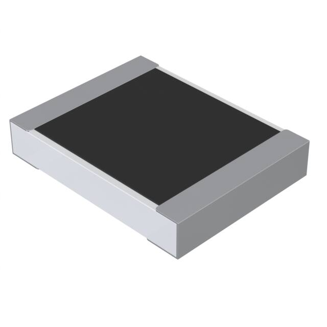


 工商网监
湘ICP备2023018690号
工商网监
湘ICP备2023018690号
