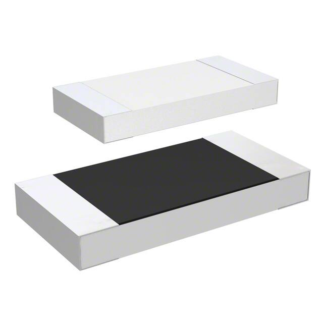
SMD Precision Pulse Thick Film Chip Resistor
Type CRGP Series
Key Features
Key Features
Small size and
light weight
Suitable for
both wave and
reflow
soldering
techniques
Supplied on
tape
Pulse Rated
7 different
package sizes
Terminal finish
matte Sn over
Ni
AEC-Q200
Compliant
TE Connectivity is pleased to introduce this SMD Pulse withstand thick film Chip
resistor, suitable for auto placement in volume and for most applications.
Available in five different packages and supplied on tape and reel for automatic
insertion processes. Standard values – E24 Series and now AEC-Q200 Qualified
Characteristics – Electrical
Type
Power Rating @ 70°C
Max. Working Voltage
Max. Overload Voltage
Dielectric Withstand
Temperature Range
Ambient Temperature
Type
Power Rating @ 70°C
Max. Working Voltage
Max. Overload Voltage
Dielectric Withstand
Temperature Range
Ambient Temperature
9-1773463-9 Rev. B 07/2021
Dimensions in
millimetres unless
otherwise specified
CRGP0402
0.125W
50V
100V
100V
CRGP1210
0.75W
200V
500V
500V
CRGP0603 CRGP0805
0.25W
0.33W
50V
150V
100V
300V
300V
500V
-55°C ~ +155°C
70°C
CRGP1206
0.5W
200V
400V
500V
CRGP2010
CRGP2512
1.25W
2W
400V
500V
800V
1000V
500V
500V
-55°C ~ +155°C
70°C
Dimensions Shown for
reference purposes only.
Specifications subject to
change
For Email, phone or live chat,
go to: www.te.com/help
�SMD Precision Pulse Thick Film Chip Resistor
Power derating curve
Power rating based on continuous load operation in ambient temperature of
70°C. For resistors operated in ambient temperatures above 70°C, power rating
must be derated in accordance with this curve.
Dimensions:
Type
CRGP0402
CRGP0603
CRGP0805
L
1.10±0.10
1.60±0.10
2.00±0.15
CRGP1206
3.10±0.15
CRGP1210
CRGP2010
CRGP2512
3.10±0.10
5.00±0.10
6.35±0.10
9-1773463-9 Rev. B 07/2021
Dimensions in
millimetres unless
otherwise specified
W
0.50±0.05
0.80±0.10
1.25+0.15
-0.10
1.55+0.15
-0.10
2.60±0.20
2.50±0.20
3.20±0.20
Dimension (mm)
H
ℓ
0.35±0.05
0.20±0.10
0.45±0.10
0.30±0.20
0.55±0.10
0.40±0.20
ℓ
0.25±0.10
0.30±0.20
0.40±0.20
0.55±0.10
0.45±0.20
0.45±0.20
0.55±0.10
0.55±0.10
0.55±0.10
0.55±0.25
0.60±0.25
0.60±0.25
0.50±0.20
0.50±0.20
0.50±0.20
Dimensions Shown for
reference purposes only.
Specifications subject to
change
For Email, phone or live chat,
go to: www.te.com/help
�SMD Precision Pulse Thick Film Chip Resistor
Construction:
Power Rating and Resistance Range:
Type
Power
Rating @
70°C
Tolerance
Resistance
Range
CRGP0402
0.125W
±1%
±5%
1R0 – 10M
CRGP0603
0.25W
±1%
±5%
1R0 – 10M
CRGP0805
0.33W
±1%
±5%
1R0 – 10M
0.5W
±1%
±5%
1R0 – 10M
CRGP1210
0.75W
±1%
±5%
1R0 – 10M
CRGP2010
1.25W
±1%
±5%
1R0 – 10M
CRGP2512
2W
±1%
±5%
1R0 – 10M
CRGP1206
Standard
Series
E24
E96 by
negotiation
E24
E96 by
negotiation
E24
E96 by
negotiation
E24
E96 by
negotiation
E24
E96 by
negotiation
E24
E96 by
negotiation
E24
E96 by
negotiation
Marking:
E24 series 0603 – 2512 3 Digits – first two digits denote significant figures of
resistance and third digit denotes number of zeros thereafter. EG
222
9-1773463-9 Rev. B 07/2021
Dimensions in
millimetres unless
otherwise specified
=
Dimensions Shown for
reference purposes only.
Specifications subject to
change
2K2
For Email, phone or live chat,
go to: www.te.com/help
�SMD Precision Pulse Thick Film Chip Resistor
Marking for E96 Series 0805 – 2512 4 digits – First three digits denote
significant figures of resistance and fourth digit denotes number of zeros
thereafter. EG.
1000
For ohmi
alues elo
=
100R
R letter R denotes decimal point. EG
1R80
=
R8 / .8Ω
0402 size chips are not marked
0603 E96 3 digit marking.
9-1773463-9 Rev. B 07/2021
Dimensions in
millimetres unless
otherwise specified
Dimensions Shown for
reference purposes only.
Specifications subject to
change
For Email, phone or live chat,
go to: www.te.com/help
�SMD Precision Pulse Thick Film Chip Resistor
Pulse withstand capacity
The single impulse graph is the result of 50 impulses of rectangular shape
applied at one-minute intervals. The limit of acceptance was a shift in
resistance of less than 1% from the initial value. The power applied was
subject to the restrictions of the maximum permissible impulse voltage
graph shown.
9-1773463-9 Rev. B 07/2021
Dimensions in
millimetres unless
otherwise specified
Dimensions Shown for
reference purposes only.
Specifications subject to
change
For Email, phone or live chat,
go to: www.te.com/help
�SMD Precision Pulse Thick Film Chip Resistor
Performance Specification:
Characteristic
Limits
Operational
life
±5%, ±10%, ±20%:
± %+ . Ω Max.
Temperature
Coefficient
Ω~ Ω : ±
PPM/°C
. Ω~ MΩ : ±
PPM/°C
External Visual
No Mechanical Damage
Physical
Dimensions
Reference 2.0 Dimension
Standards
Resistance to
Solvent
Marking Unsmeared
Terminal
Strength
Terminal
Bending
Not Broken
High
Temperature
Exposure
(Storage)
Temperature
Cycling
±(1%+0.1Ω)max
Solderability
95% coverage Min.
Soldering Heat
Resistance change rate is
± . %+ . Ω Max.
Insulation
Resistance
9-1773463-9 Rev. B 07/2021
±
. %± .
Ω Max.
Resistance change rate is
±5%, ±10%, ±20%: ±
. %+ . Ω Max.
,
MΩ or more
Dimensions in
millimetres unless
otherwise specified
Test Methods
(AEC-Q200)
125°C, at35% of operating power,
1000H(1.5 hours
“ON , . hour OFF . MIL-STD-202)
Natural resistance change per temp.
degree centigrade
R1-R2
--------- x ⁶ PPM/°C
R1(t2-t1)
R1 resistance value at room temperature
(t1)
R2 Resistance value at room temperature
+100°C (t2)
Electrical test not required. Inspect device
construction, marking and workmanship
(MIL-STD-883 Method 2009)
Verify physical dimensions to the
applicable device detail specification.
Note: User(s) and Suppliers spec. Electrical
test not required.
(JESD22 MH Method JB-100)
Note: Add Aqueous wash chemical – OKEM
Clean or equivalent.
Do not use banned solvents.
( MIL-STD-202 Method 215)
Force of 1.8kg for 60 seconds.
(JIS-C-6429)
Twist of Test Board :
Y/X = 5/90 mm for 10 seconds
(Sub-clause 4.33)
1000hrs. @T=155°C.Unpowered.
Measurement at 24±2 hours after test
conclusion. (MIL-STD-202 Method 108)
1000 Cycles (-55°C to +155°C).
Measurement at 24±2 hours after test
conclusion.
(JESD22 Method JA-104)
Test temperature of solder : 245 ± 3 ℃
Dwell time in solder : 2 ~ 3 seconds
(Sub-clause 4.17)
For both leaded & SMD. Electrical test not
required.
95% coverage Min. Magnification 50X.
Conditions:
( J-STD-002)
Dip the resistor into a solder bath having a
temperature of 260°C±3°C and hold it for
10±1 seconds
(Sub-clause 4.18)
Apply 500V DC between protective coating
and termination for 1 min, then measure
(Sub-clause 5.6)
Dimensions Shown for
reference purposes only.
Specifications subject to
change
For Email, phone or live chat,
go to: www.te.com/help
�SMD Precision Pulse Thick Film Chip Resistor
Characteristic
Limits
Test Methods
(AEC-Q200)
Solder Temp.
Reference
Electrical characteristics
shall be satisfied without
distinct deformation in
appearance.
(95% coverage Min.)
Wave soldering condition: (2 cycles Max.)
Pre-heat : 100 ~ 120 ℃, 30 ± 5 sec.
Suggestion solder temp.: 235 ~ 255 ℃, 10
seconds max.
Peak temp.: 260 ℃
Reflow soldering condition: (2 cycles Max.)
Pre-heat : 150 ~ 180 ℃, 90 ~ 120 sec.
Suggestion solder temp.: 235 ~ 255 ℃, 20 ~
40 sec.
Peak temp.: 260 ℃
Short term
overload
Resistance change rate is
± % : ± . % ± . Ω Max.
± % : ± . % ± . Ω Max.
Dielectric
Withstand
Voltage
No evidence of flashover,
mechanical damage,
arcing or insulation
breakdown.
Resistance change rate is:
± . % + . Ω Max.
Humidity
9-1773463-9 Rev. B 07/2021
Load Life In
Humidity
Resistance change rate is:
± % : ± . % ± . Ω Max.
± % : ± . % ± . Ω Max.
Load Life
Resistance change rate is:
± % : ± . % ± . Ω Max.
± % : ± . % ± . Ω Max.
Dimensions in
millimetres unless
otherwise specified
Hand Soldering 300°C 5 seconds
Permanent resistance change after the
application of a potential of 2.5 times
RCWV for 5 seconds
Sub-clause 4.13
Apply 500V AC between protective coating
and termination for 1 minute
(Sub-clause 4.7)
Temporary resistance change after 240
hours exposure in a humidity test chamber
controlled at 40±2°C and 90-95% relative
humidity
(Sub-clause 4.24)
Resistance change after 1,000 hours (1.5
hours "on", 0.5 hour "off") at RCWV in a
humidity chamber controlled at 40℃ ± 2℃
and 90 to 95 % relative humidity.
(Sub-clause 4.24.2.1)
Permanent resistance change after 1,000
hours operating at RCWV, with duty cycle
of (1.5 hours "on", 0.5 hour "off") at 70℃ ±
2℃ ambient
(Sub-clause 4.25.1
Dimensions Shown for
reference purposes only.
Specifications subject to
change
For Email, phone or live chat,
go to: www.te.com/help
�SMD Precision Pulse Thick Film Chip Resistor
Packaging Specification
Paper taping
Type
0402
0603
0805
1206
1210
A±
0.2
0.65
1.10
1.65
2.00
2.80
B±
0.2
1.15
1.90
2.40
3.60
3.50
C±
0.05
2.0
2.0
2.0
2.0
2.0
ØD +0.1
-0
1.5
1.5
1.5
1.5
1.5
E±
0.1
1.75
1.75
1.75
1.75
1.75
F±
0.05
3.5
3.5
3.5
3.5
3.5
G±
0.1
4.0
4.0
4.0
4.0
4.0
W±
0.2
8.0
8.0
8.0
8.0
8.0
T±
0.1
0.45
0.67
0.81
0.81
0.75
ØD1
+0.1
-0
1.5
1.5
E
±0.1
F
±0.05
G
±0.1
W
±0.2
T±
0.1
1.75
1.75
5.5
5.5
4.0
4.0
12.0
12.0
1.0
1.0
Embossed Taping
Type
A
±0.2
B
±0.2
C
±0.05
2010
2512
2.90
3.50
5.60
6.70
2.0
2.0
ØD
+0.1
-0
1.5
1.5
Peeling strength of cover tape:
Test condition: 0.1 to 0.7 N at a peel off speed of 300mm / min.
9-1773463-9 Rev. B 07/2021
Dimensions in
millimetres unless
otherwise specified
Dimensions Shown for
reference purposes only.
Specifications subject to
change
For Email, phone or live chat,
go to: www.te.com/help
�SMD Precision Pulse Thick Film Chip Resistor
Reel Dimensions (mm):
Type
Tape
0402
0603
0805
1206
1210
2010
2512
Paper
Paper
Paper
Paper
Paper
Embossed
Embossed
Reel
Qty
10,000
5,000
5,000
5,000
5,000
4,000
4,000
A ± 0.5
B ± 0.5
C ± 0.5
D±1
M±2
W±1
2
2
2
2
2
2
2
13
13
13
13
13
13
13
21
21
21
21
21
21
21
60
60
60
60
60
60
60
178
178
178
178
178
178
178
10
10
10
10
10
13.8
13.8
Environment Related Substance
This product complies to EU RoHS directive, EU PAHs directive, EU PFOS directive
and Halogen free.
Ozone layer depleting substances.
Ozone depleting substances are not used in our manufacturing process of this
product.
This product is not manufactured using Chloro fluorocarbons (CFCs),
Hydrochlorofluorocarbons (HCFCs), Hydrobromofluorocarbons (HBFCs) or other
ozone depleting substances in any phase of the manufacturing process.
Storage Condition
The performance of these products, including the solderability, is guaranteed for a
year from the date of arrival at your company, provided that they remain packed as
they were when delivered and stored at a temperature of 25°C ± 10°C and a relative
humidity of 60%RH ± 10%RH, chemical and dust free atmosphere
Even within the above guarantee periods, do not store these products in the
following conditions otherwise, their electrical performance and/or solderability
may be deteriorated, and the packaging materials (e.g. taping materials) may be
deformed or deteriorated, resulting in mounting failures.
1. In salty air or in air with a high concentration of corrosive gas, such as Cl2, H2S,
NH3, SO2, or NO2
2. In direct sunlight
9-1773463-9 Rev. B 07/2021
Dimensions in
millimetres unless
otherwise specified
Dimensions Shown for
reference purposes only.
Specifications subject to
change
For Email, phone or live chat,
go to: www.te.com/help
�SMD Precision Pulse Thick Film Chip Resistor
Solder Profile
Wave soldering condition: (2 cycles Max.)
Pre-heat : 100 ~ 120 ℃, 30 ± 5 sec.
Suggestion solder temp.: 235 ~ 255 ℃, 10 seconds
Peak temp.: 260 ℃
Reflow soldering condition: (2 cycles Max.)
Pre-heat : 150 ~ 180 ℃, 90 ~ 120 sec.
Suggestion solder temp.: 235 ~ 255 ℃, 20 ~ 40 seconds
Peak temp.: 260 ℃
Hand Soldering condition: The Soldering iron tip should be less than 300°C
and maximum contact time should be 5 seconds
How To Order
CRGP
Common Part
CRGP – Pulse
Withstand Thick
Film Chip Resistor
9-1773463-9 Rev. B 07/2021
Dimensions in
millimetres unless
otherwise specified
0603
Size
J
Tolerance
0402
0603
0805
1206
1210
2010
2512
F - ±1%
J - ±5%
10K
Resistance Value
ohm Ω R
K ohm
Dimensions Shown for
reference purposes only.
Specifications subject to
change
Ω 1K0
K ohm
100K
M ohm
Ω
Ω
M
For Email, phone or live chat,
go to: www.te.com/help
�


 工商网监
湘ICP备2023018690号
工商网监
湘ICP备2023018690号
