IDT74ALVCH162820
3.3V CMOS 10-BIT FLIP-FLOP WITH DUAL OUTPUTS
INDUSTRIAL TEMPERATURE RANGE
3.3V CMOS 10-BIT FLIPFLOP WITH DUAL OUTPUTS
IDT74ALVCH162820
FEATURES:
DESCRIPTION:
• 0.5 MICRON CMOS Technology
• Typical tSK(o) (Output Skew) < 250ps
• ESD > 2000V per MIL-STD-883, Method 3015; > 200V using
machine model (C = 200pF, R = 0)
• VCC = 3.3V ± 0.3V, Normal Range
• VCC = 2.7V to 3.6V, Extended Range
• VCC = 2.5V ± 0.2V
μ W typ. static)
• CMOS power levels (0.4μ
• Rail-to-Rail output swing for increased noise margin
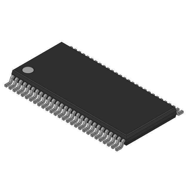
• Available in TSSOP package
This 10-bit flip-flop is built using advanced dual metal CMOS technology.
The ALVCH162820 is an edge-triggered D-type flip-flop. On the positive
transition of the clock (CLK) input, the device provides true data at the Q
outputs.
A buffered output-enable (OE) input can be used to place the ten outputs
in either a normal logic state (high or low logic level) or a high-impedance
state. In the high impedance state, the outputs neither load nor drive the bus
lines significantly. The high-impedance state and increased drive provide
the capability to drive bus lines without the need for interface or pullup
components. OE input does not affect the internal operation of the flip-flops.
Old data can be retained or new data can be entered while the outputs are
in the high-impedance state.
The ALVCH162820 has series resistors in the device output structure
which will significantly reduce line noise when used with light loads. This
driver has been designed to drive ±12mA at the designated threshold
levels.
The ALVCH162820 has “bus-hold” which retains the inputs’ last state
whenever the input goes to a high impedance. This prevents floating inputs
and eliminates the need for pull-up/down resistors.
DRIVE FEATURES:
• Balanced Output Drivers: ±12mA
• Low switching noise
APPLICATIONS:
• SDRAM Modules
• PC Motherboards
• Workstations
FUNCTIONAL BLOCK DIAGRAM
1OE
2OE
CLK
1
28
56
C1
D1
55
2
1Q1
3
1Q2
D1
TO NINE OTHER CHANNELS
The IDT logo is a registered trademark of Integrated Device Technology, Inc.
INDUSTRIAL TEMPERATURE RANGE
MAY 2006
1
© 2006 Integrated Device Technology, Inc.
DSC-4497/4
�IDT74ALVCH162820
3.3V CMOS 10-BIT FLIP-FLOP WITH DUAL OUTPUTS
INDUSTRIAL TEMPERATURE RANGE
ABSOLUTE MAXIMUM RATINGS(1)
PIN CONFIGURATION
Symbol
Description
VTERM(2)
Max
Unit
Terminal Voltage with Respect to GND
–0.5 to +4.6
V
1OE
1
56
CLK
VTERM(3)
Terminal Voltage with Respect to GND
–0.5 to VCC+0.5
V
1Q1
2
55
D1
TSTG
Storage Temperature
–65 to +150
°C
IOUT
DC Output Current
–50 to +50
mA
IIK
Continuous Clamp Current,
VI < 0 or VI > VCC
±50
mA
1Q2
3
54
NC
GND
4
53
GND
2Q1
5
52
D2
IOK
Continuous Clamp Current, VO < 0
–50
mA
2Q2
6
51
NC
ICC
ISS
Continuous Current through each
VCC or GND
±100
mA
VCC
7
50
VCC
3Q1
8
49
D3
3Q2
9
48
NC
4Q1
10
47
D4
GND
11
46
GND
4Q2
12
45
NC
5Q1
13
44
D5
5Q2
14
43
NC
6Q1
15
42
D6
6Q2
16
41
NC
7Q1
17
40
D7
GND
18
39
GND
7Q2
19
38
NC
20
37
D8
21
36
NC
8Q1
8Q2
NOTES:
1. Stresses greater than those listed under ABSOLUTE MAXIMUM RATINGS may cause
permanent damage to the device. This is a stress rating only and functional operation
of the device at these or any other conditions above those indicated in the operational
sections of this specification is not implied. Exposure to absolute maximum rating
conditions for extended periods may affect reliability.
2. VCC terminals.
3. All terminals except VCC.
CAPACITANCE (TA = +25°C, F = 1.0MHz)
Parameter(1)
Symbol
Conditions
Input Capacitance
VIN = 0V
5
7
pF
Output Capacitance
VOUT = 0V
7
9
pF
COUT
I/O Port Capacitance
VIN = 0V
7
9
pF
NOTE:
1. As applicable to the device type.
PIN DESCRIPTION
Pin Names
Description
(1)
Data Inputs
Clock Input
D9
xQx
3-State Outputs
33
NC
xOE
3-State Output Enable Inputs
25
32
GND
10Q1
26
31
D10
10Q2
27
30
NC
2OE
28
29
NC
9Q1
23
34
9Q2
24
GND
35
Unit
COUT
Dx
22
Max.
CIN
CLK
VCC
Typ.
VCC
NOTE:
1. These pins have "Bus-Hold". All other pins are standard inputs, outputs, or I/Os.
FUNCTION TABLE (EACH FLIP-FLOP)(1)
Inputs
TSSOP
TOP VIEW
Output
xOE
CLK
Dx
xQx
L
↑
H
H
L
↑
L
L
L
H or L
X
Q0(2)
H
X
X
Z
NOTES:
1. H = HIGH Voltage Level
L = LOW Voltage Level
X = Don’t Care
Z = High Impedance
↑ = LOW-to-HIGH transition
2. Output level before the indicated steady-state input conditions were established.
2
�IDT74ALVCH162820
3.3V CMOS 10-BIT FLIP-FLOP WITH DUAL OUTPUTS
INDUSTRIAL TEMPERATURE RANGE
DC ELECTRICAL CHARACTERISTICS OVER OPERATING RANGE
Following Conditions Apply Unless Otherwise Specified:
Operating Condition: TA = –40°C to +85°C
Symbol
VIH
VIL
Min.
Typ.(1)
Max.
Unit
VCC = 2.3V to 2.7V
1.7
—
—
V
VCC = 2.7V to 3.6V
2
—
—
VCC = 2.3V to 2.7V
—
—
0.7
VCC = 2.7V to 3.6V
—
—
0.8
Parameter
Input HIGH Voltage Level
Input LOW Voltage Level
Test Conditions
V
IIH
Input HIGH Current
VCC = 3.6V
VI = VCC
—
—
±5
µA
IIL
Input LOW Current
VCC = 3.6V
VI = GND
—
—
±5
µA
IOZH
High Impedance Output Current
VCC = 3.6V
VO = VCC
—
—
±10
µA
IOZL
(3-State Output pins)
VO = GND
—
—
±10
VIK
Clamp Diode Voltage
VCC = 2.3V, IIN = –18mA
—
–0.7
–1.2
V
VH
ICCL
ICCH
ICCZ
ΔICC
Input Hysteresis
Quiescent Power Supply Current
VCC = 3.3V
VCC = 3.6V
VIN = GND or VCC
—
—
100
0.1
—
40
mV
µA
Quiescent Power Supply Current
Variation
One input at VCC - 0.6V, other inputs at VCC or GND
—
—
750
µA
Min.
Typ.(2)
Max.
Unit
– 75
—
—
µA
VI = 0.8V
75
—
—
VI = 1.7V
– 45
—
—
NOTE:
1. Typical values are at VCC = 3.3V, +25°C ambient.
BUS-HOLD CHARACTERISTICS
Symbol
IBHH
Parameter(1)
Test Conditions
Bus-Hold Input Sustain Current
VCC = 3V
Bus-Hold Input Sustain Current
VCC = 2.3V
Bus-Hold Input Overdrive Current
VCC = 3.6V
VI = 2V
IBHL
IBHH
IBHL
IBHHO
IBHLO
NOTES:
1. Pins with Bus-Hold are identified in the pin description.
2. Typical values are at VCC = 3.3V, +25°C ambient.
3
VI = 0.7V
45
—
—
VI = 0 to 3.6V
—
—
±500
µA
µA
�IDT74ALVCH162820
3.3V CMOS 10-BIT FLIP-FLOP WITH DUAL OUTPUTS
INDUSTRIAL TEMPERATURE RANGE
OUTPUT DRIVE CHARACTERISTICS
Symbol
VOH
Test Conditions(1)
Parameter
Output HIGH Voltage
VCC = 2.3V to 3.6V
IOH = – 0.1mA
VCC = 2.3V
VCC = 2.7V
VCC = 3V
VOL
Output LOW Voltage
VCC = 2.3V to 3.6V
VCC = 2.3V
Min.
Max.
Unit
VCC – 0.2
—
V
IOH = – 4mA
1.9
—
IOH = – 6mA
1.7
—
IOH = – 4mA
2.2
—
IOH = – 8mA
2
—
IOH = – 6mA
2.4
—
IOH = – 12mA
2
—
IOL = 0.1mA
—
0.2
IOL = 4mA
—
0.4
IOL = 6mA
—
0.55
VCC = 2.7V
IOL = 4mA
—
0.4
IOL = 8mA
—
0.6
VCC = 3V
IOL = 6mA
—
0.55
IOL = 12mA
—
0.8
V
NOTE:
1. VIH and VIL must be within the min. or max. range shown in the DC ELECTRICAL CHARACTERISTICS OVER OPERATING RANGE table for the appropriate VCC range.
TA = – 40°C to + 85°C.
OPERATING CHARACTERISTICS, TA = 25°C
Symbol
Parameter
CPD
Power Dissipation Capacitance per Flip Flop Outputs enabled
CPD
Power Dissipation Capacitance per Flip Flop Outputs disabled
VCC = 2.5V ± 0.2V
VCC = 3.3V ± 0.3V
Test Conditions
Typical
Typical
Unit
CL = 0pF, f = 10Mhz
68
66
pF
39
47
SWITCHING CHARACTERISTICS(1)
VCC = 2.5V ± 0.2V
Symbol
Parameter
Min.
fMAX
tPLH
Propagation Delay
tPHL
CLK to xQx
tPZH
Output Enable Time
VCC = 2.7V
Max.
Min.
150
—
1
4.5
1
VCC = 3.3V ± 0.3V
Max.
Min.
Max.
Unit
150
—
—
4.5
150
—
MHz
1
4.3
ns
6.9
—
6.8
1
5.6
ns
1
6.2
—
5.5
1
5
ns
1.7
—
1.8
—
1.4
—
ns
tPZL
OE to xQx
tPHZ
Output Disable Time
tPLZ
OE to xQx
tSU
Set-up Time, HIGH or LOW, data before CLK↑
tH
Hold Time, HIGH or LOW, data after CLK↑
1.1
—
1.1
—
1
—
ns
tW
Pulse Width, CLK HIGH or LOW
3.3
—
3.3
—
3.3
—
ns
Output Skew(2)
—
—
—
—
—
500
ps
tSK(O)
NOTES:
1. See TEST CIRCUITS AND WAVEFORMS. TA = – 40°C to + 85°C.
2 Skew between any two outputs of the same package and switching in the same direction.
4
�IDT74ALVCH162820
3.3V CMOS 10-BIT FLIP-FLOP WITH DUAL OUTPUTS
INDUSTRIAL TEMPERATURE RANGE
TEST CIRCUITS AND WAVEFORMS
TEST CONDITIONS
VCC(1)= 3.3V±0.3V VCC(1)= 2.7V
Symbol
VCC(2)= 2.5V±0.2V
Unit
VLOAD
6
6
2 x Vcc
V
VIH
2.7
2.7
Vcc
V
VT
1.5
1.5
Vcc / 2
V
VLZ
300
300
150
mV
VHZ
300
300
150
mV
CL
50
50
30
pF
VIN
tPHL
VIH
VT
0V
Propagation Delay
DISABLE
ENABLE
CONTROL
INPUT
GND
tPZL
D.U.T.
OUTPUT
SWITCH
NORMALLY
CLOSED
LOW
tPZH
OUTPUT
SWITCH
NORMALLY
OPEN
HIGH
500Ω
RT
tPLH
ALVC Link
VOUT
Pulse
Generator
tPHL
OPPOSITE PHASE
INPUT TRANSITION
Open
500Ω
tPLH
OUTPUT
VLOAD
VCC
(1, 2)
VIH
VT
0V
VOH
VT
VOL
SAME PHASE
INPUT TRANSITION
CL
ALVC Link
Test Circuit for All Outputs
tPLZ
VLOAD/2
VT
VIH
VT
0V
VLOAD/2
VLZ
VOL
tPHZ
VOH
VHZ
0V
VT
0V
ALVC Link
DEFINITIONS:
CL = Load capacitance: includes jig and probe capacitance.
RT = Termination resistance: should be equal to ZOUT of the Pulse Generator.
Enable and Disable Times
NOTE:
1. Diagram shown for input Control Enable-LOW and input Control Disable-HIGH.
NOTES:
1. Pulse Generator for All Pulses: Rate ≤ 1.0MHz; tF ≤ 2.5ns; tR ≤ 2.5ns.
2. Pulse Generator for All Pulses: Rate ≤ 1.0MHz; tF ≤ 2ns; tR ≤ 2ns.
DATA
INPUT
SWITCH POSITION
Test
GND
All Other Tests
Open
INPUT
OUTPUT 1
tPLH1
SYNCHRONOUS
CONTROL
VIH
VT
0V
VOH
VT
VOL
tSK (x)
OUTPUT 2
LOW-HIGH-LOW
PULSE
VT
tW
HIGH-LOW-HIGH
PULSE
VT
ALVC Link
tPHL2
Pulse Width
tSK(x) = tPLH2 - tPLH1 or tPHL2 - tPHL1
Output Skew - tSK(X)
tH
Set-up, Hold, and Release Times
VOH
VT
VOL
tPLH2
tSU
ALVC Link
tPHL1
tSK (x)
tREM
ASYNCHRONOUS
CONTROL
VLOAD
Disable High
Enable High
tH
TIMING
INPUT
Switch
Open Drain
Disable Low
Enable Low
tSU
VIH
VT
0V
VIH
VT
0V
VIH
VT
0V
VIH
VT
0V
ALVC Link
NOTES:
1. For tSK(o) OUTPUT1 and OUTPUT2 are any two outputs.
2. For tSK(b) OUTPUT1 and OUTPUT2 are in the same bank.
5
�IDT74ALVCH162820
3.3V CMOS 10-BIT FLIP-FLOP WITH DUAL OUTPUTS
INDUSTRIAL TEMPERATURE RANGE
ORDERING INFORMATION
IDT
ALVC X
XX
Bus-Hold
Temp. Range
XX
Family
XX
XXX
Device Type Package
CORPORATE HEADQUARTERS
6024 Silver Creek Valley Road
San Jose, CA 95138
PA
PAG
Thin Shrink Small Outline Package
TSSOP - Green
820
10-Bit Flip Flop with Dual Outputs, 3-State Outputs
162
Double-Density with Resistors, ±12mA
H
Bus-Hold
74
–40°C to +85°C
for SALES:
800-345-7015 or 408-284-8200
fax: 408-284-2775
www.idt.com
6
for Tech Support:
logichelp@idt.com
�
很抱歉,暂时无法提供与“74ALVCH162820PAG”相匹配的价格&库存,您可以联系我们找货
免费人工找货