Automotive Sensor Signal
Conditioner with Dual Analog Output
Brief Description
Benefits
The ZSSC3154 is an integrated circuit for highly
accurate amplification and sensor-specific correction
of a bridge sensor signal. Up to two temperature
sensors can also be read in parallel.
•
•
The circuitry provides different configurations of the
analog outputs to show two measurement results
simultaneously. This also allows generating a complementary bridge sensor signal, which is often a
requirement in safety-relevant applications.
•
•
The ZSSC3154 can measure and process two external temperature sensors to compensate the temperature drift of the bridge sensor signal and to output a
separate temperature signal.
•
An integrated calibration microcontroller with an onchip EEPROM performs the digital compensation of
the sensor offset, the sensitivity, the temperature
drift, and the nonlinearity of a sensor signal.
•
•
•
•
•
•
•
•
Evaluation Kit
Application Notes
Calculation Tools
•
•
Differential bridge sensor input
Half-bridge sensor or temperature sensor input
Digital compensation of offset, gain, nonlinearity,
and temperature dependency
Two analog outputs; behavior programmable by
EEPROM configuration
Sequential analog output mode provides two
measurement values at one output pin
On-chip diagnostic and safety features including
sensor connection diagnostic and broken-chip
detection
2 EEPROM words for arbitrary user data
Multiple configurable output options
•
•
•
•
•
Supply voltage: 4.5 to 5.5V
Maximum supply voltage: 7.7V
Input span: 1.8 to 267mV/V
ADC resolution: 14 bit
Output resolution: > 12 bit from 10% to 90%
Operating temperature range: -40°C to 150°C
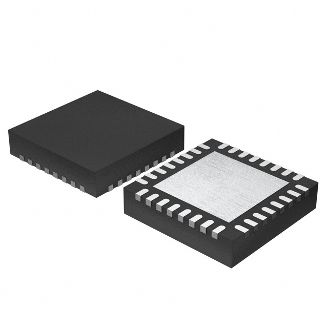
Package: QFN32 (5x5mm; wettable flank) or die
ZSSC3154 Basic Circuit
DFBH
VDDA
VTN2
VSSA
VTN1
SDA
VBR_T
VBP
VBR_B
VBN
© 2016 Integrated Device Technology, Inc.
1
ZSSC3154
•
Bridge sensor signal validation for safety
applications via two antivalent analog outputs or
via half-bridge sensor measurement output
Simultaneous measurement of sensor signals,
including temperature signal for compensation
and for temperature output
Efficient use of non-calibrated elements for
bridge sensors and temperature sensors without
external trimming components
Single-pass end-of-line calibration algorithm
minimizes production costs
Excellent EMC/ESD robustness and AEC-Q100
qualification
Physical Characteristics
Features
•
Datasheet
Available Support
The single-pass, digital end-of-line calibration combined with the integrated broken-chip detection supports automatic and highly efficient mass production.
•
ZSSC3154
SCL
VDD
VDDE
VCC
AOUT1
AOUT1
AOUT2
AOUT2
VSSE
GND
January 22, 2016
�ZSSC3154
Automotive Sensor Signal
Conditioner with Dual Analog Output
Datasheet
ZSSC3154 Block Diagram
External
Temperature
Sensor 2
External
Temperature
Sensor 1
Conditioning Coefficients
Temperature
Sensor Select
Gain
Factor
Offset
Shift
ADC
Mode
EEPROM
I2C™*
I2C™*
Diagnostic Fault
Band Mode
RAM
AOUT2
BAMP
MUX
PGA
ADC
CMC
DAC
AOUT1
OWI
(Digital
Data IO)
BAMP
Analog Front-End AFE
Sensor
Bridge
ROM
Internal
Temperature
Sensor
ZACwire™
Conditioning Calculation
Conditioning Formula
Digital Core
Interfaces
* I2C™ is a trademark of NXP.
Ordering Information
Product Sales Code
Description
Package
ZSSC3154BA1B
ZSSC3154 Die – Temperature Range -40 to 125°C
Wafer
ZSSC3154BA1C
ZSSC3154 Die – Temperature Range -40 to 125°C
Sawn on frame
ZSSC3154BA3R
ZSSC3154 QFN32 (5x5 mm; wettable flank) – Temperature Range -40 to 125 °C
Reel
ZSSC3154BE3R
ZSSC3154 QFN32 (5x5 mm; wettable flank) – Temperature Range -40 to 150 °C
Reel
ZSSC3154KIT
ZSSC3154 SSC Evaluation Kit: Communication Board, SSC Board, Sensor
Replacement Board, 5 QFN32 samples (software can be downloaded from the
product page www.IDT.com/ZSSC3154)
Kit
© 2016 Integrated Device Technology, Inc.
2
January 22, 2016
�ZSSC3154 Datasheet
Contents
1
Electrical Characteristics .................................................................................................................................. 5
1.1
Absolute Maximum Ratings ....................................................................................................................... 5
1.2
Operating Conditions ................................................................................................................................. 5
1.3
Electrical Parameters ................................................................................................................................ 6
1.3.1
Supply Current and System Operation Conditions ............................................................................. 6
1.3.2
Analog Front-End Characteristics ....................................................................................................... 6
1.3.3
Temperature Measurement ................................................................................................................ 7
1.3.4
Sensor Diagnostic Tasks .................................................................................................................... 7
1.3.5
A/D Conversion ................................................................................................................................... 8
1.3.6
D/A Conversion and Analog Outputs (Pins AOUT1 and AOUT2) ...................................................... 8
1.3.7
System Response ............................................................................................................................... 9
1.4
Interface Characteristics and EEPROM .................................................................................................. 10
TM
1.4.1
I2C Interface .................................................................................................................................. 10
TM
1.4.2
ZACwire One Wire Interface .......................................................................................................... 10
1.4.3
EEPROM ........................................................................................................................................... 10
2 Circuit Description .......................................................................................................................................... 11
2.1
Signal Flow .............................................................................................................................................. 11
2.2
Application Modes ................................................................................................................................... 12
2.3
System Control ........................................................................................................................................ 13
2.3.1
Main System Tasks ........................................................................................................................... 13
2.3.2
General Working Modes ................................................................................................................... 13
2.4
Normal Operation Mode .......................................................................................................................... 13
2.4.1
Startup Phase ................................................................................................................................... 13
2.4.2
Measurement Cycle .......................................................................................................................... 14
2.4.3
Conditioning Calculation ................................................................................................................... 14
2.5
Bridge Sensor Measurement ................................................................................................................... 15
2.6
Temperature Measurement ..................................................................................................................... 15
2.7
Half-Bridge Sensor Measurement ........................................................................................................... 15
2.8
Analog Front End ..................................................................................................................................... 16
2.8.1
Programmable Gain Amplifier ........................................................................................................... 16
2.8.2
Offset Compensation ........................................................................................................................ 17
2.8.3
Analog-to-Digital Converter ............................................................................................................... 18
2.9
Signal Outputs ......................................................................................................................................... 18
2.9.1
Analog Output ................................................................................................................................... 18
2.9.2
Sequential Analog Output ................................................................................................................. 19
2.9.3
Digital Output .................................................................................................................................... 19
2.10 Serial Digital Interfaces ............................................................................................................................ 19
2.11 Failsafe Features ..................................................................................................................................... 20
© 2016 Integrated Device Technology, Inc.
3
January 22, 2016
�ZSSC3154 Datasheet
2.12 Overvoltage and Short Circuit Protection ................................................................................................ 20
3 Application Circuits and External Components .............................................................................................. 21
3.1
Application Circuit Examples ................................................................................................................... 21
3.2
External Components .............................................................................................................................. 22
4 ESD Protection and EMC Specification ......................................................................................................... 22
5 Pin Configuration and Package ...................................................................................................................... 23
6 Reliability and RoHS Conformity .................................................................................................................... 25
7 Ordering Information ...................................................................................................................................... 25
8 Related Documents ........................................................................................................................................ 25
9 Glossary ......................................................................................................................................................... 26
10 Document Revision History ............................................................................................................................ 27
List of Figures
Figure 2.1
Figure 2.2
Figure 2.3
Figure 3.1
Figure 3.2
Figure 5.1
Block Diagram of the ZSSC3154 ...................................................................................................... 11
Example of Measurement Cycle with Bridge Sensor Signal and Temperature Measurement ........ 14
Sequential Analog Output—Example Sequence if the DFBH Pin is Unconnected .......................... 19
Application Circuit with Two Analog Outputs and Diagnostic Fault Band Level Low ....................... 21
Application Circuit with Two Analog Outputs and Diagnostic Fault Band Level High ...................... 21
Pin Map and Pad Position of the ZSSC3154 .................................................................................... 24
List of Tables
Table 1.1
Table 1.2
Table 1.3
Table 1.4
Table 2.1
Table 2.2
Table 2.3
Table 3.1
Table 5.1
Absolute Maximum Ratings ................................................................................................................ 5
Operating Conditions .......................................................................................................................... 5
Electrical Parameters .......................................................................................................................... 6
Interface Characteristics and EEPROM ........................................................................................... 10
Adjustable Gains and Resulting Sensor Signal Spans and Common Mode Ranges ...................... 16
Extended Analog Offset Compensation Ranges (XZC) ................................................................... 17
ADC Resolution versus Output Resolution and Sample Rate .......................................................... 18
Dimensioning of External Components for the Application Examples ............................................. 22
Pin Configuration .............................................................................................................................. 23
© 2016 Integrated Device Technology, Inc.
4
January 22, 2016
�ZSSC3154 Datasheet
1
Electrical Characteristics
1.1 Absolute Maximum Ratings
The absolute maximum ratings are stress ratings only. The ZSSC3154 might not function or be operable above
the recommended operating conditions. Stresses exceeding the absolute maximum ratings might also damage
the device. In addition, extended exposure to stresses above the recommended operating conditions might affect
device reliability. IDT does not recommend designing to the “Absolute Maximum Ratings.”
Parameters apply in operating temperature range and without time limitations.
Table 1.1
No.
Absolute Maximum Ratings
Parameter
Symbol
1)
Conditions
Min
Max
Unit
VDDE
To VSSE
-0.3
7.7
V
VAOUT1,
VAOUT2
To VSSE
-0.3
7.7
V
VDDA
To VSSA
-0.3
6.5
V
VDD
To VSSA
-0.3
6.5
V
To VSSA
-0.3
VDDA +0.3
V
-55
150
°C
1.1.1
Supply voltage
1.1.2
Voltage at pins
1)
AOUT1 and AOUT2
1.1.3
Analog supply voltage
1.1.4
Digital supply voltage
1.1.5
Voltage at all analog and
1)
digital pins
VAIO,
VDIO
1.1.6
Storage temperature
TSTG
1)
1)
1)
Refer to ZSSC3154 Application Note – Power Management for a description of the protection features.
1.2 Operating Conditions
Table 1.2
No.
Operating Conditions
Parameter
Symbol
1)
1.2.1
Supply voltage
VDDE
1.2.2
Power-On-Reset threshold
1.2.3
Ambient temperature
Extended ambient
temperature – part number
ZSSC3154BE3R only
1.2.4
Bridge resistance
2) 3)
POR_off
TAMB
TAMB_E
Conditions
Min
Nominal
Max
Unit
To VSSE
4.5
5
5.5
V
VDDA to VSSA
3.3
4.1
V
EEPROM programming
cycles specification
depends on temperature
(refer to section 1.4.3)
-40
125
°C
-40
150
°C
1
10
kΩ
RBR
1)
Refer to ZSSC3154 Application Note – Power Management for detailed specifications.
2)
Symmetric behavior and identical electrical properties (especially the low pass characteristic) of both sensor inputs are required. Unsymmetrical
conditions of the sensor and/or external components connected to the sensor input pins can generate a failure in signal operation.
3)
No measurement in mass production; parameter is guaranteed by design and/or quality observation.
© 2016 Integrated Device Technology, Inc.
5
January 22, 2016
�ZSSC3154 Datasheet
1.3 Electrical Parameters
All parameter values are valid under the operating conditions specified in section 1.2 (except as noted) and with
the oscillator frequency within the specified range (fOSC). All voltages are referenced to VSSA.
Note: See important notes at the end of Table 1.3.
Table 1.3
Electrical Parameters
No.
Parameter
1.3.1
Supply Current and System Operation Conditions
1.3.1.1
Supply current
1.3.1.2
Supply voltage sensor
bridge (internally at VDDA
and VSSA)
1.3.1.3
Oscillator Frequency
1.3.2
Analog Front-End Characteristics
1.3.2.1
Input span
1.3.2.2
Analog offset
compensation range
1.3.2.3
Parasitic differential input
1)
offset current
1.3.2.4
Common mode
input range
1.3.2.5
Input capacitance
Symbol
IS
1)
Conditions
Min
Excluding bridge supply
current and excluding
output current at pins
AOUT1 and AOUT2;
oscillator adjusted
(typical fOSC = 2.6MHz)
VVBR
VVBR = VVBR_T - VVBR_B
RBR ≥ 1kΩ (see 1.2.4)
VVBR_T is the voltage at the
VBR_T pin and VVBR_B is
the voltage at VBR_B pin
VDDA
– 0.3V
fOSC
Guaranteed adjustment
range (see the ZSSC3154
Application Note–Oscillator
Frequency Adjustment)
2.6
VIN_SPAN
Nominal
Analog gain: 2.8 to 420;
EMC robust for
VIN_SPAN ≥ 6mV/V
Max
Unit
10
mA
VDDA
2.9
1
3.2
MHz
267
mV/V
3.88
VIN_SPAN
OC
Depends on gain
adjustment
(refer to section 2.8.2)
IIN_OFF_85°C
-25°C to 85°C ambient
-4
4
nA
IIN_OFF_125°C
-40°C to 125°C ambient
-10
+10
nA
IIN_OFF_150°C
-40°C to 150°C ambient
Part number
ZSSC3154BE3R only
-20
+20
nA
VIN_CM
Depends on gain
adjustment; XZC off
(refer to section 2.8.1);
VVBR according to 1.3.1.2
0.29
0.65
VVBR
CIN
Capacitance at pins VBP
and VBN to VSSA
12
nF
© 2016 Integrated Device Technology, Inc.
6
10
January 22, 2016
�ZSSC3154 Datasheet
No.
Parameter
1.3.3
Temperature Measurement
Symbol
Conditions
Min
Nominal
Max
Unit
(Refer to section 2.4.3)
1.3.3.1
Internal temperature diode
sensitivity
STTSI
Raw values, without
conditioning calculation
26
38
LSB14
/K
1.3.3.2
External temperature
diode channel gain
ATSED
Sensor at pins VTN1 or
VTN2
-18
-12
LSB14
/mV
1.3.3.3
External temperature
diode bias current
ITSED
Sensor at pins VTN1 or
VTN2
10
40
µA
1.3.3.4
External temperature
1)
diode input range
VTSED
Related to VVBR_T which is
the voltage at the VBR_T
pin; sensor at pins VTN1
or VTN2
0.2
1.0
V
1.3.3.5
External temperature
resistor channel gain
ATSER
At VDDE = 5V;
sensor at pins VTN1 or
VTN2
-13
-9
LSB14
/mV
1.3.3.6
External temperature
1)
resistor input range
VTSER
Related to VVBR_T which is
the voltage at the VBR_T
pin; sensor at pins VTN1
or VTN2
0.3
1.4
V
1.3.4
Sensor Diagnostic Tasks
1.3.4.1
Sensor connection loss
detection threshold
20
100
kΩ
1.3.4.2
Maximum input capacitance for sensor connection check with sensor
aging check enabled
CIN_SCC/SAC
1
1.2
nF
1.3.4.3
Maximum input capacitance for sensor connection check with sensor
short check enabled
CIN_SCC/SSC
10
12
nF
1.3.4.4
Sensor input short
detection threshold
800
Ω
RSCC_TH
© 2016 Integrated Device Technology, Inc.
If input capacitance is
greater than 1nF the
sensor connection check
high-capacitor mode must
be enabled.
RSSC_TH
50
7
20
January 22, 2016
�ZSSC3154 Datasheet
No.
Parameter
Symbol
1.3.5
A/D Conversion
Conditions
Min
Nominal
Max
Unit
14
Bit
0.95
LSB
8
LSB
0.9
VVBR
(Refer to section 2.8.3)
1.3.5.1
ADC resolution
1.3.5.2
DNL
1.3.5.3
1)
rADC
1)
DNLADC
fOSC = 2.6MHz; best fit;
complete AFE; VADC_IN
according to 1.3.5.4
INL
INLADC
fOSC = 2.6MHz; best fit;
complete AFE; VADC_IN
according to 1.3.5.4
1.3.5.4
ADC input range
VADC_IN
VVBR according to 1.3.1.2
1.3.6
D/A Conversion and Analog Outputs (Pins AOUT1 and AOUT2)
1.3.6.1
DAC resolution
rDAC
Analog output;
VOUT = 10% to 90% of VDAC;
VDAC = VVDDE-VVSSE
1.3.6.2
Output current
sink and source
IOUT_SRC/SINK
Analog output;
VOUT = 10% to 90% of VDAC;
VDAC = VVDDE-VVSSE
1.3.6.3
Short circuit current
IOUT_SHORT
AOUT1 or AOUT2 to
VDDE/VSSE
1.3.6.4
Output signal range
VOUT_RANGE
Ratiometric to
VDAC = VVDDE-VVSSE
1.3.6.5
Output slew rate
1.3.6.6
Output resistance in
diagnostic mode
1.3.6.7
Load capacitance
1)
SROUT
ROUT_DIAG
1)
© 2016 Integrated Device Technology, Inc.
CLOAD
CLOAD ≤ 60nF
3
0.1
12
Bit
1.3
mA
-25
25
mA
0.046
0.954
VDAC
0.1
V/µs
Diagnostic fault band:
VDFBL < 4% of VDAC
if the DFBH pin is
unconnected;
VDFBH > 96% of VDAC
if the DFBH pin is
connected to VSSA;
VDFBL is the low diagnostic
level and VDFBH is the high
diagnostic level for
indicating faults
150
Ω
C3 + CLOAD_AOUT1 and
C4 + CLOAD_AOUT2
(refer to section 3)
60
nF
8
January 22, 2016
�ZSSC3154 Datasheet
No.
Parameter
Symbol
1.3.6.8
DNL
DNLOUT
1.3.6.9
INL
INLOUT
Conditions
Max
Unit
-0.95
0.95
LSB
-8
8
LSB
-12
12
LSB
In case of power or
ground loss
-25
25
µA
-40
40
µA
Best fit, rDAC = 12-Bit
Min
Nominal
-40°C ≤ TAMB ≤ 125°C
1.3.6.10
INL (Part number
ZSSC3154BExxx only)
INLOUT_150°C
1.3.6.11
Output leakage current
at 125°C
IOUT_LEAK
1.3.6.12
Output leakage current
at 150°C
IOUT_LEAK_150°C In case of power or
ground loss
1.3.6.13
Internal pull-up current
1)
at pin DFBH to VDDA
IDFBH_PULLUP
1.3.7
System Response
1.3.7.1
Startup time
1.3.7.2
Response time
125°C < TAMB ≤ 150°C
1)
1)
Bandwidth
1.3.7.4
Ratiometricity error
1.3.7.5
Overall failure
AFE + ADC
Deviation from ideal line
including INL, gain, offset,
and temperature impacts;
no sensor caused effects.
fOSC = 2.6MHz, XZC off,
related to digital value
For diagnostic output LOW
at AOUT1 and AOUT2, do
not connect the DFBH pin.
For diagnostic output
HIGH at AOUT1 and
AOUT2, connect the DFBH
pin to VSSA.
50
µA
tSTARTUP
Time to first valid output
after power-on;
fOSC = 2.6MHz;
ROM check disabled
20
ms
tRESPONSE
100% input step
1
ms
1)
1.3.7.3
Best fit, rDAC = 12-Bit
In comparison to analog
sensor signal conditioners
RE
2)
1
Maximum error for
VDDE = 5V to 4.5V or
to 5.5V
kHz
1000
ppm
-20°C to 85°C
0.5
FALL_125°C
TAMB = -40°C to 125°C
1.0
% FSO
FALL_150°C
-40°C to 150°C
Part number
ZSSC3154BE3R only.
1.25
% FSO
1)
No measurement in mass production, parameter is guaranteed by design and/or quality observation.
2)
If XZC is active, an additional overall failure of maximum 25ppm/K for XZC = 31. Failure decreases linearly for XZC < 31.
3)
FSO = Full Scale Output.
© 2016 Integrated Device Technology, Inc.
9
% FSO
3)
FALL_85°C
January 22, 2016
�ZSSC3154 Datasheet
1.4 Interface Characteristics and EEPROM
Table 1.4
Interface Characteristics and EEPROM
No.
1.4.1
Parameter
TM
I2C
Symbol
Conditions
Min
Nominal
Max
Unit
* Interface
(Refer to ZSSC3154 Functional Description for timing details.)
1.4.1.1
1.4.1.2
1.4.1.3
2
1)
VI2C_HIGH
2
1
VI2C_LOW
I C™ voltage level HIGH
I C™ voltage level LOW
Slave output level LOW
1.4.1.4
SDA load capacitance
1.4.1.5
1)
1.4.1.6
1.4.2
1)
SCL clock frequency
Internal pull-up resistor
TM
ZACwire
VI2C_LOW_OUT
1)
0.8
VDDA
Open drain, IOL < 2mA
CI2C_SDA
fI2C
1)
fOSC ≥ 2MHz
RI2C_PULLUP
25
0.2
VDDA
0.15
VDDA
400
pF
400
kHz
100
kΩ
One Wire Interface
(OWI at pin AOUT1)
1.4.2.1
1.4.2.2
1.4.2.3
1)
OWI voltage level HIGH
VOWI_IN_H
OWI voltage level LOW
1)
VOWI_IN_L
Slave output level LOW
1)
VOWI_OUT_L
1)
1.4.2.4
Start window
tOWI_STARTWIN
1.4.3
EEPROM
1.4.3.1
Ambient temperature for
EEPROM programming
1.4.3.2
Write cycles
1)
1.4.3.3
Read cycles
1), 2), 3)
nEEP_READ
1.4.3.4
Data retention
1)
tEEP_RETENTION
1.4.3.5
Programming time
0.8
Open drain, IOL < 4mA
fOSC = Nominal
TAMB_EEP
nEEP_WRI_85°C
VDDA
-40
TAMB_EEP ≤ 85°C
1)
tEEP_WRI
VDDA
0.15
VDDA
30
ms
125
°C
1000
nEEP_WRI_125°C TAMB_EEP ≤ 125°C
100
TAMB ≤ 150°C
Temperature Profile:
100000h at 55°C
30000h at 125°C
3000h at 150°C
0.2
8 x 10
4)
Per written word
15
12
1)
No measurement in mass production; parameter is guaranteed by design and/or quality observation.
2)
Valid for the dice. Note: additional package and temperature range causes restrictions.
3)
Specification is valid for conditions when EEPROM reading only occurs during the start-up phase in Normal Operation Mode.
4)
Over lifetime and valid for the dice. Use the IDT Temperature Profile Calculation Sheet for temperature stress calculation.
Note that the package causes additional restrictions.
8
a
ms
* I2C™ is a trademark of NXP.
© 2016 Integrated Device Technology, Inc.
10
January 22, 2016
�ZSSC3154 Datasheet
2
Circuit Description
2.1 Signal Flow
The ZSSC3154 signal path consists of the analog front-end (AFE), the digital signal processing unit, two analog
output stages, the one-wire interface (OWI) and an overvoltage protection circuitry. Based on a differential
structure, the bridge inputs VBP and VBN are handled by two signal lines, each with a dynamic range symmetrical to the common mode potential (analog ground equal to VDDA/2). Therefore, it is possible to amplify
positive and negative input signals within the common mode range of the signal input. The input signals are
selected by the input multiplexer.
Figure 2.1 Block Diagram of the ZSSC3154
External
Temperature
Sensor 2
Conditioning Coefficients
External
Temperature
Sensor 1
Temperature
Sensor Select
Gain
Factor
Offset
Shift
ADC
Mode
I2C™
I2C™
EEPROM
Diagnostic Fault
Band Mode
RAM
BAMP
MUX
PGA
ADC
CMC
DAC
BAMP
Analog Front-End AFE
ZACwireTM
ROM
Sensor
Bridge
Internal
Temperature
Sensor
Conditioning Formula
Digital Core
Interfaces
Programmable Gain Amplifier
MUX
Multiplexer
ADC
Analog-to-Digital Converter
CMC
Calibration Microcontroller
ROM
Read-Only Memory for Correction Formula and Algorithm
RAM
Volatile Memory for Configuration and Conditioning Coefficients
EEPROM
Non-volatile Memory for Configuration and Conditioning Coefficients
DAC
Digital-to-Analog Converter
BAMP
Output Buffer Amplifier
TM
2
IC
ZACwire
AOUT1
OWI
(Digital
Data IO)
Conditioning Calculation
PGA
2
AOUT2
I C™ Digital Interface
TM
Digital One-Wire Interface
© 2016 Integrated Device Technology, Inc.
11
January 22, 2016
�ZSSC3154 Datasheet
The multiplexer (MUX) transmits the signals from either the bridge sensor or from the selected temperature
sensor to the analog-to-digital converter (ADC) in a defined sequence. The temperature sensors can either be
external diodes, external thermistors (RTD), or an internal diode selected by EEPROM configuration. The
differential signal from the bridge sensors is pre-amplified by the programmable gain amplifier (PGA). The ADC
converts these signals into digital values.
The digital signal correction is processed in the calibration microcontroller (CMC) using a ROM-resident correction
formula and sensor-specific coefficients stored in the EEPROM during calibration. The configuration data and the
correction parameters can be programmed into the EEPROM by digital one-wire communication at the main
2
output pin or by digital communication via the I C™ interface. During the calibration procedure the digital interface
can provide measurement values as well.
The conditioned bridge sensor signal is always output as a continuous analog signal at the main output pin.
Depending on the programmed configuration, there are several output modes for the second analog output pin;
e.g., output the inverse bridge sensor signal, output the conditioned temperature signal, or output the half-bridge
sensor signal.
2.2 Application Modes
For each application, a configuration set must be established by programming the on-chip EEPROM for the
following modes:
• Sensor channel
Input range: Select the gain adjustment of the analog front-end (AFE) with respect to the maximum
sensor signal span and the zero point of the A/D conversion.
Analog sensor offset compensation (XZC): If required, this compensates large sensor offsets; e.g., if the
sensor offset voltage is near to or larger than the sensor span.
Resolution/response time: Configure the A/D converter resolution. These settings influence the sampling
rate and the signal integration time, and therefore the noise immunity.
• Temperature
Temperature measurement for the calibration: Select the internal or external temperature sensor for the
compensation of temperature-related bridge sensor signal deviations.
Temperature measurement for the temperature output: Select the internal or external temperature
sensor for the temperature measurement.
• Output
Output signals: Assign the measured and conditioned signals to the second analog output;
e.g., inverse bridge sensor signal, temperature signal, or half-bridge sensor signal.
Output mode: Select the output mode for the second analog output; e.g., continuous signal or sequential
analog output.
© 2016 Integrated Device Technology, Inc.
12
January 22, 2016
�ZSSC3154 Datasheet
2.3 System Control
2.3.1
Main System Tasks
The calibration microcontroller (CMC) is the central system control unit and supports the following tasks and
features:
• Manage the startup sequence
• Control the measurement cycle regarding to the EEPROM-stored configuration data
• Process the signal conditioning calculation (16-bit calculation for the measured signals using the
ROM-resident signal conditioning formulas and the EEPROM-stored conditioning coefficients)
• Assign the conditioned output values to the analog outputs and control the output behavior
• Process the communication requests received via the digital interfaces
• Perform failsafe tasks and indicate detected errors by setting analog outputs to the diagnostic fault band
2.3.2
General Working Modes
The ZSSC3154 supports three different working modes:
• Normal Operation Mode (NOM) – for continuous processing of the signal conditioning
• Command Mode (CM) – for configuration and calibration and for access to all internal registers
• Diagnostic Mode (DM) – for failure messages
2.4 Normal Operation Mode
A configured and calibrated ZSSC3154 starts the Normal Operation Mode (NOM) immediately after power-on if
there is no communication request within a startup window (refer to the ZSSC3154 Functional Description for
details). It consists of a startup phase, the measurement cycle, the conditioning calculation, and the analog output
for the sensor signals.
2.4.1
Startup Phase
After power-on, the startup phase is processed, which includes
•
•
•
•
Settling of the internal supply voltages including the reset of the circuitry
System start and configuration, EEPROM readout, and signature check
ROM check, if enabled
Processing the measurement cycle start routine including all measurements to provide the configured
output signals
• One-wire communication window
If an error is detected during the startup phase, the Diagnostic Mode (DM) is activated and the analog output at
the AOUT1 and AOUT2 pins remains in the diagnostic fault band range.
After the startup phase, the continuously running measurement and sensor signal conditioning cycle is started,
and the analog or digital output of the conditioned sensor signals is activated.
© 2016 Integrated Device Technology, Inc.
13
January 22, 2016
�ZSSC3154 Datasheet
2.4.2
Measurement Cycle
The measurement cycle is controlled by the CMC. Depending on EEPROM settings, the multiplexer (MUX)
selects the following input signals in a defined sequence:
•
•
•
•
•
•
Differential bridge sensor signal
Conditioning temperature for bridge sensor signal conditioning calculation
Temperature sensor signal
Single-ended half-bridge sensor signal measured against an internal reference voltage
Internal offset of the analog front end (auto-zero compensation)
Diagnostic signals
The cycle diagram in Figure 2.2 shows the basic structure of the measurement cycle. After power-on, the startup
routine is processed, which performs all required measurements to expedite acquiring an initial valid conditioned
sensor output. After the startup routine, the normal measurement cycle runs.
Figure 2.2 Example of Measurement Cycle with Bridge Sensor Signal and Temperature Measurement
(For detailed descriptions of various possible cycle configurations, refer to the ZSSC3154 Functional Description.)
CTAZ
CT
Measurement Cycle with Bridge Signal and Temperature Output
BRAZ
Startup
BR
TAZ
BR
BR
T
BISTAZ
BR
BIST
BR
SSCP
BR
SSCN
BR
BRAZ
BR
CTAZ
BR
CT
18
Measurements
per Cycle
Measurement Cycle
Measurement Cycle Phases
Main Signals Measurement
BR
Bridge Sensor
Measurement
BRAZ Bridge Sensor
Auto-Zero Measurement
CT
2.4.3
Calibration Temperature
Measurement
Analog Output Updated
Safety Functions Measurement
T
TAZ
Temperature
Measurement
Temperature
Auto-Zero Measurement
AFE Built-In Self-Test
Measurement
SSCP Sensor Short Check
BISTAZ AFE Built-In Self-Test
SSCN Sensor Short Check
BIST
Auto-Zero Measurement
Positive-Biased Measurement
Bridge Sensor Signal
Temperature Signal
Negative-Biased Measurement
CTAZ Calibration Temperature
Auto-Zero Measurement
Conditioning Calculation
The digitalized value for the bridge signal and, if selected, for the temperature or the half-bridge signal are
processed with the conditioning formulas to remove offset and temperature dependency and to compensate
nonlinearity. The result is a non-negative 15-bit value in the range [0; 1).
© 2016 Integrated Device Technology, Inc.
14
January 22, 2016
�ZSSC3154 Datasheet
2.5 Bridge Sensor Measurement
The ZSSC3154's main task is measuring a differential bridge sensor signal. The signal path is ratiometric and fully
differential. The ratiometric reference voltage VREF is equal (VBR_T – VBR_B). The internal offset of the analog frontend is eliminated by an auto-zero compensation.
The bridge sensor signal value is processed by a conditioning calculation to correct the temperature-dependent
gain and to compensate the temperature-dependent offset and the nonlinearity up to 3rd order. The conditioning
coefficients are stored in the EEPROM. For a detailed description of the bridge signal conditioning formula refer to
the ZSSC3154 Functional Description.
2.6 Temperature Measurement
The ZSSC3154 supports different methods for acquiring temperature data needed for the conditioning of the
sensor signal as well as for a separate temperature measurement:
• an internal pn-junction temperature sensor,
• an external pn-junction temperature sensor connected to the sensor top potential (pin VBR_T), or
• an external resistive half-bridge temperature sensor connected at the top with 1:10 resistance ratio.
Recommend resistive sensors are Pt1000, Pt10000, and Cu or Ni based positive-temperature-coefficient resistive
temperature devices (PTC RTDs); e.g., KTY series.
The internal offset of the analog-front end is eliminated by an auto-zero compensation.
The temperature value is processed by a conditioning calculation to correct the gain and to compensate the offset
and the 2nd order nonlinearity. The conditioning coefficients are stored in the EEPROM. For a detailed description
of the temperature conditioning formula, refer to the ZSSC3154 Functional Description.
2.7 Half-Bridge Sensor Measurement
The ZSSC3154 supports measuring a half-bridge sensor signal referenced to an internal reference potential. The
signal path is ratiometric and fully differential. The ratiometric reference voltage VREF is equal (VVBR_T - VVBR_B).
The half-bridge sensor signal value is processed by a conditioning calculation to correct the temperaturedependent gain and to compensate the temperature-dependent offset and the 2nd order nonlinearity. The
conditioning coefficients are stored in the EEPROM. For a detailed description of the half-bridge signal
conditioning formula, refer to the ZSSC3154 Functional Description.
© 2016 Integrated Device Technology, Inc.
15
January 22, 2016
�ZSSC3154 Datasheet
2.8 Analog Front End
The analog front-end (AFE) consists of the multiplexer (MUX), the programmable gain amplifier (PGA), and the
analog-to-digital converter (ADC).
2.8.1
Programmable Gain Amplifier
Table 2.1 shows the adjustable gains, the corresponding sensor signal input spans, and the common mode range
limits.
Table 2.1
Adjustable Gains and Resulting Sensor Signal Spans and Common Mode Ranges
PGA Gain
aIN
Maximum Input Span
1)
VIN_SPAN [mV/V]
420
Input Common Mode Range
2)
VIN_CM [% VDDA]
XZC = Off
XZC = On
1.8
29 to 65
45 to 55
280
2.7
29 to 65
45 to 55
210
3.6
29 to 65
45 to 55
140
5.4
29 to 65
45 to 55
105
7.1
29 to 65
45 to 55
70
10.7
29 to 65
45 to 55
52.5
14.3
29 to 65
45 to 55
35
21.4
29 to 65
45 to 55
26.3
28.5
29 to 65
45 to 55
14
53.75
29 to 65
45 to 55
9.3
80
29 to 65
45 to 55
7
107
29 to 65
45 to 55
2.8
267
32 to 57
Not applicable
1)
Recommended maximum internal signal range is 80% of supply voltage.
Span is calculated by the following formula: VIN_SPAN = 0.8 (VVBR_T – VVBR_B) / aIN.
2)
Refer to section 2.8.2 for an explanation of the analog offset compensation.
Recommendation: To achieve the best stability and linearity performance of the AFE, operate the PGA in a
voltage range within 10% to 90% of the ratiometric reference voltage VREF = (VVBR_T – VVBR_B). The gain must be
selected to guarantee this constraint for the entire operating temperature range of the application and for the
specified sensor bridge tolerances.
© 2016 Integrated Device Technology, Inc.
16
January 22, 2016
�ZSSC3154 Datasheet
2.8.2
Offset Compensation
The ZSSC3154 supports two methods for sensor offset compensation:
• Digital offset correction is processed during the signal conditioning calculation by the calibration microcontroller (CMC).
• Extended analog offset compensation (XZC) is achieved by adding a compensation voltage into the analog
signal path. This removes large offsets up to 300% of signal span and prevents overdriving the analog
signal path.
Table 2.2
Extended Analog Offset Compensation Ranges (XZC)
PGA Gain
aIN
Maximum
Input Span
VIN_SPAN [mV/V]
Offset Shift / XZC Step
[% VIN_SPAN]
Maximum Offset Shift
[mV/V]
Maximum Offset Shift
(XZC = ±31)
[% VIN_SP]
420
1.8
12.5
7.8
388
280
2.7
7.6
7.1
237
210
3.6
12.5
15.5
388
140
5.4
7.6
14.2
237
105
7.1
12.5
31
388
70
10.7
7.6
28
237
52.5
14.3
12.5
62
388
35
21.4
7.6
57
237
26.3
28.5
5.2
52
161
14
53.6
12.5
233
388
10
80
7.6
207
237
7
107
5.2
194
161
2.8
267
0.83
78
26
© 2016 Integrated Device Technology, Inc.
17
January 22, 2016
�ZSSC3154 Datasheet
2.8.3
Analog-to-Digital Converter
The analog-to-digital converter is implemented using the full differential switched-capacitor technique. The A/D
resolution is 14-bit. The ADC operates in the second order configuration. The conversion is largely insensitive to
short-term and long-term instabilities of the clock frequency. The ADC must be configured for the following
features:
• Adjustable A/D conversion time and integration phase length
• Adjustable A/D conversion input voltage range
Table 2.3
ADC Resolution versus Output Resolution and Sample Rate
ADC Resolution
rADC
ADC Resolution
Integration Phase
Bridge Sensor Signal
Sample Rate
fOSC = Nominal
Averaged Bandwidth
fOSC = Nominal
10-bit
0.60kHz
225Hz
9-bit
1.13kHz
425Hz
8-bit
2.03kHz
765Hz
7-bit
2.54kHz
955Hz
14-bit
2.9 Signal Outputs
2.9.1
Analog Output
ZSSC3154 provides two analog outputs at the AOUT1 and AOUT2 pins. The analog output behavior and the
assignment of the several conditioned sensor signals to the analog outputs are configurable:
•
•
•
•
•
Conditioned bridge sensor signal is always assigned to and continuously output at the AOUT1 pin.
Conditioned temperature signal can be assigned to the analog output at the AOUT2 pin.
Conditioned half-bridge signal can be assigned to the analog output at the AOUT2 pin.
A function of the conditioned bridge sensor signal can be assigned to the analog output at the AOUT2 pin.
A sequential analog output mode can be assigned to the analog output at the AOUT2 pin. The sequence of
output signals includes the diagnostic fault band HIGH and LOW level, the conditioned temperature or the
half-bridge signal, and a function of the conditioned bridge sensor signal (refer to section 2.9.2).
• Both analog outputs support low-pass filtering of the assigned conditioned sensor signals.
• Both analog outputs can support diagnostic procedures of the application by providing a power-on
diagnostic output waveform.
For a detailed description of analog output modes and their configuration, refer to the ZSSC3154 Functional
Description.
© 2016 Integrated Device Technology, Inc.
18
January 22, 2016
�ZSSC3154 Datasheet
2.9.2
Sequential Analog Output
The sequential analog output mode allows the analog output of two conditioned sensor signals at the AOUT2 pin.
The sequence of output signals includes both the low and high diagnostic fault band levels (DFB Low and DFB
High, respectively) for synchronization and for a repeated verification of diagnostic levels. This is followed by
output of the conditioned temperature or half-bridge signal to provide the second signal. The last transmission in
the sequence is a function of the conditioned bridge sensor signal for verification of the analog output at the
AOUT1 pin.
Figure 2.3 Sequential Analog Output—Example Sequence if the DFBH Pin is Unconnected
Output 2nd Signal:
Function f() of Bridge Sensor Signal:
2.9.3
Output 2nd Signal
τSEQ
τSEQ
τSEQ
Output
f( Bridge Sensor Signal )
Output 2nd Signal
DFB High
4τSEQ
tSTARTUP ≤τSEQ
• Temperature Sensor Signal
• Half-Bridge Sensor Signal
DFB High
Output
f( Bridge Sensor Signal )
DFB Low
4
0
DFB Low
100
96
High-Impedance Output
VAOUT2
in % (VDDE-VSSE)
Bridge Sensor Signal
1 - Bridge Sensor Signal
1/2 Bridge Sensor Signal
1/2 (1 - Bridge Sensor Signal)
DFB Low
•
•
•
•
4τSEQ
τSEQ
τSEQ
τSEQ
Output
f(Bridge Sensor Signal)
4τSEQ
t
Digital Output
2
TM
The ZSSC3154 contains a serial digital I C interface that supports digital readout of the conditioned sensor
signals with a resolution of 13 bits as described in section 2.10.
2.10 Serial Digital Interfaces
2
TM
TM
The ZSSC3154 contains both a serial digital I C
interface and a ZACwire
interface for one-wire
communication (OWI). The digital interfaces allow configuration and calibration of the sensor module. OWI
communication can be used to perform an end-of-line calibration via the analog output pin AOUT1 of a completely
2 TM
assembled sensor module. The I C interface provides the readout of the conditioned sensor signal data during
normal operation mode.
For a detailed description of the digital serial interfaces and the communication protocols, refer to the ZSSC3154
Functional Description.
© 2016 Integrated Device Technology, Inc.
19
January 22, 2016
�ZSSC3154 Datasheet
2.11 Failsafe Features
ZSSC3154 provides various failsafe tasks to control the proper function of the device and the connected sensors:
•
•
•
•
•
Observation of sensors: bridge sensor aging, connection, and short check; temperature sensor check
Observation of analog front-end (AFE): AFE built-in self-test; AFE overdrive control
Observation of digital control unit: oscillator-fail detection; watchdog; arithmetic check
Observation of memory content: EEPROM and ROM signatures, RAM and registers parity checks
Observation of chip: supply power and ground loss, broken-chip check
For a detailed description of failsafe tasks and their configuration, refer to ZSSC3154 Functional Description.
When a failure is detected, the Diagnostic Mode (DM) is activated. The AOUT1 and AOUT2 analog outputs are
set to the diagnostic fault band (DFB). The DFB output level must be selected by the wiring of the DFBH pin. If the
DFBH pin is open, the outputs are switched to the diagnostic fault band level LOW. If the DFBH pin is connected
to VSSA, the outputs are switched to the diagnostic fault band level HIGH. The selected DFB mode should match
the connected load resistances at the analog outputs to reduce power loss if the diagnostic mode is activated.
2.12 Overvoltage and Short Circuit Protection
The ZSSC3154 is designed for a 5V (±10%) supply provided by an electronic control unit (ECU). Internal subassemblies are supplied and protected by integrated voltage regulators and limiters up to a supply voltage of
7.7V. The two analog output stages are protected by current limiters against short circuits to an external supply or
ground. These functions are described in detail in ZSSC3154 Application Note – Power Management.
ZSSC3154 protection features are guaranteed without time limit when the device is operated in the application
circuits shown in section 3.
© 2016 Integrated Device Technology, Inc.
20
January 22, 2016
�ZSSC3154 Datasheet
3
Application Circuits and External Components
3.1 Application Circuit Examples
Figure 3.1 Application Circuit with Two Analog Outputs and Diagnostic Fault Band Level Low
Temp. Sensor2
DFBH
VDDA
VTN2
VSSA
VTN1
SDA
C1
100nF
VBR_T
VBP
ZSSC3154
Temp. Sensor1
SCL
VDD
VDDE
AOUT1
VBR_B
AOUT2
VBN
VSSE
Sensor Bridge
C2
100nF
C3
C4
15nF 15nF
VCC
AOUT1
AOUT2
GND
Figure 3.2 Application Circuit with Two Analog Outputs and Diagnostic Fault Band Level High
Temp. Sensor2
DFBH
VDDA
VTN2
VSSA
VTN1
SDA
C1
100nF
VBR_T
VBP
VBR_B
VBN
Sensor Bridge
© 2016 Integrated Device Technology, Inc.
ZSSC3154
Temp. Sensor1
SCL
VDD
VDDE
AOUT1
AOUT2
VSSE
21
C2
100nF
C3
C4
15nF 15nF
VCC
AOUT1
AOUT2
GND
January 22, 2016
�ZSSC3154 Datasheet
3.2 External Components
For the application circuit examples, refer to section 3.1.
Table 3.1
Dimensioning of External Components for the Application Examples
No.
Component
Symbol
Condition
Min
Typical
Max
Unit
3.2.1
Capacitor
C1
Vmax ≥ 10V
100
nF
3.2.2
Capacitor
C2
Vmax ≥ 16V
100
nF
3.2.3
Capacitor
C3
Vmax ≥ 16V
15
nF
3.2.4
Capacitor
C4
Vmax ≥ 16V
15
nF
The capacitor values are examples and must be adapted to the requirements of the application, in particular to
the EMC requirements.
4
ESD Protection and EMC Specification
All pins have an ESD protection of >2000V according to the Human Body Model (HBM). The VDDE, VSSE,
AOUT1 and AOUT2 pins have an additional ESD protection of >4000V (HBM).
The level of ESD protection has been tested with devices in QFN32 5x5 packages during the product
qualification. The ESD test follows the Human Body Model with 1.5kOhm/100pF based on MIL883, Method
3015.7.
The EMC performance regarding external disturbances as well as EMC emission is documented in the
ZSSC3154 Application Note – Power Management.
© 2016 Integrated Device Technology, Inc.
22
January 22, 2016
�ZSSC3154 Datasheet
5
Pin Configuration and Package
The ZSSC3154 is available in a QFN32 (5mm x 5mm) green package.
Table 5.1
Pin Configuration
Pin No
Die
Pin No
QFN32 5x5
Pin Name
1
1
2
Description
Notes
VDDA
Positive Analog Supply Voltage
Internal analog power supply
2
VSSA
Negative Analog Supply Voltage
Internal analog ground
3
3
SDA
I²C™ Clock
Analog input, internal pull-up
4
4
SCL
I²C™ Data I/O
Analog I/O, internal pull-up
6
5
VDD
Positive Digital Supply Voltage
Internal digital power supply
7
10
VDDE
Positive External Supply Voltage
Power supply, protected up to 7.7V
8
12
AOUT2
Analog Output 2
Analog I/O, protected up to 7.7V
9
14
VSSE
External Ground
Ground
10
16
AOUT1
Analog Output 1
Analog I/O, protected up to 7.7V
11
21
DFBH
Diagnostic Fault Band Mode Select
Analog Input, internal pull-up
12
22
VTN2
External Temperature Sensor 2
Analog I/O
13
23
VBN
Negative Bridge Sensor Input
Analog input
14
24
VBR_B
Negative Bridge Supply Voltage (Bottom)
Analog I/O
15
25
VBP
Positive Bridge Sensor Input
Analog input
16
26
VBR_T
Positive Bridge Supply Voltage (Top)
Analog I/O
17
27
VTN1
External Temperature Sensor 1
Analog I/O
© 2016 Integrated Device Technology, Inc.
23
January 22, 2016
�ZSSC3154 Datasheet
23
22
21
VTN2
DFBH
25 VBP
VBR_B
24
VBN
Figure 5.1 Pin Map and Pad Position of the ZSSC3154
19
18
17
AOUT1 16
26 VBR_T
Package QFN32 (5mm x 5mm)
(with wettable flank)
15
27 VTN1
VSSE 14
Package
QFN32 5x5
28
The backside of the package
(the “exposed pad”)
is electrically connected
to the potential VSSA.
29
13
AOUT2 12
SCL
VDD
VDDE 10
SDA
31
VSSA
11
VDDA
30
32
1
2
3
4
5
9
6
7
8
VTN2 DFBH
AOUT1
VTN1 VBR_T VBP
VBR_B VBN
Delivery as Die (3.10mm x 2.98mm)
20
VSSE
The backside of the chip is electrically
connected to the potential VSSA.
Drawing is not true to scale.
VDDE
AOUT2
For exact bond pad positions, refer to
ZSSC3154 Technical Note –
Die Dimensions and Pads.
VDDA VSSA SDA
© 2016 Integrated Device Technology, Inc.
24
SCL
VPP VDD
January 22, 2016
�ZSSC3154 Datasheet
6
Reliability and RoHS Conformity
The ZSSC3154 is qualified according to the AEC-Q100 standard, operating temperature grade 0.
The IC complies with the RoHS directive and does not contain hazardous substances.
The complete RoHS declaration update can be downloaded at www.IDT.com.
7
Ordering Information
Product Sales Code
Description
Package
ZSSC3154BA1B
ZSSC3154 Die – Temperature Range -40 to 125°C
Wafer
ZSSC3154BA1C
ZSSC3154 Die – Temperature Range -40 to 125°C
Sawn on frame
ZSSC3154BA3R
ZSSC3154 QFN32 (5x5 mm; wettable flank) – Temperature Range -40 to 125 °C
Reel
ZSSC3154BE3R
ZSSC3154 QFN32 (5x5 mm; wettable flank) – Temperature Range -40 to 150 °C
Reel
ZSSC3154KIT
ZSSC3154 SSC Evaluation Kit: Communication Board, SSC Board, Sensor
Replacement Board, 5 QFN32 samples (software can be downloaded from the
product page www.IDT.com/ZSSC3154)
Kit
8
Related Documents
Note: Documents marked with an asterisk (*) require a login account for access on the web.
Document
ZSSC3154 Functional Description
ZSSC3154 Application Note – Power Management
ZSSC3154 Application Note –
Oscillator Frequency Adjustment
IDT Temperature Profile Calculation Spreadsheet *
Visit the ZSSC3154 product page www.IDT.com/ZSSC3154 or contact your nearest sales office for the latest
version of these documents.
© 2016 Integrated Device Technology, Inc.
25
January 22, 2016
�ZSSC3154 Datasheet
9
Glossary
Term
Description
ADC
Analog-to-Digital Converter
AEC
Automotive Electronics Council
AFE
Analog Front-End
AOUT
Analog Output
BAMP
Buffer Amplifier
BR
Bridge Sensor
CM
Command Mode
CMC
Calibration Microcontroller
CMOS
Complementary Metal Oxide Semiconductor
DAC
Digital-to-Analog Converter
DFB
Diagnostic Fault Band Mode
DM
Diagnostic Mode
DNL
Differential Nonlinearity
EEPROM
Electrically Erasable Programmable Read Only Memory
EMC
Electromagnetic Compatibility
ESD
Electrostatic Discharge
FSO
Full Scale Output
I/O
Input/Output
TM
I²C
Inter-Integrated Circuit, serial two-wire data bus, trademark of NXP
INL
Integral Nonlinearity
LSB
Least Significant Bit
MSB
Most Significant Bit
MUX
Multiplexer
NOM
Normal Operation Mode
PGA
Programmable Gain Amplifier
PTC
Positive-Temperature Coefficient
RAM
Random-Access Memory
RISC
Reduced Instruction Set Computer
ROM
Read Only Memory
RTD
Resistance Temperature Device
SAC
Sensor Aging Check
© 2016 Integrated Device Technology, Inc.
26
January 22, 2016
�ZSSC3154 Datasheet
Term
Description
SCC
Sensor Connection Check
SSC
Sensor Short Check
XZC
Extended Zero Compensation, analog offset compensation
10 Document Revision History
Revision
Date
Description
1.00
June 8, 2012
First release.
1.10
June 14, 2012
Specification of input capacitance added (see 1.3.2.5, 1.3.4.2, 1.3.4.3).
Minor edits.
1.20
June 18, 2013
Update for description of external resistive half-bridge temperature sensor and addition
of recommended resistive sensors for temperature measurement in section 2.6.
Update for contact information and images for cover and headers.
1.30
August 29, 2013
Corrected AFE input signal range given in footnote 1 for Table 2.1.
Added oscillator frequency specification fOSC in section 1.3.1, and added note before
Table 1.3 stating the specifications are valid if fOSC is within the specified range.
1.31
March 6, 2014
Addition of extended temperature range. Maximum temperature range is now -40°C to
140°C for new part code ZSSC3154BE3R. Related updates for temperature range
specifications and parasitic differential input offset current specification in Table 1.2 and
Table 1.3.
Updates for overall failure at +140°C in Table 1.3.
Updates for EEPROM read cycles at ≤ +140°C and EEPROM data retention at +150°C
in Table 1.4.
Update for addition of power-on reset (POR) specifications in Table 1.2.
Update for delivery form availability. PQFN32 is now available for delivery only on reels;
it is not available in trays. Reel part number and size have changed.
Update for kit description in part ordering table: DVD is no longer included in kit because
software is now downloaded from the product page www.IDT.com/ZSSC3154 to ensure
user has the latest version.
Updates for cover imagery.
1.32
March 24, 2014
Updates for maximum operational range added to 150°C product capability
1.40
April 28, 2014
Updates for specifications at 150°C for parasitic differential input offset current, INL,
output leakage current, and overall failure %FSO.
Update for conditions for read cycles specification.
Addition of die dimensions and notes that QFN32 package has wettable flanks.
Correction for specification 1.3.2.3.
Update for contact information.
1.41
August 27, 2014
Minor edits for die information.
January 22, 2016
Changed to IDT branding.
© 2016 Integrated Device Technology, Inc.
27
January 22, 2016
�ZSSC3154 Datasheet
Corporate Headquarters
Sales
6024 Silver Creek Valley Road
San Jose, CA 95138
www.IDT.com
1-800-345-7015 or 408-284-8200
Fax: 408-284-2775
www.IDT.com/go/sales
Tech Support
www.IDT.com/go/support
DISCLAIMER Integrated Device Technology, Inc. (IDT) reserves the right to modify the products and/or specifications described herein at any time, without notice, at IDT's sole discretion. Performance
specifications and operating parameters of the described products are determined in an independent state and are not guaranteed to perform the same way when installed in customer products. The
information contained herein is provided without representation or warranty of any kind, whether express or implied, including, but not limited to, the suitability of IDT's products for any particular purpose, an
implied warranty of merchantability, or non-infringement of the intellectual property rights of others. This document is presented only as a guide and does not convey any license under intellectual property
rights of IDT or any third parties.
IDT's products are not intended for use in applications involving extreme environmental conditions or in life support systems or similar devices where the failure or malfunction of an IDT product can be
reasonably expected to significantly affect the health or safety of users. Anyone using an IDT product in such a manner does so at their own risk, absent an express, written agreement by IDT.
Integrated Device Technology, IDT and the IDT logo are trademarks or registered trademarks of IDT and its subsidiaries in the United States and other countries. Other trademarks used herein are the
property of IDT or their respective third party owners. For datasheet type definitions and a glossary of common terms, visit www.idt.com/go/glossary. All contents of this document are copyright of Integrated
Device Technology, Inc. All rights reserved.
© 2016 Integrated Device Technology, Inc.
28
January 22, 2016
�IMPORTANT NOTICE AND DISCLAIMER
RENESAS ELECTRONICS CORPORATION AND ITS SUBSIDIARIES (“RENESAS”) PROVIDES TECHNICAL
SPECIFICATIONS AND RELIABILITY DATA (INCLUDING DATASHEETS), DESIGN RESOURCES (INCLUDING
REFERENCE DESIGNS), APPLICATION OR OTHER DESIGN ADVICE, WEB TOOLS, SAFETY INFORMATION, AND
OTHER RESOURCES “AS IS” AND WITH ALL FAULTS, AND DISCLAIMS ALL WARRANTIES, EXPRESS OR IMPLIED,
INCLUDING, WITHOUT LIMITATION, ANY IMPLIED WARRANTIES OF MERCHANTABILITY, FITNESS FOR A
PARTICULAR PURPOSE, OR NON-INFRINGEMENT OF THIRD PARTY INTELLECTUAL PROPERTY RIGHTS.
These resources are intended for developers skilled in the art designing with Renesas products. You are solely responsible
for (1) selecting the appropriate products for your application, (2) designing, validating, and testing your application, and (3)
ensuring your application meets applicable standards, and any other safety, security, or other requirements. These
resources are subject to change without notice. Renesas grants you permission to use these resources only for
development of an application that uses Renesas products. Other reproduction or use of these resources is strictly
prohibited. No license is granted to any other Renesas intellectual property or to any third party intellectual property.
Renesas disclaims responsibility for, and you will fully indemnify Renesas and its representatives against, any claims,
damages, costs, losses, or liabilities arising out of your use of these resources. Renesas' products are provided only subject
to Renesas' Terms and Conditions of Sale or other applicable terms agreed to in writing. No use of any Renesas resources
expands or otherwise alters any applicable warranties or warranty disclaimers for these products.
(Rev.1.0 Mar 2020)
Corporate Headquarters
Contact Information
TOYOSU FORESIA, 3-2-24 Toyosu,
Koto-ku, Tokyo 135-0061, Japan
www.renesas.com
For further information on a product, technology, the most
up-to-date version of a document, or your nearest sales
office, please visit:
www.renesas.com/contact/
Trademarks
Renesas and the Renesas logo are trademarks of Renesas
Electronics Corporation. All trademarks and registered
trademarks are the property of their respective owners.
© 2020 Renesas Electronics Corporation. All rights reserved.
�