BAR64...
Silicon PIN Diode • High voltage current controlled RF resistor for RF attenuator and switches • Frequency range above 1 MHz up to 6 GHz • Very low capacitance at zero volt reverse bias at frequencies above 1 GHz (typ. 0.17 pF) • Low forward resistance (typ. 2.1 Ω @ 10 mA) • Very low signal distortion • Pb-free (RoHS compliant) package 1) • Qualified according AEC Q101
BAR64-02LRH BAR64-02V BAR64-03W
BAR64-04 BAR64-04W
!
BAR64-05 BAR64-05W
!
BAR64-06 BAR64-06W
!
BAR64-07
"
!
�
,� ,
,�
,
,�
,
,�
,
�
�
� �
Type BAR64-02LRH BAR64-02V BAR64-03W BAR64-04 BAR64-04W BAR64-05 BAR64-05W BAR64-06 BAR64-06W BAR64-07
1Pb-containing
Package TSLP-2-7 SC79 SOD323 SOT23 SOT323 SOT23 SOT323 SOT23 SOT323 SOT143
Configuration single, leadless single single series series common cathode common cathode common anode common anode parallel pair
LS(nH) 0.4 0.6 1.8 1.8 1.4 1.8 1.4 1.8 1.4 2
Marking O O 2 blue PPs PPs PRs PRs PSs PSs PTs
package may be available upon special request
1
2007-12-11
�BAR64...
Maximum Ratings at TA = 25°C, unless otherwise specified Parameter Diode reverse voltage Forward current Total power dissipation BAR64-02LRH, T S ≤ 135 °C BAR64-02V, TS ≤ 125 °C BAR64-03W, BAR64-07, TS ≤ 25 °C BAR64-04, -05, -06, TS ≤ 65 °C BAR64-04W, -05W, -06W, TS ≤ 115 °C Junction temperature Operating temperature range Storage temperature Thermal Resistance Parameter Junction - soldering point1) BAR64-02LRH BAR64-02V, -04W, -05W, -06W BAR64-03W BAR64-04, -05, -06 BAR64-07 Symbol
RthJS
Symbol VR IF Ptot
Value 150 100 250 250 250 250 250
Unit V mA mW
Tj Top Tstg
150 -55 ... 125 -55 ... 150
°C
Value ≤ 60 ≤ 140 ≤ 370 ≤ 340 ≤ 290
Unit
Electrical Characteristics at TA = 25°C, unless otherwise specified Parameter DC Characteristics Breakdown voltage I(BR) = 5 µA Forward voltage IF = 50 mA
1For
Symbol min. V(BR) VF 150 -
Values typ. max. 1.1
Unit
V
calculation of RthJA please refer to Application Note Thermal Resistance
2
2007-12-11
�BAR64...
Electrical Characteristics at TA = 25°C, unless otherwise specified Parameter AC Characteristics Diode capacitance VR = 20 V, f = 1 MHz VR = 0 V, f = 100 MHz VR = 0 V, f = 1...1.8 GHz, BAR64-02LRH VR = 0 V, f = 1...1.8 GHz, all other Reverse parallel resistance VR = 0 V, f = 100 MHz VR = 0 V, f = 1 GHz VR = 0 V, f = 1.8 GHz Forward resistance I F = 1 mA, f = 100 MHz I F = 10 mA, f = 100 MHz I F = 100 mA, f = 100 MHz Charge carrier life time I F = 10 mA, IR = 6 mA, measured at IR = 3 mA, RL = 100 Ω I-region width Insertion loss1) I F = 3 mA, f = 1.8 GHz I F = 5 mA, f = 1.8 GHz I F = 10 mA, f = 1.8 GHz Isolation1) VR = 0 V, f = 0.9 GHz VR = 0 V, f = 1.8 GHz VR = 0 V, f = 2.45 GHz VR = 0 V, f = 5.6 GHz
1BAR64-02LRH
Symbol min. CT RP rf τ rr
Values typ. max.
Unit
pF 0.23 0.3 0.13 0.17 10 4 3 12.5 2.1 0.85 1550 0.35 kΩ Ω
20 2.8 1.35 ns
-
WI IL
-
50 0.32 0.23 0.16 22 17 14.5 8.5
-
µm dB
ISO -
in series configuration, Z = 50 Ω
3
2007-12-11
�BAR64...
Diode capacitance CT = ƒ (VR) f = Parameter
0.7
Reverse parallel resistance RP = ƒ(V R) f = Parameter
10 4
KOhm
pF
10 3
100 MHz 1 GHz 1.8 GHz
CT
Rp
1 MHz 100 MHz 1 GHz 1.8 GHz
V
0.5
10 2
0.4
10 1
0.3 10 0 0.2
0.1 0
2
4
6
8
10
12
14
16
20
10 -1 0
5
10
15
20
25
30
V
40
VR
VR
Forward resistance rf = ƒ (I F) f = 100MHz
10 3
Ohm
Forward current IF = ƒ (VF) TA = Parameter
10 0 A 10 -1
10 2
RF
10 -2
10 1
IF
10 -3
10 -4 10 0 10 -5
-40 °C 25 °C 85 °C 125 °C
10 -1 -2 10
10
-1
10
0
10
1
mA 10
2
10 -6 0
0.2
0.4
0.6
0.8
V
1.2
IF
VF
4
2007-12-11
�BAR64...
Intermodulation intercept point IP3 = ƒ (IF); f = Parameter
10 2
Forward current IF = ƒ (T S) BAR64-02LRH
120
mA
f=900MHz f=1800MHz IP 3 IF
dBm
100 90 80 70 60 50 40 30 20 10
10
1
10
-1
10
0
mA
10
1
0 0
30
60
90
120
°C
165
IF
TS
Forward current IF = ƒ (T S) BAR64-02V
120
mA
Forward current IF = ƒ (T S) BAR64-04, BAR64-05, BAR64-06
120
mA
100 90 80
100 90 80
IF
70 60 50 40 30 20 10 0 0 15 30 45 60 75 90 105 120 °C 150
IF
70 60 50 40 30 20 10 0 0 15 30 45 60 75 90 105 120 °C 150
TS
TS
5
2007-12-11
�BAR64...
Forward current IF = ƒ (T S) BAR64-04W, BAR64-05W, BAR64-06W
120
mA
100 90 80
IF
70 60 50 40 30 20 10 0 0 15 30 45 60 75 90 105 120 °C 150
TS
Permissible Puls Load RthJS = ƒ (tp) BAR64-02LRH
10 2
Permissible Pulse Load IFmax / I FDC = ƒ (t p) BAR64-02LRH
10 2
K/W
10 1
IFmax/IFDC
-
RthJS
10 1
10
0
0.5 0.2 0.1 0.05 0.02 0.01 0.005 D=0
10
-5
D=0 0.005 0.01 0.02 0.05 0.1 0.2 0.5
10 -1 -6 10
10
-4
10
-3
10
-2
s
10
0
10 0 -6 10
10
-5
10
-4
10
-3
10
-2
s
10
0
tp
tp
6
2007-12-11
�BAR64...
Permissible Puls Load RthJS = ƒ (tp) BAR64-02V
10
K/W
3
Permissible Pulse Load IFmax / I FDC = ƒ (t p) BAR64-02V
10 2
I Fmax / I FDC
10 2
-
10 1
10 1
10 0
0.5 0.2 0.1 0.05 0.02 0.01 0.005 D=0
D=0 0.005 0.01 0.02 0.05 0.1 0.2 0.5
RthJS
10 -1 -6 10
10
-5
10
-4
10
-3
10
-2
s
10
0
10 0 -6 10
10
-5
10
-4
10
-3
10
-2
10
-1
s
10
1
tp
tp
Permissible Puls Load RthJS = ƒ (tp) BAR64-04, BAR64-05, BAR64-06
10 3
K/W
Permissible Pulse Load IFmax / I FDC = ƒ (t p) BAR64-04, BAR64-05, BAR64-06
10 2
10 2
IFmax/IFDC
-
10 1
10 0
0.5 0.2 0.1 0.05 0.02 0.01 0.005 D=0
10 1
D=0 0.005 0.01 0.02 0.05 0.1 0.2 0.5
RthJS
10 -1 -6 10
10
-5
10
-4
10
-3
10
-2
s
10
0
10 0 -6 10
10
-5
10
-4
10
-3
10
-2
s
10
0
tP
tP
7
2007-12-11
�BAR64...
Permissible Puls Load RthJS = ƒ (tp) BAR64-04W, BAR64-05W, BAR64-06W
10
K/W
3
Permissible Pulse Load IFmax / I FDC = ƒ (t p) BAR64-04W, BAR64-05W, BAR64-06W
10 2
I Fmax/IFDC
10 2
-
10 1
10 1
10 0
0.5 0.2 0.1 0.05 0.02 0.01 0.005 D=0
D=0 0.005 0.01 0.02 0.05 0.1 0.2 0.5
R thJS
10 -1 -6 10
10
-5
10
-4
10
-3
10
-2
s
10
0
10 0 -6 10
10
-5
10
-4
10
-3
10
-2
10
-1
s
10
1
tP
tP
Insertion loss IL = -|S21|2 = ƒ(f) IF = Parameter
BAR64-02LRH in series configuration, Z = 50Ω
0
dB 100 mA
Isolation ISO = -|S21| 2 = ƒ(f) VR = Parameter
BAR64-02LRH in series configuration, Z = 50Ω
0
dB
-0.1
|S21|2
|S21|2
-0.15
10 mA
-10
-0.2
5 mA
-15
-0.25 -20 -0.3
3 mA
-25 -0.35
0V 1V 10 V
1.5 2.5 3.5 4.5
GHz
-0.4 0
1
2
3
4
GHz
6
-30 0.5
6.5
f
f
8
2007-12-11
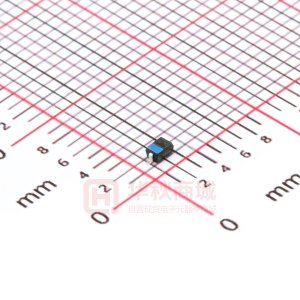
�Package SC79
BAR64...
Package Outline
0.2 0.8 ±0.1
10˚MAX.
M
A 0.13 -0.03
+0.05
2
1.6 ±0.1
0.55 ±0.04
Foot Print
1.35
0.35
Marking Layout (Example)
2005, June Date code
0.35
BAR63-02V Type code Cathode marking Laser marking
Standard Packing
Reel ø180 mm = 3.000 Pieces/Reel Reel ø180 mm = 8.000 Pieces/Reel (2 mm Pitch) Reel ø330 mm = 10.000 Pieces/Reel
Standard 4 Reel with 2 mm Pitch 2
0.2
1.33
1.96
Cathode marking
0.4 0.93
8
0.2 ±0.05
0.66
Cathode marking
1 0.3 ±0.05
Cathode marking
10˚MAX. 1.2 ±0.1
A
9
2007-12-11
�BAR64...
Date Code marking for discrete packages with one digit (SCD80, SC79, SC75 1) ) CES-Code
M onth 2 0 03
01 02 03 04 05 06 07 08 09 10 11 12 a b c d e f g h j k l n
2 0 04
p q r s t u v x y z 2 3
2005
A B C D E F G H J K L N
2006
P Q R S T U V X Y Z 4 5
2 0 07
a b c d e f g h j k l n
2008
p q r s t u v x y z 2 3
2009
A B C D E F G H J K L N
2010
P Q R S T U V X Y Z 4 5
2011
a b c d e f g h j k l n
2012
p q r s t u v x y z 2 3
2 0 13
A B C D E F G H J K L N
2014
P Q R S T U V X Y Z 4 5
1 ) New Marking Layout for SC75, implemented at October 2005.
.
10
2007-12-11
�Package SOD323
BAR64...
Package Outline
0.9 +0.2 -0.1
+0.2 1.25 -0.1
0 ±0.05 A
1.7 +0.2 -0.1
+0.05 0.3 -0.2
2 Cathode marking 1 0.3 +0.1 -0.05 0.25 M A
0.45 ±0.15 2.5 ±0.2
0.15 +0.1 -0.06
Foot Print
0.6
Marking Layout (Example)
0.8
1.7
0.8
BAR63-03W Type code Cathode marking Laser marking
Standard Packing
Reel ø180 mm = 3.000 Pieces/Reel Reel ø330 mm = 10.000 Pieces/Reel
4
0.2
2 2.9 8
Cathode marking
0.65 1.35
1
11
2007-12-11
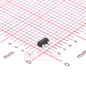
�Package SOT143
BAR64...
Package Outline
0.15 MIN.
2.9 ±0.1 1.9
4 3
B
1 ±0.1 0.1 MAX.
1.3 ±0.1
2.4 ±0.15
10˚ MAX.
1
2
10˚ MAX.
0.2 0.8 +0.1 -0.05 0.4 +0.1 -0.05 1.7 0.25 M B
0.08...0.1
A
5
0...8˚ 0.2 M A
Foot Print
0.8 1.2 0.8
0.9
1.2 0.8
0.8
Marking Layout (Example)
Manufacturer
RF s
Pin 1
56
Standard Packing
Reel ø180 mm = 3.000 Pieces/Reel Reel ø330 mm = 10.000 Pieces/Reel
0.9
1.1
2005, June Date code (YM)
BFP181 Type code
4
0.2
Pin 1
3.15
2.6 8
1.15
12
2007-12-11
�Package SOT23
BAR64...
Package Outline
0.15 MIN.
1 ±0.1 0.1 MAX.
1.3 ±0.1
2.9 ±0.1
3
B
2.4 ±0.15
10˚ MAX.
0.4 +0.1 -0.05
1)
1
2
10˚ MAX.
C 0.95 1.9
0.08...0.1
A
5
0...8˚
0.25 M B C
0.2
M
A
1) Lead width can be 0.6 max. in dambar area
Foot Print
0.8
0.9
0.8
1.2
Marking Layout (Example)
Manufacturer
EH s
Pin 1
0.9
1.3
2005, June Date code (YM)
BCW66 Type code
Standard Packing
Reel ø180 mm = 3.000 Pieces/Reel Reel ø330 mm = 10.000 Pieces/Reel
4 0.9
2.13 2.65
0.2
8
Pin 1
3.15
1.15
13
2007-12-11
�Package SOT323
BAR64...
Package Outline
2 ±0.2 0.3 +0.1 -0.05 3
1.25 ±0.1 2.1 ±0.1
0.9 ±0.1 3x 0.1
M
0.1 MAX. 0.1 A
1 0.65 0.65
2
0.1 MIN.
0.15 +0.1 -0.05 0.2
M
A
Foot Print
0.6
0.8
0.65 0.65
Marking Layout (Example)
Manufacturer
1.6
2005, June Date code (YM)
Pin 1
BCR108W Type code
Standard Packing
Reel ø180 mm = 3.000 Pieces/Reel Reel ø330 mm = 10.000 Pieces/Reel
4 0.2
Pin 1
2.15
2.3
8
1.1
14
2007-12-11
�Package TSLP-2-7
BAR64...
Package Outline
Top view
0.39 +0.01 -0.03 0.05 MAX.
0.65 ±0.05
Bottom view
0.6 ±0.05
2
2 1
1
Cathode marking
0.5 ±0.035 1)
1) Dimension applies to plated terminal
Foot Print
For board assembly information please refer to Infineon website "Packages"
0.35
0.45
0.3 0.925
1
0.275 0.275 0.375
0.6
Copper
Solder mask
0.35
Stencil apertures
Marking Layout (Example)
BAR90-02LRH Type code
Cathode marking Laser marking
Standard Packing
Reel ø180 mm = 15.000 Pieces/Reel Reel ø330 mm = 50.000 Pieces/Reel (optional)
4
1.16
0.5
Cathode marking
0.76
8
0.25 ±0.035 1)
1±0.05
15
2007-12-11
�BAR64...
Edition 2006-02-01 Published by Infineon Technologies AG 81726 München, Germany © Infineon Technologies AG 2007. All Rights Reserved.
Attention please! The information given in this dokument shall in no event be regarded as a guarantee of conditions or characteristics (“Beschaffenheitsgarantie”). With respect to any examples or hints given herein, any typical values stated herein and/or any information regarding the application of the device, Infineon Technologies hereby disclaims any and all warranties and liabilities of any kind, including without limitation warranties of non-infringement of intellectual property rights of any third party. Information For further information on technology, delivery terms and conditions and prices please contact your nearest Infineon Technologies Office (www.infineon.com ). Warnings Due to technical requirements components may contain dangerous substances. For information on the types in question please contact your nearest Infineon Technologies Office. Infineon Technologies Components may only be used in life-support devices or systems with the express written approval of Infineon Technologies, if a failure of such components can reasonably be expected to cause the failure of that life-support device or system, or to affect the safety or effectiveness of that device or system. Life support devices or systems are intended to be implanted in the human body, or to support and/or maintain and sustain and/or protect human life. If they fail, it is reasonable to assume that the health of the user or other persons may be endangered.
16
2007-12-11
�