BFP740
NPN Silicon Germanium RF Transistor • High gain ultra low noise RF transistor • Provides outstanding performance for a wide range of wireless applications up to 10 GHz and more • Ideal for CDMA and WLAN applications • Outstanding noise figure F = 0.5 dB at 1.8 GHz Outstanding noise figure F = 0.85 dB at 6 GHz • High maximum stable gain Gms = 27 dB at 1.8 GHz • Gold metallization for extra high reliability • 150 GHz fT-Silicon Germanium technology • Pb-free (RoHS compliant) package 1) • Qualified according AEC Q101
3 4 1
2
ESD (Electrostatic discharge) sensitive device, observe handling precaution!
Type BFP740
1Pb-containing
Marking R7s 1=B
Pin Configuration 2=E 3=C 4=E -
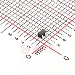
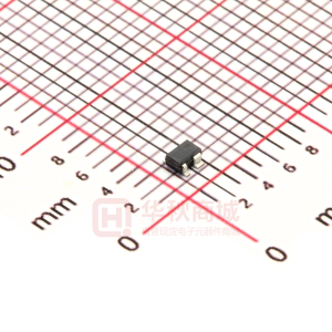
Package SOT343
package may be available upon special request
2009-12-04 1
�BFP740
Maximum Ratings Parameter Collector-emitter voltage TA > 0°C TA ≤ 0°C Collector-emitter voltage Collector-base voltage Emitter-base voltage Collector current Base current Total power dissipation1) TS ≤ 89°C Junction temperature Ambient temperature Storage temperature Thermal Resistance Parameter Junction - soldering point 2) Symbol RthJS Value ≤ 380 Unit K/W Tj TA T stg 150 -65 ... 150 -65 ... 150 °C VCES VCBO VEBO IC IB Ptot Symbol VCEO 4 3.5 13 13 1.2 30 3 160 mW mA Value Unit V
Electrical Characteristics at TA = 25°C, unless otherwise specified Parameter DC Characteristics Collector-emitter breakdown voltage IC = 1 mA, I B = 0 Collector-emitter cutoff current VCE = 13 V, VBE = 0 Collector-base cutoff current VCB = 5 V, IE = 0 Emitter-base cutoff current VEB = 0.5 V, IC = 0 DC current gain IC = 25 mA, VCE = 3 V, pulse measured
1T
Symbol min. V(BR)CEO ICES ICBO IEBO hFE 4 160
Values typ. 4.7 250 max. 30 100 3 400
Unit
V µA nA µA -
S is measured on the collector lead at the soldering point to the pcb 2For calculation of R thJA please refer to Application Note Thermal Resistance
2009-12-04 2
�BFP740
Electrical Characteristics at TA = 25°C, unless otherwise specified Symbol Values Unit Parameter min. typ. max. AC Characteristics (verified by random sampling) Transition frequency fT IC = 25 mA, VCE = 3 V, f = 2 GHz Collector-base capacitance VCB = 3 V, f = 1 MHz, V BE = 0 , emitter grounded Collector emitter capacitance VCE = 3 V, f = 1 MHz, V BE = 0 , base grounded Emitter-base capacitance VEB = 0.5 V, f = 1 MHz, VCB = 0 , collector grounded Noise figure IC = 8 mA, VCE = 3 V, f = 1.8 GHz, ZS = ZSopt IC = 8 mA, VCE = 3 V, f = 6 GHz, ZS = ZSopt Power gain, maximum stable1) IC = 25 mA, VCE = 3 V, ZS = ZSopt, ZL = ZLopt , f = 1.8 GHz Power gain, maximum available1) IC = 25 mA, VCE = 3 V, ZS = ZSopt, ZL = ZLopt, f = 6 GHz Transducer gain IC = 25 mA, VCE = 3 V, ZS = ZL = 50 Ω, f = 1.8 GHz f = 6 GHz Third order intercept point at output2) VCE = 3 V, I C = 25 mA, ZS =ZL=50 Ω, f = 1.8 GHz 1dB Compression point at output IC = 25 mA, VCE = 3 V, ZS =ZL=50 Ω, f = 1.8 GHz
1/2 ma = |S 21e / S12e| (k-(k²-1) ), Gms = |S21e / S12e | 2IP3 value depends on termination of all intermodulation frequency components. Termination used for this measurement is 50Ω from 0.1 MHz to 6 GHz
1G
-
42 0.08
0.14
GHz pF
Ccb
Cce
-
0.24
-
Ceb
-
0.44
-
F G ms 0.5 0.85 27 -
dB
dB
G ma
-
17
-
dB
|S21e|2 IP 3 P-1dB 24.5 13.5 25 11 -
dB
dBm
2009-12-04 3
�BFP740
Simulation Data For SPICE-model as well as for S-parameters including noise parameters refer to our internet website: www.infineon.com/rf.models. Please consult our website and download the latest version before actually starting your design. The simulation data have been generated and verified up to 12 GHz using typical devices. The BFP740 nonlinear SPICE-model reflects the typical DC- and RF-device performance with high accuracy.
2009-12-04 4
�BFP740
Total power dissipation Ptot = ƒ(TS) Permissible Pulse Load RthJS = ƒ(t p)
180
mW
10 3
140 120 100
K/W
RthJS
Ptot
10 2 80 60 40 20 0 0 10 1 -7 10
D = 0,5 0,2 0,1 0,05 0,02 0,01 0,005 0
15
30
45
60
75
90 105 120 °C
150
10
-6
10
-5
10
-4
10
-3
10
-2
s
10
0
TS
tp
Permissible Pulse Load Ptotmax/P totDC = ƒ(tp)
10 2
Collector-base capacitance Ccb = ƒ (V CB) f = 1 MHz
0.2
Ptotmax /PtotDC
0.18
0.16
0.14
Ccb [pF]
10
1
D=0 0.005 0.01 0.02 0.05 0.1 0.2 0.5
0.12
0.1
0.08
0.06
0.04
0.02
10
0
10
-7
10
-6
10
-5
10
-4
10
-3
10
-2
s
10
0
0 0 2 4 6 8 10 12
TP
VCB [V]
2009-12-04 5
�BFP740
Third order Intercept Point IP3 = ƒ (IC) (Output, ZS = ZL = 50 Ω ) VCE = parameter, f = 1.8 GHz
30
Transition frequency fT = ƒ(IC) f = 2 GHz VCE = parameter
50
27
4.00V 3.00V
45
2V to 4V
24 40
2.00V
21 35
18
30
IP3 [dBm]
15
fT [GHz]
1.00V
25
1.00V
20
12
9
15
0.75V
6 10
3
5
0.50V
0 0 5 10 15 20 25 30 35 0 0 5 10 15 20 25 30 35
I [mA]
C
I [mA]
C
Power gain Gma, Gms = ƒ (f) VCE = 3 V, I C = 25 mA
Power gain Gma, Gms = ƒ (IC) VCE = 3 V f = parameter
55
34
50
32
0.90GHz
30 45 28 40 26 35
1.80GHz 2.40GHz 3.00GHz
24
G [dB]
30
G [dB]
22
Gms
25
4.00GHz
20
G
20
5.00GHz
18
ma
6.00GHz |S21|
2
16
15 14 10
12
5 0 1 2 3 4 5 6
10 0 5 10 15 20 25 30 35
f [GHz]
IC [mA]
2009-12-04 6
�BFP740
Power gain Gma, Gms = ƒ (VCE) IC = 25 mA f = parameter
36
Noise figure F = ƒ(I C) VCE = 3V, f = parameter ZS = ZSopt
2
32
1.8
0.90GHz
28
1.6
1.80GHz 2.40GHz 3.00GHz 4.00GHz f = 6GHz f = 5GHz f = 3GHz f = 1.8GHz f = 0.9GHz
1.4
24
1.2
F [dB]
5
20
G [dB]
5.00GHz 6.00GHz
16
1
0.8
12
0.6
8
0.4
4
0.2
0 0 0.5 1 1.5 2 2.5 3 3.5 4 4.5
0 0 5 10
c
15
I [mA]
20
25
30
V
CE
[V]
Noise figure F = ƒ(IC ) VCE = 3V, f = 1.8 GHz
Noise figure F = ƒ(f) VCE = 3 V, ZS = ZSopt
2
1.4
1.8 1.2 1.6
Z = 50Ω
S
1.4
1
Z =Z
S
Sopt
1.2 0.8
F [dB] F [dB]
1
0.6 0.8
I = 25mA
C
0.6
0.4
I = 8mA C
0.4 0.2 0.2
0 0 5 10
c
0 15
I [mA]
20
25
30
0
1
2
3
f [GHz]
4
5
6
7
2009-12-04 7
�BFP740
Source impedance for min. noise figure vs. frequency VCE = 3 V, I C = 8 mA / 25 mA
1 1.5 0.5 0.4 0.3 0.2 0.1 0 −0.1 −0.2 −0.3 −0.4 −0.5 −1.5 −1 −2
I = 25mA
c
2
I = 8mA c
3 4 5
3GHz 0.2 0.4 4GHz 1
2.4GHz 1.8GHz 0.9GHz 2 4 5GHz 6GHz
10
6GHz
−10 −5 −4 −3
2009-12-04 8
�Package SOT343
BFP740
Package Outline
2 ±0.2 1.3 4 3 0.15 1 0.3 +0.1 -0.05 4x 0.1
M +0.1 0.6 -0.05
0.9 ±0.1 0.1 MAX. 0.1 A
1.25 ±0.1 2.1 ±0.1
2
0.1 MIN.
0.15 -0.05 0.2
M
+0.1
A
Foot Print
0.6
0.8
1.15 0.9
Marking Layout (Example)
Manufacturer
1.6
2005, June Date code (YM)
Pin 1
BGA420 Type code
Standard Packing
Reel ø180 mm = 3.000 Pieces/Reel Reel ø330 mm = 10.000 Pieces/Reel
4 0.2
Pin 1
2.15
2.3
8
1.1
2009-12-04 9
�BFP740
Edition 2009-11-16 Published by Infineon Technologies AG 81726 Munich, Germany
2009 Infineon Technologies AG All Rights Reserved.
Legal Disclaimer The information given in this document shall in no event be regarded as a guarantee of conditions or characteristics. With respect to any examples or hints given herein, any typical values stated herein and/or any information regarding the application of the device, Infineon Technologies hereby disclaims any and all warranties and liabilities of any kind, including without limitation, warranties of non-infringement of intellectual property rights of any third party.
Information For further information on technology, delivery terms and conditions and prices, please contact the nearest Infineon Technologies Office ().
Warnings Due to technical requirements, components may contain dangerous substances. For information on the types in question, please contact the nearest Infineon Technologies Office. Infineon Technologies components may be used in life-support devices or systems only with the express written approval of Infineon Technologies, if a failure of such components can reasonably be expected to cause the failure of that life-support device or system or to affect the safety or effectiveness of that device or system. Life support devices or systems are intended to be implanted in the human body or to support and/or maintain and sustain and/or protect human life. If they fail, it is reasonable to assume that the health of the user or other persons may be endangered.
2009-12-04 10
�