BSR92P
SIPMOS® Small-Signal-Transistor
Features • P-Channel • Enhancement mode / Logic level • Avalanche rated • Pb-free lead plating; RoHS compliant • Footprint compatible to SOT23
Product Summary V DS R DS(on),max ID -250 11 -0.14 V Ω A
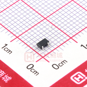
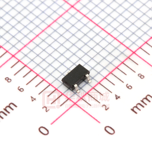
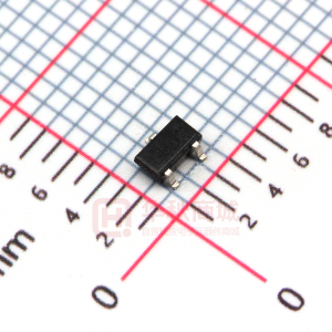
PG-SC59
Type BSR92P
Package PG-SC59
Tape and Reel Information L6327 = 3000 pcs. / reel
Marking LD
Lead free Yes
Packing Non dry
Maximum ratings, at T j=25 °C, unless otherwise specified Parameter Symbol Conditions Value steady state Continuous drain current ID T A=25 °C T A=70 °C Pulsed drain current Avalanche energy, single pulse Gate source voltage Power dissipation Operating and storage temperature ESD class Soldering temperature IEC climatic category; DIN IEC 68-1 I D,pulse E AS V GS P tot T j, T stg JESD22-A114 (HBM) T C=25 °C T A=25 °C I D=-0.14 A, R GS=25 Ω -0.14 -0.11 -0.56 24 ±20 0.5 -55 ... 150 1A (250V to 500V) 260 °C 55/150/56 mJ V W °C A Unit
Rev 1.02
page 1
2009-02-16
�BSR92P
Parameter Symbol Conditions min. Thermal characteristics Thermal resistance, junction - ambient R thJA minimal footprint, steady state Values typ. max. Unit
-
-
250
K/W
Electrical characteristics, at T j=25 °C, unless otherwise specified Static characteristics Drain-source breakdown voltage Gate threshold voltage V (BR)DSS V GS=0 V, I D=-250 µA V GS(th) V DS=V GS, I D=-130 µA V DS=-250 V, V GS=0 V, T j=25 °C V DS=-250 V, V GS=0 V, T j=150 °C Gate-source leakage current I GSS V GS=-20 V, V DS=0 V V GS=-2.8 V, I D=-0.025 A Drain-source on-state resistance R DS(on) V GS=-4.5 V, I D=0.13 A V GS=-10 V, I D=-0.14 A Transconductance g fs |V DS|>2|I D|R DS(on)max, I D=-0.11 A -250 -2 -1.5 -1 V
Zero gate voltage drain current
I DSS
-
-0.1
-1
µA
-
-10 -10 11
-100 -100 20 nA
-
9
13
Ω
-
8
11
0.1
0.3
-
S
Rev 1.02
page 2
2009-02-16
�BSR92P
Parameter Symbol Conditions min. Dynamic characteristics Input capacitance Output capacitance Reverse transfer capacitance Turn-on delay time Rise time Turn-off delay time Fall time Gate Charge Characteristics 2) Gate to source charge Gate to drain charge Gate charge total Gate plateau voltage Reverse Diode Diode continuous forward current Diode pulse current Diode forward voltage Reverse recovery time Reverse recovery charge IS I S,pulse V SD t rr Q rr V R=125 V, I F=|I S|, di F/dt =100 A/µs T C=25 °C V GS=0 V, I F=0.14 A, T j=25 °C -0.8 66 125 -0.14 -0.56 -1.2 V ns nC A Q gs Q gd Qg V plateau V DD=-200 V, I D=0.14 A, V GS=0 to -10 V -0.2 -1.2 -3.6 -2.7 -0.3 -1.8 -4.8 V nC C iss C oss C rss t d(on) tr t d(off) tf V DD=-125 V, V GS=-10 V, I D=-0.14 A, R G=6 Ω V GS=0 V, V DS=-25 V, f =1 MHz 82 12 5 6.4 6.3 75.0 71.0 109 16 8 9.0 9.0 112 163 ns pF Values typ. max. Unit
2)
See figure 16 for gate charge parameter definition
Rev 1.02
page 3
2009-02-16
�BSR92P
1 Power dissipation P tot=f(T C) 2 Drain current I D=f(T C); |V GS|≥10 V
0.6
0.15
0.5
0.4
0.1
P tot [W]
0.3
0.2
-I D [A]
0.05 0 0 40 80 120 160 0 40 80 120 160
0.1
0
T A [°C]
T A [°C]
3 Safe operating area I D=f(V DS); T C=25 °C; D =0 parameter: t p
100
limited by on-state resistance 1 ms 10 ms 100 µs
4 Max. transient thermal impedance Z thJC=f(t p) parameter: D =t p/T
103
0.5
102
0.2 0.1
10-1
100 ms
Z thJS [K/W]
-I D [A]
0.05
10
1
0.02 0.01 single pulse
DC
10-2 100
10-3 10
-1
10-1 10
0
10
1
10
2
10
3
10-5
10-4
10-3
10-2
10-1
100
101
102
-V DS [V]
t p [s]
Rev 1.02
page 4
2009-02-16
�BSR92P
5 Typ. output characteristics I D=f(V DS); T j=25 °C parameter: V GS
0.5
10 V 6V 4.5 V
6 Typ. drain-source on resistance R DS(on)=f(I D); T j=25 °C parameter: V GS
14
-2.5 V
0.4
3.5 V
-3 V
12
R DS(on) [Ω ]
0.3
3V
I D [A]
10
-3.5 V
0.2
-4.5 V -6 V 2.5 V
8
-10 V
0.1
2V
0 0 1 2 3 4 5
6 0 0.1 0.2 0.3 0.4
V DS [V]
-I D [A]
7 Typ. transfer characteristics I D=f(V GS); |V DS|>2|I D|R DS(on)max parameter: T j
0.5
25 °C
8 Typ. forward transconductance g fs=f(I D); T j=25 °C
0.4
0.4
150 °C
0.3
0.3
-I D [A]
g fs [S]
0.2 0.1 0 0 1 2 3 4
0.2
0.1
0 0.00 0.04 0.08 0.12 0.16
-V GS [V]
-I D [A]
Rev 1.02
page 5
2009-02-16
�BSR92P
9 Drain-source on-state resistance R DS(on)=f(T j); I D=-0.14 A; V GS=-10 V 10 Typ. gate threshold voltage V GS(th)=f(T j); V GS=V DS; I D=-130 µA
30
2.5
25
2
min
20
R DS(on) [mΩ]
15
98%
-V GS(th) [V]
1.5
typ
1
max
10
10V
0.5 5
0 -60 -40 -20 0 20 40 60 80 100 120 140 160
0 -60 -20 20 60 100 140
T j [°C]
T j [°C]
11 Typ. capacitances C =f(V DS); V GS=0 V; f =1 MHz
12 Forward characteristics of reverse diode I F=f(V SD) parameter: T j
1000
1
100
Ciss
0.1
25 °C 150 °C
C [pF]
Coss
10
Crss
I F [A]
0.01
150°C, 98%
25°C, 98%
1 0 20 40 60 80 100
0.001 0 0.4 0.8 1.2 1.6
-V DS [V]
-V SD [V]
Rev 1.02
page 6
2009-02-16
�BSR92P
13 Avalanche characteristics I AS=f(t AV); R GS=25 Ω parameter: T j(start)
100
14 Typ. gate charge V GS=f(Q gate); I D=-0.14 A pulsed parameter: V DD
10
8
50 V
25 °C
6
- VGS [V]
-I AV [A]
125 V
10-1
100 °C
4
125 °C
200 V
2
10-2 100 101 102 103
0 0 1 2 3
t AV [µs]
- Qgate [nC]
15 Drain-source breakdown voltage V BR(DSS)=f(T j); I D=-250 µA
16 Gate charge waveforms
300 290 280 270
V GS
Qg
-V BR(DSS) [V]
260 250 240 230 220 210 200 -60 -20 20 60 100 140
V g s(th)
Q g(th) Q gs
Q sw Q gd
Q g ate
T j [°C]
Rev 1.02
page 7
2009-02-16
�BSR92P
Package Outline SC-59: Outline
Footprint
Packaging Tape
Dimensions in mm Rev 1.02 page 8 2009-02-16
�BSR92P
Published by Infineon Technologies AG 81726 München, Germany © Infineon Technologies AG 2006. All Rights Reserved. Attention please! The information given in this data sheet shall in no event be regarded as a guarantee of conditions o characteristics (“Beschaffenheitsgarantie”). With respect to any examples or hints given herein, any typica values stated herein and/or any information regarding the application of the device, Infineon Technologies hereby disclaims any and all warranties and liabilities of any kind, including without limitation warranties o non-infringement of intellectual property rights of any third party Information For further information on technology, delivery terms and conditions and prices please contact your neares Infineon Technologies Office (www.infineon.com ). Warnings Due to technical requirements components may contain dangerous substances. For information on the types in question please contact your nearest Infineon Technologies Office. Infineon Technologies Components may only be used in life-support devices or systems with the express written approval of Infineon Technologies, if a failure of such components can reasonably be expected to cause the failure of that life-support device or system, or to affect the safety or effectiveness of that device or system. Life support devices or systems are intended to be implanted in the human body, or to support and/or maintain and sustain and/or protect human life. If they fail, it is reasonable to assume that the health of the user or other persons may be endangered.
Rev 1.02
page 9
2009-02-16
�
很抱歉,暂时无法提供与“BSR92P”相匹配的价格&库存,您可以联系我们找货
免费人工找货