BTS 441 T
Smart Highside Power Switch One Channel: 20mΩ
Product Summary
On-state Resistance Operating Voltage Nominal load current Current limitation RON Vbb(on) IL(ISO) IL(lim) 20mΩ 4.75 ... 41V 21A 65A
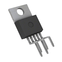
Package
TO-220-5-11 TO-263-5-2 TO-220-5-12
Standard
SMD
Straight
General Description
• • N channel vertical power FET with charge pump, ground referenced CMOS compatible input, monolithically integrated in Smart SIPMOS® technology. Providing embedded protective functions.
Application
• • • • µC compatible power switch for 5V, 12 V and 24 V DC applications All types of resistive, inductive and capacitve loads Most suitable for loads with high inrush currents, so as lamps Replaces electromechanical relays, fuses and discrete circuits
Basic Funktions
• • • • • Very low standby current Optimized static electromagnetic compatibility (EMC) µC and CMOS compatible Fast demagnetization of inductive loads Stable behaviour at undervoltage
Protection Functions
• • • • • • • • Short circuit protection Current limitation Overload protection Thermal shutdown Overvoltage protection (including load dump) with external GND-resistor Reverse battery protection with external GND-resistor Loss of ground and loss of Vbb protection Electrostatic discharge (ESD) protection
Vbb
IN
Logic with protection functions
OUT Load
PROFET GND
Infineon Technologies AG
1 of 11
2003-Oct-01
�BTS 441 T
Functional diagram
overvoltage protection internal voltage supply logic
gate control + charge pump
current limit
VBB
clamp for inductive load OUT
IN
ESD
temperature sensor LOAD
GND
PROFET
Pin Definitions and Functions Pin 1 2 3 4 5 Tab Symbol GND IN Vbb N.C. OUT Vbb Function Logic ground Input, activates the power switch in case of logical high signal Positive power supply voltage The tab is shorted to pin 3 Not connected Output to the load Positive power supply voltage The tab is shorted to pin 3
Pin configuration (top view)
Tab = VBB
1
2
(3)
4
5
GND IN
NC OUT
Infineon Technologies AG
2
2003-Oct-01
�BTS 441 T
Maximum Ratings at Tj = 25 °C unless otherwise specified Parameter Supply voltage (overvoltage protection see page 4) Supply voltage for full short circuit protection Tj Start=-40 ...+150°C Load dump protection1) VLoadDump = VA + Vs, VA = 13.5 V RI2)= 2 Ω, RL= 0,5 Ω, td= 200 ms, IN= low or high Load current (Short-circuit current, see page 5) Operating temperature range Storage temperature range Power dissipation (DC) ; TC≤25°C Maximal switchable inductance, single pulse Vbb = 12V, Tj,start = 150°C, TC = 150°C const. (see diagram, p.8) IL(ISO) = 21 A, RL= 0 Ω: E4)AS=0.7J: Electrostatic discharge capability (ESD) IN: (Human Body Model) Out to all other pins shorted:
acc. MIL-STD883D, method 3015.7 and ESD assn. std. S5.1-1993; R=1.5kΩ; C=100pF
Symbol Vbb Vbb VLoad dump3) IL Tj Tstg Ptot ZL VESD
Values 43 34 60 self-limited -40 ...+150 -55 ...+150 125 2.1 1.0 8.0 -10 ... +16 ±2.0 ≤1 ≤ 75 ≤ 33
Unit V V V A °C W mH kV
Input voltage (DC) Current through input pin (DC)
see internal circuit diagrams page 7
VIN IIN RthJC RthJA
V mA K/W
Thermal resistance
chip - case: junction - ambient (free air): SMD version, device on pcb5):
1) 2) 3) 4) 5)
Supply voltages higher than Vbb(AZ) require an external current limit for the GND pin, e.g. with a 150 Ω resistor in the GND connection. A resistor for the protection of the input is integrated. RI = internal resistance of the load dump test pulse generator VLoad dump is setup without the DUT connected to the generator per ISO 7637-1 and DIN 40839 EAS is the maximum inductive switch off energy Device on 50mm*50mm*1.5mm epoxy PCB FR4 with 6cm2 (one layer, 70µm thick) copper area for Vbb connection. PCB is vertical without blown air.
Infineon Technologies AG
3
2003-Oct-01
�BTS 441 T Electrical Characteristics
Parameter and Conditions
at Tj =-40...+150°C, Vbb = 12 V unless otherwise specified
Symbol
Values min typ max
Unit
Load Switching Capabilities and Characteristics On-state resistance (Vbb (pin3) to OUT (pin5)); IL = 2 A Vbb≥7V: Tj=25 °C: RON Tj=150 °C:
see diagram page 9
--
15 28 21 -90 110 ---
20 37 -2
200 250 1 1
mΩ
Nominal load current (pin 3 to 5) ‘ISO 10483-1, 6.7:VON=0.5V, TC=85°C Output current (pin 5) while GND disconnected or GND pulled up6), Vbb=30 V, VIN= 0,
see diagram page 7
IL(ISO) IL(GNDhigh)
17 -40 40 0.1 0.1
A mA
µs V/µs V/µs
Turn-on time IN Turn-off time IN RL = 12 Ω, Slew rate on 10 to 30% VOUT, RL = 12 Ω, Slew rate off 70 to 40% VOUT, RL = 12 Ω,
to 90% VOUT: ton to 10% VOUT: toff
dV /dton -dV/dtoff
Operating Parameters Operating voltage
Tj =-40°C Vbb(on) Tj =+25°C Tj =+105°C6) Tj =+150°C Overvoltage protection7) Tj =-40°C: Vbb(AZ) I bb = 40 mA Tj =+25...+150°C: Standby current (pin 3) 8) Tj=-40...+25°C: Ibb(off) Tj=+105°C6): VIN=0 see diagram page 9 Tj=+150°C: IL(off) Off-State output current (included in Ibb(off)) VIN=0 Operating current (Pin 1)9), VIN=5 V, IGND
4.75 4.75 4.75 5.0 41 43 ------
-----47 5 --1.5 2
41 43 43 43 -52 10 10 25 10 4
V
V µA µA mA
6) 7) 8) 9)
not subject to production test, specified by design see also VON(CL) in table of protection functions and circuit diagram page 7 Measured with load, typ. 40 µA without load. Add IIN, if VIN>5.5 V
Infineon Technologies AG
4
2003-Oct-01
�BTS 441 T
Parameter and Conditions
at Tj =-40...+150°C, Vbb = 12 V unless otherwise specified
Symbol
Values min typ max
Unit
Protection Functions10) Current limit (pin 3 to 5)
(see timing diagrams, page 9)
IL(lim) Tj =-40°C: Tj =25°C: =+150°C: Tj IL(SCr) Tj,start =25°C: Toff(SC) --40 --41 43 150 ----65 -55 14 -47 -10 -540 85 -----52 --32 -A A ms V °C K V mV
Repetitive short circuit current limit Tj = Tjt (see timing diagrams, page 10) Thermal shutdown time11)12)
(see timing diagram on page 10)
;Tj =-40°C: Tj=25..150°C: VON(CL) Thermal overload trip temperature Tjt Thermal hysteresis ∆Tjt Reverse battery (pin 3 to 1) 13) -Vbb Reverse battery voltage drop (VOUT > Vbb) -VON(rev) IL = -2A Tj =+150°C: at VOUT = Vbb - VON(CL), IL= 40 mA
Output clamp (inductive load switch off)
10)
Integrated protection functions are designed to prevent IC destruction under fault conditions described in the data sheet. Fault conditions are considered as "outside" normal operating range. Protection functions are not designed for continuous repetitive operation. 11) not subject to production test, specified by design 12) Device on 50mm*50mm*1.5mm epoxy PCB FR4 with 6cm2 (one layer, 70µm thick) copper area for V bb connection. PCB is vertical without blown air. 13) Requires 150 Ω resistor in GND connection. The reverse load current through the intrinsic drain-source diode has to be limited by the connected load. Note that the power dissipation is higher compared to normal operating conditions due to the voltage drop across the intrinsic drain-source diode. The temperature protection is not active during reverse current operation! Input and Status currents have to be limited (see max. ratings page 1 and circuit page 7).
Infineon Technologies AG
5
2003-Oct-01
�BTS 441 T
Parameter and Conditions
at Tj =-40...+150°C, Vbb = 12 V unless otherwise specified
Symbol
Values min typ max
Unit
Input14) Input resistance Input turn-on threshold voltage Input turn-off threshold voltage Input threshold hysteresis Off state input current (pin 2) On state input current (pin 2)
see circuit page 7
RI VIN(T+) VIN(T-) ∆ VIN(T) VIN = 0.4 V: IIN(off) VIN = 5 V: IIN(on)
2.5 1.2 0.8 -1 4.5
3.8 --0.3 -12
6.5 2.2 --15 24
kΩ V V V µA µA
14)
If a ground resistor RGND is used, add the voltage drop across this resistor.
Infineon Technologies AG
6
2003-Oct-01
�BTS 441 T
Terms
V Ibb bb I IN IN 2 V IN PROFET OUT 5
V Z1
Overvolt. and reverse batt. protection
+ Vbb V
Leadframe, 3 Vbb IL VON
R IN
IN
Z2
RI Logic
OUT
GND 1 R GND
PROFET
GND
IGND
VOUT
R GND
Signal GND
R Load
Load GND
Input circuit (ESD protection)
R IN I
VZ1 = 6.1 V typ., VZ2 = 47 V typ., RGND = 150 Ω, RI= 3.5 kΩ typ. In case of reverse battery the load current has to be limited by the load. Temperature protection is not active
ESD-ZD I GND
GND disconnect
I I
The use of ESD zener diodes as voltage clamp at DC conditions is not recommended.
IN
Vbb PROFET OUT
Inductive and overvoltage output clamp
+ V bb V Z
GND V bb V IN V GND
V
ON
Any kind of load. In case of Input=high is VOUT ≈ VIN - VIN(T+) .
OUT GND
PROFET
GND disconnect with GND pull up
VON clamped to 47 V typ.
Vbb IN PROFET OUT
GND
V
V bb
IN
V
GND
Any kind of load. If VGND > VIN - VIN(T+) device stays off
Infineon Technologies AG
7
2003-Oct-01
�BTS 441 T
Vbb disconnect with charged inductive load Inductive load switch-off energy dissipation
E bb E AS
Vbb high IN PROFET OUT
Vbb IN PROFET GND OUT
ELoad
GND
=
ZL
V
bb
{
R L
L
EL
ER
For inductive load currents up to the limits defined by ZL (max. ratings and diagram on page 8) each switch is protected against loss of Vbb. Consider at your PCB layout that in the case of Vbb disconnection with energized inductive load all the load current flows through the GND connection.
Energy stored in load inductance: EL = 1/2·L·I L While demagnetizing load inductance, the energy dissipated in PROFET is EAS= Ebb + EL - ER= VON(CL)·iL(t) dt, with an approximate solution for RL > 0 Ω: EAS= IL· L (V + |VOUT(CL)|) 2·RL bb IL·RL
2
ln (1+ |V
OUT(CL)|
)
Maximum allowable load inductance for a single switch off
L = f (IL ); Tj,start = 150°C, Vbb = 12 V, RL = 0 Ω L [mH]
1000
100
10
1
0.1 0 5 10 15 20 25 30 35
IL [A]
Infineon Technologies AG
Page 8
2003-Oct-01
�BTS 441 T
Typ. on-state resistance
RON = f (Vbb,Tj ); IL = 2 A, IN = high RON [mΩ]
40 35 30 25 20 15 10 5 3 5 7 9 30 40
Vbb [V]
Tj = 150°C
25°C -40°C
Typ. standby current
Ibb(off) = f (Tj ); Vbb = 9...34 V, IN1,2 = low Ibb(off) [µA]
20
15
10
5
0 -50
0
50
100
150
200
Tj [°C]
Infineon Technologies AG
Page 9
2003-Oct-01
�BTS 441 T
Timing diagrams
Figure 1a: Vbb turn on:
IN
Figure 2b: Switching a lamp,
IN
V
OUT
V bb
I
L
t
V
OUT
Figure 3a: Short circuit shut down by overtemperature, reset by cooling
proper turn on under all conditions
IN
other channel: normal operation
Figure 2a: Switching a resistive load, turn-on/off time and slew rate definition:
I
L
I
IN
L(lim) I L(SCr)
VOUT
90% t on dV/dton 10% t dV/dtoff
t
off(SC)
t
Heating up may require several milliseconds, depending on external conditions
off
Figure 4a: Overtemperature: Reset if Tj