Smart High-Side Power Switch BTS5210L
6PDUW +LJK�6LGH 3RZHU 6ZLWFK 7ZR &KDQQHOV� � [ ���P٠6WDWXV )HHGEDFN
Product Summary
2SHUDWLQJ 9ROWDJH 9EE $FWLYH FKDQQHOV 2Q�VWDWH 5HVLVWDQFH 521 1RPLQDO ORDG FXUUHQW ,/�120� &XUUHQW OLPLWDWLRQ ,/�6&U� ��������9 RQH WZR SDUDOOHO ���P٠��P٠���$ ���$ ���$ ���$
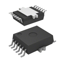
Package
P-DSO-12
PG-DSO-12-9
*HQHUDO 'HVFULSWLRQ
• •
1 FKDQQHO YHUWLFDO SRZHU 026)(7 ZLWK FKDUJH SXPS� JURXQG UHIHUHQFHG &026 FRPSDWLEOH LQSXW DQG GLDJQRVWLF IHHGEDFN� PRQROLWKLFDOO\ LQWHJUDWHG LQ 6PDUW 6,3026 WHFKQRORJ\� 3URYLGLQJ HPEHGGHG SURWHFWLYH IXQFWLRQV
$SSOLFDWLRQV
• • • •
& FRPSDWLEOH KLJK�VLGH SRZHU VZLWFK ZLWK GLDJQRVWLF IHHGEDFN IRU ��9 DQG ��9 JURXQGHG ORDGV $OO W\SHV RI UHVLVWLYH� LQGXFWLYH DQG FDSDFLWYH ORDGV 0RVW VXLWDEOH IRU ORDGV ZLWK KLJK LQUXVK FXUUHQWV� VR DV ODPSV 5HSODFHV HOHFWURPHFKDQLFDO UHOD\V� IXVHV DQG GLVFUHWH FLUFXLWV
%DVLF )XQFWLRQV
• • • • • • •
9HU\ ORZ VWDQGE\ FXUUHQW &026 FRPSDWLEOH LQSXW ,PSURYHG HOHFWURPDJQHWLF FRPSDWLELOLW\ �(0&� )DVW GHPDJQHWL]DWLRQ RI LQGXFWLYH ORDGV 6WDEOH EHKDYLRXU DW XQGHUYROWDJH :LGH RSHUDWLQJ YROWDJH UDQJH /RJLF JURXQG LQGHSHQGHQW IURP ORDG JURXQG
3URWHFWLRQ )XQFWLRQV
• • • • • • • •
Block Diagram
9EE
,1� 67� ,1� 67�
6KRUW FLUFXLW SURWHFWLRQ 2YHUORDG SURWHFWLRQ &XUUHQW OLPLWDWLRQ 7KHUPDO VKXWGRZQ 2YHUYROWDJH SURWHFWLRQ �LQFOXGLQJ ORDG GXPS� ZLWK H[WHUQDO UHVLVWRU 5HYHUVH EDWWHU\ SURWHFWLRQ ZLWK H[WHUQDO UHVLVWRU /RVV RI JURXQG DQG ORVV RI 9EE SURWHFWLRQ (OHFWURVWDWLF GLVFKDUJH SURWHFWLRQ �(6'�
/RJLF &KDQQHO � &KDQQHO �
/RDG � /RDG �
'LDJQRVWLF )XQFWLRQ
• • •
'LDJQRVWLF IHHGEDFN ZLWK RSHQ GUDLQ RXWSXW 2SHQ ORDG GHWHFWLRQ LQ 2))�VWDWH )HHGEDFN RI WKHUPDO VKXWGRZQ LQ 21�VWDWH
*1'
• AEC qualified • Green product (RoHS compliant)
Data Sheet 1 V1.1, 2007-05-29
�Smart High-Side Power Switch BTS5210L
)XQFWLRQDO GLDJUDP
*1'
LQWHUQDO YROWDJH VXSSO\
,1� 67�
ORJLF
JDWH FRQWURO � FKDUJH SXPS WHPSHUDWXUH VHQVRU 2SHQ ORDG GHWHFWLRQ FKDQQHO �
FXUUHQW OLPLW
9%%
FODPS IRU LQGXFWLYH ORDG
287�
(6'
UHYHUVH EDWWHU\ SURWHFWLRQ
,1� 67�
control and protection circuit equivalent to channel 1
287�
Data Sheet
2
V1.1, 2007-05-29
�Smart High-Side Power Switch BTS5210L
Pin Definitions and Functions
Pin 1 2 4 3 5 6,12, heat slug 7,9,11 8 10 Symbol Function GND Ground of chip IN1 Input 1,2 activates channel 1,2 in case of logic high signal IN2 ST1 Diagnostic feedback 1 & 2 of channel 1,2 open drain, low on failure ST2 Vbb Positive power supply voltage. Design the wiring for the simultaneous max. short circuit currents from channel 1 to 2 and also for low thermal resistance NC Not Connected OUT2 Output 1,2 protected high-side power output of channel 1 and 2. Design the wiring for the OUT1 max. short circuit current
Pin configuration
(top view)
GND IN1 ST1 IN2 ST2 Vbb
1• 2 3 4 5 6
Vbb*
12 11 10 9 8 7
Vbb NC OUT1 NC OUT2 NC
* heat slug
Data Sheet
3
V1.1, 2007-05-29
�Smart High-Side Power Switch BTS5210L
Parameter Supply voltage (overvoltage protection see page 6) Supply voltage for full short circuit protection Tj,start = -40 ...+150°C Load current (Short-circuit current, see page 6) Load dump protection1) VLoadDump = VA + Vs, VA = 13.5 V RI2) = 2 Ω, td = 400 ms; IN = low or high, each channel loaded with RL = 13.5 Ω, Operating temperature range Storage temperature range Power dissipation (DC)4) Ta = 25°C: (all channels active) Ta = 85°C: Maximal switchable inductance, single pulse Vbb = 12V, Tj,start = 150°C4), see diagrams on page 10 IL = 2.9 A, EAS = 84 mJ, 0 Ω one channel: IL = 5.7 A, EAS = 168 mJ, 0 Ω two parallel channels: Electrostatic discharge capability (ESD) IN: (Human Body Model) ST: out to all other pins shorted:
acc. MIL-STD883D, method 3015.7 and ESD assn. std. S5.1-1993 R=1.5kΩ; C=100pF
Symbol
Values 43 36 self-limited 60 -40 ...+150 -55 ...+150 3,05 1,59
Unit V V A V °C W
Vbb Vbb IL VLoad dump3) Tj Tstg Ptot
ZL
14 7.6 1.0 4.0 8.0 -10 ... +16 ±0.3 ±5.0 ±5.0
mH kV
VESD
Input voltage (DC) see internal circuit diagram page 9 Current through input pin (DC) Pulsed current through input pin5) Current through status pin (DC)
VIN IIN IINp IST
V mA
1) 2) 3) 4) 5)
Supply voltages higher than Vbb(AZ) require an external current limit for the GND and status pins (a 150Ω resistor for the GND connection is recommended. RI = internal resistance of the load dump test pulse generator VLoad dump is setup without the DUT connected to the generator per ISO 7637-1 and DIN 40839 Device on 50mm*50mm*1.5mm epoxy PCB FR4 with 6cm2 (one layer, 70µm thick) copper area for Vbb connection. PCB is vertical without blown air. See page 14 only for testing
4 V1.1, 2007-05-29
Data Sheet
�Smart High-Side Power Switch BTS5210L
Parameter and Conditions Thermal resistance junction - Case6) junction – ambient6) @ 6 cm2 cooling area
Symbol
Values min typ max ------45 40 5 ----
Unit
each channel: RthjC Rthja one channel active: all channels active:
K/W
Electrical Characteristics
Parameter and Conditions, each of the four channels
at Tj = -40...+150°C, Vbb = 12 V unless otherwise specified
Symbol
Values min typ max
Unit
Load Switching Capabilities and Characteristics On-state resistance (Vbb to OUT); IL = 2 A each channel, Tj = 25°C: RON Tj = 150°C: two parallel channels, Tj = 25°C:
see diagram, page 11
---1.8 3.4 --
110 210 55 2.4 3.9 --
140 280 70 --
mΩ
Nominal load current
one channel active: IL(NOM) two parallel channels active:
A
Device on PCB6), Ta = 85°C, Tj ≤ 150°C
Output current while GND disconnected or pulled up7); IL(GNDhigh)
Vbb = 32 V, VIN = 0, see diagram page 9 Turn-on time8)
2
mA µs
Turn-off time RL = 12 Ω Slew rate on 8) Slew rate off 8)
IN IN
to 90% VOUT: ton to 10% VOUT: toff
--0.2 0.2
100 100 ---
250 270 1.0 1.1
10 to 30% VOUT, RL = 12 Ω: dV/dton 70 to 40% VOUT, RL = 12 Ω: -dV/dtoff
V/µs V/µs
6) 7) 8)
Device on 50mm*50mm*1.5mm epoxy PCB FR4 with 6cm2 (one layer, 70µm thick) copper area for Vbb connection. PCB is vertical without blown air. See page 14 not subject to production test, specified by design See timing diagram on page 12.
5 V1.1, 2007-05-29
Data Sheet
�Smart High-Side Power Switch BTS5210L
Parameter and Conditions, each of the four channels
at Tj = -40...+150°C, Vbb = 12 V unless otherwise specified
Symbol
Values min typ max 5.5 --41 -------47 4.5 --1 40 4.5 4.510) 52 8 12 810) 5
Unit
Operating Parameters Operating voltage Undervoltage switch off9) Overvoltage protection11) I bb = 40 mA Standby current12) VIN = 0; see diagram page 11
Vbb(on) Tj =-40°C...25°C: Vbb(u so) Tj =125°C: Vbb(AZ)
V V V µA µA
Tj =-40°C...25°C: Ibb(off) Tj =150°C: Tj =125°C: Off-State output current (included in Ibb(off)) IL(off) VIN = 0; each channel Operating current 13), VIN = 5V, one channel on: IGND all channels on:
Protection Functions14) Current limit, Vout = 0V, (see timing diagrams, page 12) Tj =-40°C: IL(lim) Tj =25°C: =+150°C: Tj Repetitive short circuit current limit, Tj = Tjt each channel IL(SCr) two channels
(see timing diagrams, page 12)
---
0.5 1.0
0.9 1.7
mA
--5 ---41 150 --
-9 -6.5 6.5 2 47 -10
14 -----52 ---
A
A ms V
Initial short circuit shutdown time
Vout = 0V
Tj,start =25°C: toff(SC) VON(CL) Tjt ∆Tjt
(see timing diagrams on page 12)
Output clamp (inductive load switch off)15)
at VON(CL) = Vbb - VOUT, IL= 40 mA
Thermal overload trip temperature Thermal hysteresis
°C K
9) 10 11)
12) 13) 14)
15)
is the voltage, where the device doesn´t change it´s switching condition for 15ms after the supply voltage falling below the lower limit of Vbb(on) not subject to production test, specified by design Supply voltages higher than Vbb(AZ) require an external current limit for the GND and status pins (a 150Ω resistor for the GND connection is recommended). See also VON(CL) in table of protection functions and circuit diagram on page 9. Measured with load; for the whole device; all channels off Add IST, if IST > 0 Integrated protection functions are designed to prevent IC destruction under fault conditions described in the data sheet. Fault conditions are considered as "outside" normal operating range. Protection functions are not designed for continuous repetitive operation. If channels are connected in parallel, output clamp is usually accomplished by the channel with the lowest VON(CL)
Data Sheet
6
V1.1, 2007-05-29
�Smart High-Side Power Switch BTS5210L
Parameter and Conditions, each of the four channels
at Tj = -40...+150°C, Vbb = 12 V unless otherwise specified
Symbol
Values min typ max
Unit
Reverse Battery Reverse battery voltage 16) Drain-source diode voltage (Vout > Vbb) IL = - 2.0 A, Tj = +150°C Diagnostic Characteristics Open load detection voltage
-Vbb -VON
---
-600
32 --
V mV
V OUT(OL)
1
1.7
2.8
4.0
V
Input and Status Feedback17) Input resistance
(see circuit page 9)
RI VIN(T+) VIN(T-) ∆ VIN(T) td(STon) td(STon) td(SToff) td(SToff) IIN(off) IIN(on) VST(high) VST(low)
2.5 -1.0 --30 --5 10 5.4 --
4.0 --0.2 10 ----35 ---
6.0 2.5 --20 -500 20 20 60 -0.6
kΩ V V V s s s s µA µA V
Input turn-on threshold voltage Input turn-off threshold voltage Input threshold hysteresis Status change after positive input slope18) with open load Status change after positive input slope18) with overload Status change after negative input slope with open load Status change after negative input slope18) with overtemperature Off state input current VIN = 0.4 V: On state input current VIN = 5 V: Status output (open drain) Zener limit voltage IST = +1.6 mA: ST low voltage IST = +1.6 mA:
Requires a 150 Ω resistor in GND connection. The reverse load current through the intrinsic drain-source diode has to be limited by the connected load. Power dissipation is higher compared to normal operating conditions due to the voltage drop across the drain-source diode. The temperature protection is not active during reverse current operation! Input and Status currents have to be limited (see max. ratings page 4 and circuit page 9). 17) If ground resistors R GND are used, add the voltage drop across these resistors. 18) not subject to protection test, specified by design Data Sheet 7 V1.1, 2007-05-29
16)
�Smart High-Side Power Switch BTS5210L
Truth Table
( each channel )
IN Normal operation Open load Overtemperature L H L H L H OUT L H Z H L L ST H H L19) H H L
L = "Low" Level H = "High" Level
X = don't care Z = high impedance, potential depends on external circuit Status signal valid after the time delay shown in the timing diagrams
Parallel switching of channel 1 and 2 is easily possible by connecting the inputs and outputs in parallel (see truth table). If switching channel 1 to 2 in parallel, the status outputs ST1 and ST2 have to be configured as a 'Wired OR' function with a single pull-up resistor.
Terms
,EE 9 EE , ,1� , ,1� 9,1� 9 ,1� 9 , 67� , 67� 67� 9 67� 5 � � � � ���� ,1� ,1� 67� 67� *1' � , *1' *1' 9 287� /HDGIUDPH �� 9 21� 9 21� , /� , /� 9
9EE 287� 352)(7 287�
�
287�
Leadframe (Vbb) is connected to pin 6,12 External RGND optional; single resistor RGND = 150 Ω for reverse battery protection up to the max. operating voltage.
19)
L, if potential at the Output exceeds the OpenLoad detection voltage
Data Sheet
8
V1.1, 2007-05-29
�Smart High-Side Power Switch BTS5210L
Input circuit (ESD protection), IN1 or IN2
,1 5 ,
Overvolt. and reverse batt. protection
� �9 � 9EE 9
5 67
,1
5, /RJLF
=�
(6'�=' , *1'
,
,
5 67 67
9 =�
287
The use of ESD zener diodes as voltage clamp at DC conditions is not recommended.
*1'
5 *1'
6LJQDO *1'
5 /RDG
/RDG *1'
Status output, ST1 or ST2
��9
5 67�21�
67
VZ1 = 6.1 V typ., VZ2 = 47 V typ., RGND = 150 Ω, RST= 15 kΩ, RI= 3.5 kΩ typ. In case of reverse battery the load current has to be limited by the load. Temperature protection is not active
*1'
(6'� ='
Open-load detection, OUT1 or OUT2
OFF-state diagnostic condition: Open Load, if VOUT > 3 V typ.; IN low
9
ESD-Zener diode: 6.1 V typ., max 0.3 mA; RST(ON) < 375 Ω at 1.6 mA. The use of ESD zener diodes as voltage clamp at DC conditions is not recommended.
EE
Inductive and overvoltage output clamp,
OUT1 or OUT2
�9EE 9= 9
5 (;7
2))
9 287
/RJLF XQLW
21
2SHQ ORDG GHWHFWLRQ
287
6LJQDO *1'
GND disconnect
3RZHU *1'
VON clamped to VON(CL) = 47 V typ.
,1
9EE 352)(7 287
67 *1' 9 EE 9 ,1 9 67 9 *1'
Any kind of load. In case of IN = high is VOUT ≈ VIN - VIN(T+). Due to VGND > 0, no VST = low signal available.
Data Sheet
9
V1.1, 2007-05-29
�Smart High-Side Power Switch BTS5210L
GND disconnect with GND pull up
Inductive load switch-off energy dissipation
( EE ( $6
,1
9EE 352)(7 287
67 *1'
,1
9EE 352)(7 287
(/RD
9
EE
9
,1 67
9
67
9 *1'
*1'
=/
^
5 /
/
(/
(5
Any kind of load. If VGND > VIN - VIN(T+) device stays off Due to VGND > 0, no VST = low signal available.
Energy stored in load inductance:
Vbb disconnect with energized inductive load
EL = 1/2·L·I L
While demagnetizing load inductance, the energy dissipated in PROFET is
2
KLJK
,1
9EE 352)(7 287
EAS= Ebb + EL - ER= VON(CL)·iL(t) dt,
with an approximate solution for RL > 0 Ω: IL· L (V + |VOUT(CL)|) 2·RL bb IL·RL
67 *1'
EAS=
OQ (1+ |V
OUT(CL)|
)
9
Maximum allowable load inductance for a single switch off (one channel)4)
EE
/
I �,/ �� Tj,start = 150°C, Vbb = 12 V, RL = 0 Ω
����
For inductive load currents up to the limits defined by ZL (max. ratings and diagram on page 10) each switch is protected against loss of Vbb. Consider at your PCB layout that in the case of Vbb disconnection with energized inductive load all the load current flows through the GND connection.
ZL [mH]
���
��
� � � � � � �
IL [A]
Data Sheet 10 V1.1, 2007-05-29
�Smart High-Side Power Switch BTS5210L
Typ. on-state resistance
521 I �9EE�7M �; IL = 2 A, IN = high RON [mOhm]
���
7M
���&
��� ��& ���& ��
���
� � � � �� �� ��
Vbb [V]
Typ. standby current
,EE�RII�
�� �� �� �� �� �� �� �� � � ��� � �� ��� ��� ���
I �7M �; Vbb = 9...34 V, IN1,2 = low
Ibb(off) [µA]
Tj [°C]
Data Sheet
11
V1.1, 2007-05-29
�Smart High-Side Power Switch BTS5210L
Timing diagrams
All channels are symmetric and consequently the diagrams are valid for channel 1 to channel 4
Figure 1a: Vbb turn on: ,1� Figure 2b: Switching a lamp:
,1
,1� 9 EE 9
67
287�
9
287
9
287�
67� RSHQ GUDLQ
,
/
67� RSHQ GUDLQ W
W
Figure 2a: Switching a resistive load, turn-on/off time and slew rate definition:
Figure 3a: Turn on into short circuit: shut down by overtemperature, restart by cooling
,1� R WKHU FKDQQHO� QRUP DO RSHUDWLRQ
,1
9287
,
��
/�
W on G9�GWRQ W
G9�GWRII
,
/�OLP� , /�6&U�
��
off
W RII�6&�
,/
67
W
W
Data Sheet 12
Heating up of the chip may require several milliseconds, depending on external conditions
V1.1, 2007-05-29
�Smart High-Side Power Switch BTS5210L
Figure 3b: Turn on into short circuit: shut down by overtemperature, restart by cooling (two parallel switched channels 1 and 2)
,1���
Figure 5a: Open load: detection in OFF-state, turn on/off to open load Open load of channel 1; other channels normal operation
,1�
,
/�
�,
/�
9287�
�[,/�OLP�
,
, /�
/�6&U�
W 67���
67
RII�6&�
��V ���V
W
ST1 and ST2 have to be configured as a 'Wired OR' function ST1/2 with a single pull-up resistor.
Figure 4a: Overtemperature: Reset if Tj